
 Open Access Article
 This Open Access Article is licensed under a Creative Commons Attribution-Non Commercial 3.0 Unported Licence
Preparation and evaluation of the microwave absorption properties of template-free graphene foam-supported Ni nanoparticles†
Liangliang Xiong,
Mei Yu *,
Jianhua Liu,
Songmei Li and
Bing Xue
*,
Jianhua Liu,
Songmei Li and
Bing Xue
School of Materials Science and Engineering, Beihang University, Beijing 100191, China. E-mail: yumei@buaa.edu.cn; Fax: +86 10 82317103; Tel: +86 10 82317103
First published on 6th March 2017
Abstract
A template-free graphene foam-supported Ni nanoparticle (GFN) composite was prepared by a hydrothermal method, followed by a calcination process. Phase, composition and morphology of the composites were characterized by XRD, Raman spectroscopy, FTIR, XPS, FESEM, and TEM. GFN exhibited a well-defined and interconnected three-dimensional (3D) network structure without template, and Ni nanoparticles were uniformly dispersed on the graphene nanosheets and attached via C–Ni covalent bonds. The microwave absorption (MA) properties of the samples were also investigated with a vector network analyzer. Based on the 3D structure of graphene foam, due to interfacial effects (graphene/Ni/wax) and the synergistic effect between graphene and Ni nanoparticles, GFN showed the most remarkable MA properties, compared with the graphene foam-supported NiO nanoparticles composite (GFNO), pure graphene foam (GF) and pure Ni nanoparticles. When the thickness of the GFN/wax sample was 3.4 mm and the content of GFN in the sample was only 1 wt%, the maximum reflection loss of GFN could reach −49 dB at 11.5 GHz. This high reflection loss was a result of the multiple reflections and attenuations of electromagnetic waves within the 3D structure of the graphene foam, the interfacial polarization and the better impedance matching characteristics of GFN. Hence, a template-free graphene foam-supported Ni nanoparticle composite with strong absorption and lightweight properties showed a promising future in microwave absorption applications.
Introduction
Recently, microwave absorption (MA) materials have received increasing attention since the electromagnetic (EM) interference problem is becoming more serious due to the widespread use of electronic and telecommunication devices in industry, commerce and military affairs.1–3 As is well known, high-performance MA materials should possess a broad absorption bandwidth, strong absorption, low density and low thickness. Graphene, a two-dimensional carbon nanostructured material, has been used for MA materials owing to its stable structure, lightweight properties, high specific surface area and excellent electrical conductivity.4,5 Particularly, reduced graphene oxide (rGO) synthesized by chemical reduction of graphene oxide (GO) is a potential MA material because rGO not only promotes the transition of the continuous state to the Fermi energy level, but also introduces polarization relaxation due to its defects and functional groups.6,7However, pristine graphene is non-magnetic and the maximum reflection loss (RL) is only −6.9 dB due to its high dielectric constant.8,9 To balance the electromagnetic parameters and improve the impedance matching characteristics of pure graphene, a variety of materials were used to decorate graphene, such as Fe,10 Co,11 Ni,6 Fe3O4,12–14 carbonyl iron,15,16 CuS,17,18 and ferrite.19–21 He et al.13 synthesized laminated magnetic graphene (graphene@cubic Fe3O4 and graphene@spherical Fe3O4); the maximum RL was 26.4 dB at 5.3 GHz with a weight ratio of about 40% and a thickness of 4.0 mm, and the absorption bandwidth for the RL below −10 dB (90% absorption) was 2 GHz. Zhu et al.6 produced reduced graphene oxide–nickel (rGO–Ni) composites by a microwave-assisted method. The RL of the composites reached −42 dB at 17.6 GHz with a thickness of 2 mm, which was mainly due to the synergistic effect of the dielectric loss, magnetic loss and the dramatic electron polarization caused by the formation of a large conductive network. In summary, these studies have proved that modifying graphene with magnetic materials is an efficient method to enhance the MA properties of graphene.
Compared with the MA properties of graphene sheets, the three-dimensional (3D) graphene foam (GF) shows a broader absorption band as well as a lower RL due to the individual 3D interconnected graphene network, thin cell wall and superior electrical conductivity. Huang et al.22 fabricated a 3D bonded graphene foam by a solvothermal method and investigated the MA performance of the cubic graphene sponge in the frequency ranges of 2–18, 26.5–40, and 75–110 GHz. The results showed that the absorption bandwidth for the RL below −10 dB was 52.5 GHz (the total bandwidth was 64.5 GHz), and the maximum RL was about −38 dB in the range of 2–18 GHz. The 3D structure of graphene foam greatly reduces impedance gap, attenuates back-reflections and scattering among the cell walls, and thus enhances the absorption of microwave energy.
Similar to the improved MA properties of graphene sheets, the GF decorated with magnetic materials could have better impedance matching characteristics and enhanced MA properties with respect to pristine GF. In addition, as a typical soft magnetic material, Ni could be used as an absorbent in the high frequency range (over gigahertz), ascribed to the higher Snoek's limit.23 To avoid the eddy current effects induced by alternating electromagnetic waves and to decrease the permeability of nickel, the size of Ni particles should be less than the skin depth. Therefore, we fabricated the template-free graphene foam-supported Ni nanoparticle (GFN) composite by a hydrothermal method, followed by a calcination process. The electromagnetic data showed that GFN has the best microwave absorption properties compared with the graphene foam-supported NiO nanoparticles composite (GFNO), GF and Ni nanoparticles (Ni NPs). This enhanced absorption in GFN stems from the multiple reflections and attenuations of electromagnetic waves caused by the three-dimensional (3D) network structure of graphene foam, the interfacial effects of Ni NPs/graphene, graphene/wax and Ni NPs/wax, and the impedance matching characteristics attributed to the magnetism of Ni NPs and the dielectric properties of graphene.
Experimental
Materials
Graphite was purchased from Laixi Chemical Factory, Qingdao. Nickel acetate tetrahydrate (Ni(Ac)2·4H2O) was purchased from Beijing Chemical Reagent Factory. Deionized water was used in all experiments. All reagents were of analytical grade and used in the experiments without further purification.Methods
GO was prepared according to the modified Hummers method, as previously reported by our group.24–27 In a typical synthetic procedure for GFN, first, Ni(Ac)2·4H2O (0.546 mmol) dissolved in 7 mL of deionized water was slowly added to a GO suspension under mild stirring to form a stable homogenous suspension with a final GO concentration of 2 mg mL−1. Then, the homogenous suspension was transferred to a 150 mL Teflon-lined stainless steel autoclave, which was subsequently sealed. The mixture was heated at 180 °C for 12 h and then cooled to room temperature to form a 3D graphene–Ni(OH)2 hydrogel (GFNH). Subsequently, GFNH was further dehydrated to form the 3D graphene–Ni(OH)2 aerogel (GFNA) by a freeze-drying process to maintain the three-dimensional structure. Finally, GFNA was reduced under H2/Ar (10![[thin space (1/6-em)]](https://www.rsc.org/images/entities/char_2009.gif) :90) atmosphere at 450 °C for 2 h at a rate of 5 °C min−1 to afford GFN. In addition, to obtain the optimal Ni content, GFN7 and GFN9 were prepared by adjusting the amount of nickel acetate tetrahydrate to 0.318 mmol and 1.230 mmol, respectively (see Fig. S1–S3 in the ESI†).
:90) atmosphere at 450 °C for 2 h at a rate of 5 °C min−1 to afford GFN. In addition, to obtain the optimal Ni content, GFN7 and GFN9 were prepared by adjusting the amount of nickel acetate tetrahydrate to 0.318 mmol and 1.230 mmol, respectively (see Fig. S1–S3 in the ESI†).
For comparison, GFNO was prepared according to the same method as for GFN, with the exception of the calcination process. Thus, GFNO was obtained by calcining GFNA at 450 °C for 2 h under Ar gas flow at a rate of 5 °C min−1. Similarly, GF and pure Ni NPs were synthesized using the same approach as for GFN, but in the absence of Ni(Ac)2·4H2O and GO, respectively.
Characterization
The crystal phase of the prepared products was characterized by X-ray diffraction in the range of 10–90° at a scanning rate of 5° min−1 (at 40 kV and 200 mA with Cu-Kα radiation). The morphology was examined by scanning electron microscopy (SEM, JSM7500) and transmission electron microscopy (TEM, JEM-2100F), using the 3D foam specimens without any processing. Raman spectroscopy (Renishaw inVia) was performed from 500 cm−1 to 2500 cm−1 with a 633 nm argon ion laser using a thick suspension of the specimens. The chemical structure was analyzed by Fourier transform infrared (FTIR, Nicolet iS10) spectra by the KBr pellet method. The chemical states of the products were investigated by X-ray photoelectron spectroscopy (XPS, Thermo escalab 250Xi). The magnetic properties were measured with a vibrating sample magnetometer (VSM, 7407).The electromagnetic parameters were analyzed in the 1–18 GHz range by the coaxial method with a vector network analyzer (E8363C). The samples were prepared by mixing GFN with paraffin and the weight ratio of GFN/wax was 1:99. Then, the mixtures were pressed into a toroidal shape with an inner diameter of 3.04 mm, an outer diameter of 7.00 mm and a height of 2.00 mm.
Results and discussion
SEM images of GF, GFNO and GFN are shown in Fig. 1. The insets in Fig. 1(a, d and g) are the digital photographs of GF, GFNO and GFN, respectively, and it is clear that GFNO and GFN expand to some degree in volume compared with GF. Fig. 1(a, d and g) show that GF, GFNO and GFN all exhibit a well-defined and interconnected 3D network structure, and GF presents an evidently layered structure due to the stack of graphene sheets. The SEM images shown in Fig. 1(b, e and h) display a network of pores with the diameters being several even a dozen micrometers, uniformly dispersed in the GFN and GFNO composites, whereas GF has smaller and more compact pores. This is consistent with the small size of GF in volume. Fig. 1(c, f and i) show the high-magnification SEM images of the graphene sheets in GF, GFNO and GFN. In Fig. 1(f and i), it can be clearly seen that NiO and Ni nanoparticles are uniformly distributed on the surface of graphene sheets in GFNO and GFN, respectively. | ||
| Fig. 1 SEM images of (a–c) GF, (d–f) GFNO and (g–i) GFN. | ||
The synthetic procedure for GFN is illustrated in Fig. 2. After being synthesized by the modified Hummers method, GO contains a large number of negatively charged oxygen-containing functional groups, which can effectively attract positively charged Ni2+ by electrostatic forces. During the hydrothermal synthesis, GO is reduced to rGO, and in the meantime, rGO self-assembles into a three-dimensional foam structure. After the freeze-drying process, GFNA is formed. By calcining under a hydrogen and argon atmosphere, Ni(OH)2 is reduced in situ to Ni nanoparticles on the surface of rGO, and the reduction degree of GO is further increased. The as-synthesized GFN exhibits a typical foam structure and uniformly dispersed Ni nanoparticles on the surface of rGO (as shown in Fig. 1).
 | ||
| Fig. 2 Illustration of the preparation procedure for GFN. | ||
Fig. 3(a and d) reveal that the NiO and Ni NPs are uniformly dispersed on the graphene sheets, with no noticeable agglomeration.28 In addition, the mean diameters of Ni and NiO nanoparticles are 8.8 nm and 23.0 nm, respectively, which are both less than the skin depth.23 The d-spacing values were calculated from the HRTEM image and SAED pattern.29,30 The HRTEM images of GFNO and GFN, shown in the insets of Fig. 3(b and e), indicate d-spacing values of 2.089 Å and 2.034 Å, corresponding to the (200) and (111) crystal planes of NiO and Ni, respectively.31 As shown in Fig. 3(c and f), it is clear that the selected area electron diffraction (SAED) patterns exhibit distinct diffraction rings, which can be assigned to the crystal planes of the face-centered cubic phase of nickel and nickel oxide, respectively. Therefore, the SEM and TEM results confirm that crystalline Ni and NiO nanoparticles are uniformly distributed on the surfaces of the graphene sheets in the 3D foam.
 | ||
| Fig. 3 TEM images, HRTEM images and SAED patterns of (a–c) GFNO and (d–f) GFN. | ||
The crystal phases of GO, GF, GFNO and GFN were identified by the XRD patterns, shown in Fig. 4a. For GO, the prominent peak at 10.74° corresponds to the characteristic diffraction peak (001). According to the Bragg equation, the interlayer distance (d spacing) of GO is 0.83 nm, which is larger than that in natural graphite (0.33 nm), and originates from the oxygen-containing groups.28 After reduction of GO, this characteristic peak disappears, and instead, there is a broad peak at around 25.6° in the patterns of GF, GFNO and GFN corresponding to the characteristic diffraction peak (002) of rGO. The other diffraction peaks of GFN and GFNO can be well indexed to the face-centered cubic phase of nickel and nickel oxide, according to the standard cards no. 87-0712 and no. 78-0429, respectively. The XRD pattern of the Ni NPs matches well with the standard card no. 87-0712, as shown in Fig. S4.† The broadening of the diffraction peaks is attributed to the small size effect of the NiO and Ni nanoparticles. The average grain sizes of NiO and Ni, as calculated by the Scherrer's formula, were 20 nm and 8 nm, respectively, which is consistent with the TEM results. In Fig. 4b, GFNH presents an evident volume expansion with respect to GF due to the introduction of Ni(OH)2 nanoparticles on the graphene sheets, which prevents the graphene sheets from stacking.
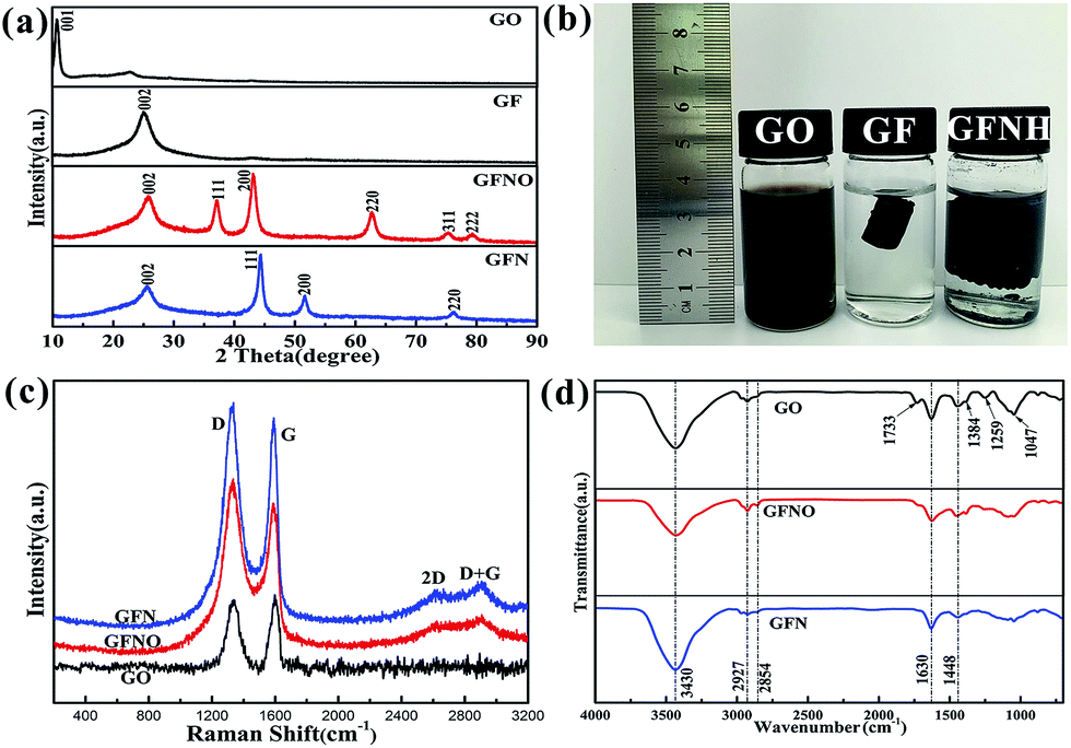 | ||
| Fig. 4 (a) XRD patterns of GO, GF, GFNO and GFN; (b) photographs of GO, GF and GFNH aqueous solutions; (c) Raman spectra of GO, GFNO and GFN, (d) FTIR spectra of GO, GFNO and GFN. | ||
The structural changes in the carbon framework were investigated by Raman, and the spectra of GO, GFN and GFNO are shown in Fig. 4c. For GO, there are two noticeable peaks at 1338 cm−1 and 1597 cm−1, corresponding to the D and G bands, respectively. The D band is ascribed to the vibrations of sp3 carbon atoms in disordered graphite, and the G band is attributed to the in-plane vibrations of sp2 carbon atoms in a 2D hexagonal lattice. It is clear that the D to G band intensity ratios (ID/G) of GFN and GFNO (1.07 and 1.178, respectively) are both higher than that of GO (0.876), suggesting that the reduction of GO leads to the formation of new and smaller sp2 domains.32 In addition, compared with GO, the D and G bands of GFN red-shift to 1323 cm−1 and 1590 cm−1, and those of GFNO red-shift to 1333 cm−1 and 1590 cm−1.33 The red-shift indicates the restoration of the conjugated π system, because the conjugated double bonds in graphene have lower resonant vibration frequencies than the isolated double bonds formed during the oxidation. It is worth noting that GFN shows a lower ID/G and a larger red-shift of the D band compared with GFNO, which indicates that less localized sp3 defects exist in GFN within the sp2 carbon network, as well as a higher degree of reduction, due to the hydrogen reduction during the calcination process.
As shown in Fig. 4d, the structural components of GO, GFNO and GFN were identified by FTIR spectroscopy. The characteristic bands of GO correspond to oxygen-containing functional groups, including O–H (3430 cm−1 and 1448 cm−1), C![[double bond, length as m-dash]](https://www.rsc.org/images/entities/char_e001.gif) O (1733 cm−1), carboxyl C–O (1384 cm−1), epoxy C–O (1259 cm−1) and alkoxy C–O (1047 cm−1), as well as to C–H (2927 cm−1 and 2854 cm−1) and CC (1630 cm−1) bonds.34,35 However, for GFNO, obtained after reduction of GO, the oxygen-containing groups, such as CO, carboxyl C–O and epoxy C–O, clearly display weaker bands than in GO, and some are even no longer present. As for GFN, all the oxygen-containing functional groups almost vanish after reduction, which reflects that the degree of reduction in GFN is higher than in GFNO, and that Ni(OH)2 can be converted to Ni by calcination under hydrogen.
O (1733 cm−1), carboxyl C–O (1384 cm−1), epoxy C–O (1259 cm−1) and alkoxy C–O (1047 cm−1), as well as to C–H (2927 cm−1 and 2854 cm−1) and CC (1630 cm−1) bonds.34,35 However, for GFNO, obtained after reduction of GO, the oxygen-containing groups, such as CO, carboxyl C–O and epoxy C–O, clearly display weaker bands than in GO, and some are even no longer present. As for GFN, all the oxygen-containing functional groups almost vanish after reduction, which reflects that the degree of reduction in GFN is higher than in GFNO, and that Ni(OH)2 can be converted to Ni by calcination under hydrogen.
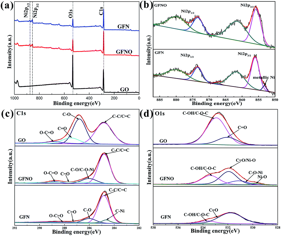
The surface composition of GO, GFNO and GFN were analyzed by XPS (Fig. 5). In Fig. 5a, the wide scan XPS spectra of the three products show that GFNO and GFN are both composed of C, O and Ni elements, and no other elements are detected. Fig. 5b shows the two peaks corresponding to Ni 2p3/2 and Ni 2p1/2 (855.73 and 873.43 eV) with two satellite peaks (861.51 and 879.76 eV), respectively.36 It is worth noting that there is a shoulder peak at 853 eV on the Ni 2p spectrum of GFN, which is attributed to metallic Ni in the C–Ni bond.37 Correspondingly, the C 1s spectrum of GFN (Fig. 5c) shows an apparent peak at 284.6 eV, assigned to the carbon from nickel carbide.38 These two peaks demonstrate the existence of C–Ni bonds in GFN. In addition, the four peaks at 284.8 eV, 286.81 eV, 287.5 eV and 288.80 eV in the C 1s spectra are ascribed to C–C/CC, C–O, CO and O–CO, respectively.28,32 Fig. 5d reveals the O 1s XPS spectrum of GO, GFNO and GFN. The deconvoluted spectrum of GO consists of two peaks at 531.9 eV and 532.9 eV, corresponding to CO and C–OH/C–O–C groups.39 For GFNO, there are two additional peaks at 529.7 eV and 530.2 eV. In general, the peak at 529.7 eV is assigned to Ni–O groups, and the peak at 531.9 eV is ascribed to CO or to the shoulder peak of O 1s of Ni–O.28,40,41 Upon comparing with the peak at 532.9 eV in the GO spectrum, it can be concluded that the content of C–OH/C–O–C groups in GFNO is much smaller, indicating the replacement of hydrogen in hydroxyl groups or a possible ring opening reaction of the epoxy groups after introducing Ni2+, which results in the formation of a C–O–Ni linkage. This is consistent with the results obtained by first-principles calculations.41 The peak centered at 530.2 eV is attributed to the possible formation of C–O–Ni bonds.40,42 For GFN, the content of CO and C–OH/C–O–C groups is much smaller than those of GO, indicating that the Ni nanoparticles assist in the removal of the CO and C–OH/C–O–C groups.39 Table 1 shows the atomic percentages of C, O and Ni for GO, GFNO and GFN. These percentages further confirm the successful reduction of GO to give GFNO and GFN, and are consistent with the FTIR results. In summary, all of the abovementioned analyses confirm that GF, GFNO and GFN were successfully synthesized.
 | ||
| Fig. 5 (a) XPS spectra of the survey scans of GO, GFN and GFNO, (b) Ni 2p spectrum of GFNO and GFN, (c) C 1s spectrum, and (d) O 1s spectrum of GO, GFNO and GFN. | ||
| Sample | C (%) | O (%) | Ni (%) |
|---|---|---|---|
| GO | 54.30 | 45.70 | — |
| GFNO | 43.67 | 28.80 | 27.53 |
| GFN | 43.40 | 22.76 | 33.84 |
The electromagnetic parameters, presented in Fig. 6, were measured to evaluate the MA properties. The real permittivity (ε′) and permeability (μ′) represent the storage of the microwave energy, whereas the imaginary permittivity (ε′′) and permeability (μ′′) represent the loss capability of the electric and magnetic energy, respectively. The MA properties are determined by the complex permeability (μr = μ′ − jμ′′) and the complex permittivity (εr = ε′ − jε′′), as well as the dielectric tangent loss (tanδε = ε′′/ε′) and the magnetic tangent loss (tanδμ = μ′′/μ′).
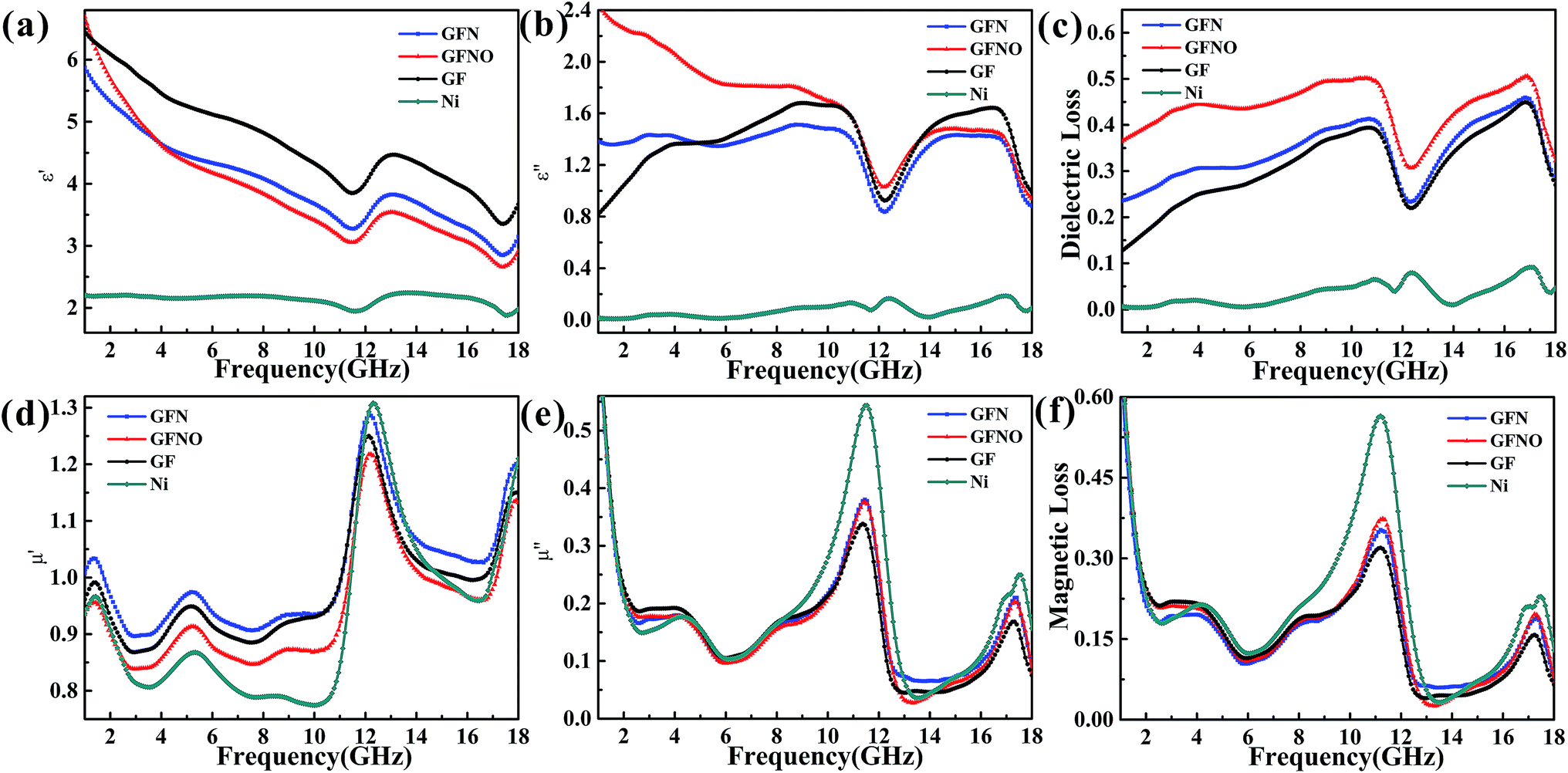 | ||
| Fig. 6 Complex permittivity (a and b); complex permeability (d and e); and dielectric and magnetic loss (c and f) between 1 and 18 GHz for GFN/wax, GFNO/wax, GF/wax and Ni/wax samples. | ||
In Fig. 6a, it can be seen that the ε′ of GF, GFN and GFNO decrease as frequency increases, whereas that of Ni nanoparticles is maintained constant with only a slight fluctuation. It is clear that GF exhibits a higher real permittivity than the rest, which is attributed to the high conductivity due to the increased physical contact between the conductive graphene sheets. Moreover, the ε′ value of GFNO is higher than that of GFN at 1 GHz due to the intrinsic properties of NiO (the static dielectric constant of bulk NiO is 10.31 or 11.75).14 Subsequently, the ε′ value of GFNO rapidly decreases as the frequency increases. However, it is clear that the ε′′ versus frequency curves of GF, GFN and GFNO show conspicuous undulation and there are two resonance peaks at the same frequency (Fig. 6b), indicating that GF, GFN and GFNO exhibit the same relaxation mechanism.43 Furthermore, Fig. 6c shows that the dielectric tangent loss of GFNO is higher than that of GFN. NiO is a typical p-type semiconductor and a dielectric material with a high static dielectric constant. After NiO nanoparticles bond to the graphene foam, GFNO exhibits a high dielectric loss owing to the high electrical conductivity of graphene and the high dielectric constant of NiO. Consequently, the dielectric tangent loss of GFNO is higher than that of GFN.
In general, the dielectric loss can be investigated by the Debye dipole theory, and the real and imaginary permittivity can be expressed by the following equations:44
 | (1) |
 | (2) |
The magnetic loss is another important aspect for MA properties. As shown in Fig. 6d and e, the μ′ and μ′′ values of GFN are high due to the magnetic metallic Ni NPs. It is obvious that the μ′–f and μ′′–f curves fluctuate as the frequency increases and show some resonance peaks. The magnetic tangent loss (tanδμ) represents the capacity of magnetic materials for absorbing microwave energy and is an important factor for evaluating the microwave absorption behavior. Fig. 6f shows the magnetic tangent loss versus frequency for these four samples. Generally, magnetic loss is due to eddy current effects and natural resonance.18 If loss through eddy currents is the only mechanism of magnetic loss, the values of μ′′(μ′)−2f−1 should remain constant throughout a range of frequencies.45–47 Fig. 7 shows the μ′′(μ′)−2f−1–f curves of these four samples. For GFN, the μ′′(μ′)−2f−1 values are constant in the 6–11 GHz and 13–18 GHz ranges, indicating that the loss is caused by eddy current effects instead of natural resonance. In a different frequency range, the μ′′(μ′)−2f−1–f curve shows fluctuations, illustrating that both eddy current effects and natural resonance cause magnetic loss in these frequency range.
 | ||
| Fig. 7 μ′′(μ′)−2f−1–f curves of GFN, GFNO, GF and Ni NPs. | ||
The natural resonance can be described by the following equations:
| 2πfr = rHa | (3) |
| Ha = 4|K1|/3μ0Ms | (4) |
According to the transmission line theory, the RL of these specimens can be calculated by the following formulae:51,52
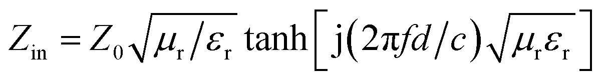 | (5) |
|
RL (dB) = 20log|(Zin − Z0)/(Zin − Z0)|
| (6) |
The calculated RL values of GF, GFN, GFNO and Ni nanoparticles are shown in Fig. 8 and 9. Also, the RL curves of these four samples with different thickness are shown in Fig. 8. For a thickness of 2.6 mm, the maximum RL of GFN reaches −29.2 dB at 16.9 GHz and the bandwidth below −10 dB is 5 GHz. For GF, the maximum RL is only −22.2 dB and the bandwidth of effective absorption (RL < −10 dB) is 4.6 GHz. With a thickness of 3.5 mm, the RL of GFN increases to a maximum of −37.6 dB at 11.28 GHz. Furthermore, the RL peak shifts to low frequencies as the sample thickness increases, which is consistent with previous reports.53,54 When the thickness increases to 5 mm, the absorption intensity and effective absorption bandwidth (RL < −10 dB) of GFN both increase and exhibit superior microwave absorption with respect to the other samples, which can be ascribed to the better impedance matching characteristics of GFN.
 | ||
| Fig. 8 RL versus frequency curves of samples with different thickness: (a) 2.6 mm, (b) 3.5 mm and (c) 5 mm. | ||
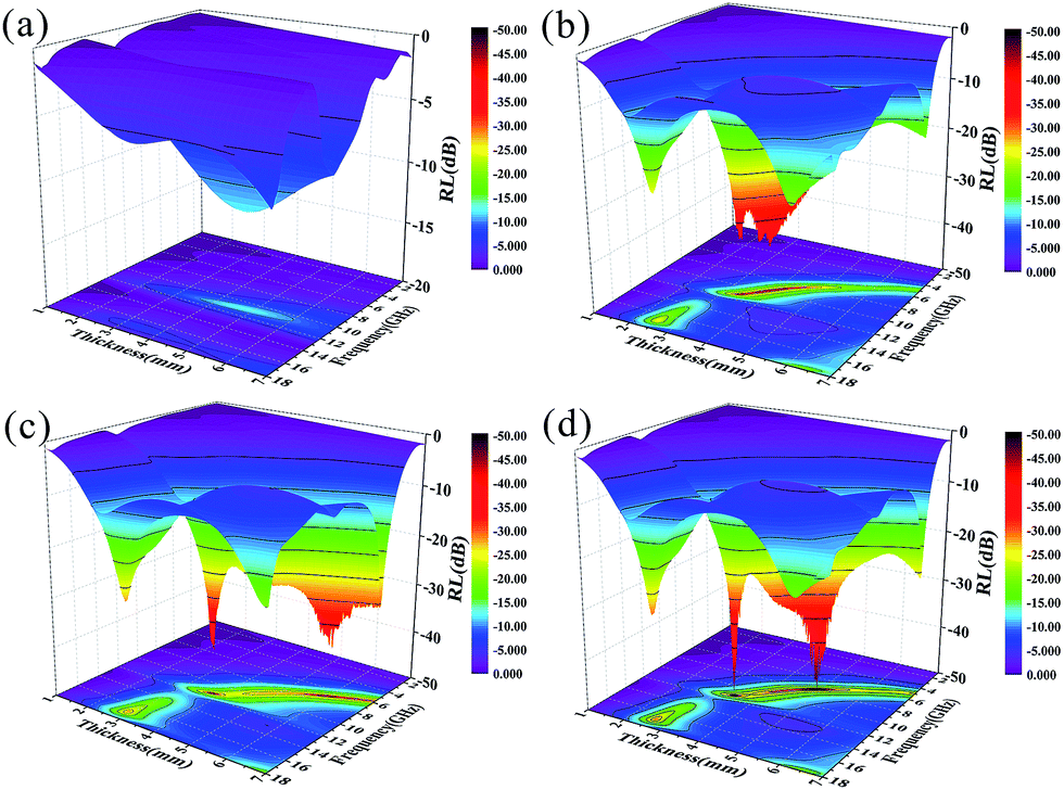 | ||
| Fig. 9 3D plots of RL versus frequency and thickness for (a) Ni NPs, (b) GF, (c) GFNO and (d) GFN. | ||
Fig. 9 shows the 3D plots of RL versus frequency and thickness for these four samples. In Fig. 9a, we can clearly see that pure Ni nanoparticles exhibit the worst MA properties due to poor impedance matching and low content (the filler content is only 1 wt%). As shown in Fig. 9b–d, the 3D plot of GF reveals the same broad absorption band below −30 dB for GFN and GFNO, which is due to defect polarization and electron polarization of the residual defects and to the horizontal alignment of graphene.55,56 The maximum RL of GFN (Fig. 9d) was −49 dB at 11.5 GHz and 7.8 GHz, with a thickness of 3.4 mm and 4.9 mm, respectively, which is much higher than the maximum RL of GF. In addition, as shown in Table 2, compared with other materials from previous studies, such as graphene–Ni composites,6 laminated magnetic graphene13 and FeCo/graphene hybrids, the GFN composite shows good MA properties with low content, high RL and a broad absorption bandwidth, which is attributed to its 3D structure and the better impedance matching characteristics between Ni nanoparticles and graphene. As shown in the 2D plane projection, GFN shows better MA properties than GFNO with low-thickness samples, in the thickness range of 1–5 mm, both in terms of absorption intensity and effective absorption bandwidth (RL < −10 dB), which can be attributed to the better matching of magnetic Ni nanoparticles and to the conductive graphene network.
| Material | Maximum RL | Absorption bandwidth (RL < −10 dB) | Content | Reference |
|---|---|---|---|---|
| GFN | −49 dB at 11.5 GHz | 8.5–12.5 GHz | 1 wt% | This work |
| Graphene–Ni composite | −42 dB at 17.6 GHz | 15.4–18 GHz | 30 wt% | 6 |
| rGO–Fe3O4 | −26.4 dB at 5.3 GHz | 4.5–6.5 GHz | 40 wt% | 13 |
| FeCo/graphene hybrid | −40.2 dB at 8.9 GHz | 7.5–11 GHz | 50 wt% | 19 |
In summary, GFN exhibits better MA properties than GF, GFNO and Ni NPs, which may be explained by the following reasons. First, the 3D structure of graphene foam gives rise to multiple reflections and scattering of the electromagnetic waves. In this process, the electromagnetic energy is transformed into heat or other forms of energy, and it is ultimately dissipated, as shown in Fig. 10a. Second, it is generally known that the RL can be affected by the impedance matching characteristics. In GFN, the synergistic effect between graphene foam and Ni NPs, with an efficient complementarity between the complex permeability and permittivity, imparts superior impedance matching characteristics with respect to GFNO, GF and Ni NPs. Third, natural resonance, eddy current effects, and interfacial and dipole polarization originated from the magnetic Ni NPs in graphene foam, enhance microwave absorption. In addition, the defects and groups in rGO introduce defect polarization, electron polarization and the associated relaxation (Fig. 10b), all of which also contribute to enhance the MA properties of GFN.
 | ||
| Fig. 10 (a) Microwave attenuation mechanism for the 3D foam structure and Ni NPs in GFN; (b) defect polarization and electric dipole polarization of the rGO sheets in GFN. | ||
Conclusions
In summary, GFN, designed to improve the MA properties, was fabricated by a hydrothermal method, followed by a calcination process. Due to the 3D structure of graphene foam and the evenly dispersed nickel nanoparticles, GFN shows an enhanced attenuation of electromagnetic waves and impedance matching characteristics. Under the synergistic effect of multiple polarization and resonance, the GFN/wax sample with a GFN loading of only 1 wt% exhibited good MA properties. For the GFN/wax sample with a thickness of 2.6 mm, the maximum RL was −29.2 dB at 16.9 GHz, and the bandwidth below −10 dB is 5 GHz. As thickness increases, the maximum RL value shifts to a low frequency region and reaches to −49 dB with a thickness of 4.9 mm and 3.4 mm. Compared with the other four samples, GFN exhibits the best MA properties, both in terms of high absorption intensity and broader effective absorption bandwidth (RL < −10 dB). Therefore, the 3D graphene foam/Ni nanoparticle composite, with a strong absorption and lightweight properties, is a remarkably promising microwave absorption material.Acknowledgements
This study was financially supported by the National Natural Science Foundation of China (Grants 51671013). The authors thank the Aerospace Materials and the Technology Research Institute for their support.Notes and references
- Y. Lin, L. Xu, Z. Y. Jiang, H. L. Li, Z. X. Xie and L. S. Zheng, RSC Adv., 2015, 5, 70849 RSC.
- L. Wang, Y. Huang, C. Li, J. Chen and X. Sun, Phys. Chem. Chem. Phys., 2015, 17, 2228 RSC.
- M. Fu, Q. Jiao, Y. Zhao and H. Li, J. Mater. Chem. A, 2014, 2, 735 CAS.
- A. K. Das, S. Sahoo, P. Arunachalam, S. Zhang and J.-J. Shim, RSC Adv., 2016, 6, 107057 RSC.
- Z. Lu, L. Ma, J. Tan, H. Wang and X. Ding, Nanoscale, 2016, 8, 16684 RSC.
- Z. Zhu, X. Sun, G. Li, H. Xue, H. Guo, X. Fan, X. Pan and J. He, J. Magn. Magn. Mater., 2015, 377, 95 CrossRef CAS.
- C. Hu, Z. Mou, G. Lu, N. Chen, Z. Dong, M. Hu and L. Qu, Phys. Chem. Chem. Phys., 2013, 15, 13038 RSC.
- Z. Y. Peijiang Liu, J. Zhou, Z. Yangad and L. B. Kong, J. Mater. Chem. C, 2016, 4, 9738 RSC.
- C. Wang, X. Han, P. Xu, X. Zhang, Y. Du, S. Hu, J. Wang and X. Wang, Appl. Phys. Lett., 2011, 98, 072906 CrossRef.
- X. Zhao, Z. Zhang, L. Wang, K. Xi, Q. Cao, D. Wang, Y. Yang and Y. Du, Sci. Rep., 2013, 3, 3421 Search PubMed.
- G. Pan, J. Zhu, S. Ma, G. Sun and X. Yang, ACS Appl. Mater. Interfaces, 2013, 5, 12716 CAS.
- X. Jian, B. Wu, Y. Wei, S. X. Dou, X. Wang, W. He and N. Mahmood, ACS Appl. Mater. Interfaces, 2016, 8, 6101 CAS.
- X. Sun, J. He, G. Li, J. Tang, T. Wang, Y. Guo and H. Xue, J. Mater. Chem. C, 2013, 1, 765 RSC.
- L. Wang, Y. Huang, X. Sun, H. Huang, P. Liu, M. Zong and Y. Wang, Nanoscale, 2014, 6, 3157 RSC.
- Y. Qing, D. Min, Y. Zhou, F. Luo and W. Zhou, Carbon, 2015, 86, 98 CrossRef CAS.
- Z. Zhu, X. Sun, H. Xue, H. Guo, X. Fan, X. Pan and J. He, J. Mater. Chem. C, 2014, 2, 6582 RSC.
- X.-J. Zhang, G.-S. Wang, Y.-Z. Wei, L. Guo and M.-S. Cao, J. Mater. Chem. A, 2013, 1, 12115 CAS.
- P. Liu, Y. Huang, J. Yan, Y. Yang and Y. Zhao, ACS Appl. Mater. Interfaces, 2016, 8, 5536 CAS.
- X. Li, J. Feng, Y. Du, J. Bai, H. Fan, H. Zhang, Y. Peng and F. Li, J. Mater. Chem. A, 2015, 3, 5535 CAS.
- M. Verma, A. P. Singh, P. Sambyal, B. P. Singh, S. K. Dhawan and V. Choudhary, Phys. Chem. Chem. Phys., 2015, 17, 1610 RSC.
- X. J. Zhang, G. S. Wang, W. Q. Cao, Y. Z. Wei, J. F. Liang, L. Guo and M. S. Cao, ACS Appl. Mater. Interfaces, 2014, 6, 7471 CAS.
- Y. Zhang, Y. Huang, T. Zhang, H. Chang, P. Xiao, H. Chen, Z. Huang and Y. Chen, Adv. Mater., 2015, 27, 2049 CrossRef CAS PubMed.
- X. F. Zhang, X. L. Dong, H. Huang, Y. Y. Liu, W. N. Wang, X. G. Zhu, B. Lv, J. P. Lei and C. G. Lee, Appl. Phys. Lett., 2006, 89, 053115 CrossRef.
- S. H. A. R. E. Offema, J. Am. Chem. Soc., 1958, 80, 1339 CrossRef.
- M. Yu, J. P. Chen, Y. X. Ma, J. D. Zhang, J. H. Liu, S. M. Li and J. W. An, Appl. Surf. Sci., 2014, 314, 1000 CrossRef CAS.
- M. Yu, P. R. Liu, Y. J. Sun, J. H. Liu, J. W. An and S. M. Li, J. Inorg. Mater., 2012, 27, 89 CrossRef CAS.
- X. Wu, B. Wang, S. Li, J. Liu and M. Yu, RSC Adv., 2015, 5, 33438 RSC.
- X. Meng, J. Zhu, H. Bi, Y. Fu, Q. Han and X. Wang, J. Mater. Chem. A, 2015, 3, 21682 CAS.
- S. Rajendran, M. M. Khan, F. Gracia, J. Qin, V. K. Gupta and S. Arumainathan, Sci. Rep., 2016, 6, 31641 CrossRef CAS PubMed.
- R. Saravanan, V. K. Gupta, E. Mosquera and F. Gracia, J. Mol. Liq., 2014, 198, 409–412 CrossRef CAS.
- X. Q. Xie, S. Q. Chen and B. Sun, ChemSusChem, 2015, 8, 2948–2955 CrossRef CAS PubMed.
- J. Balamurugan, T. D. Thanh, S.-B. Heo, N. H. Kim and J. H. Lee, Carbon, 2015, 94, 962 CrossRef CAS.
- G. S. Wang, Y. Wu, Y. Z. Wei, X. J. Zhang, Y. Li, L. D. Li, B. Wen, P. G. Yin, L. Guo and M. S. Cao, ChemPlusChem, 2014, 79, 375 CrossRef CAS.
- L. J. Xie and F. Y. Su, chemsuschem, 2015, 8, 2917 CrossRef CAS PubMed.
- M. Zong, Y. Huang, N. Zhang and H. Wu, J. Alloys Compd., 2015, 644, 491 CrossRef CAS.
- Z. Zhang, A. Matsubayashi, B. Grisafe, J. U. Lee and J. R. Lloyd, Mater. Chem. Phys., 2016, 170, 175 CrossRef CAS.
- J. F. Blandez, I. Esteve-Adell, A. Primo, M. Alvaro and H. García, J. Mol. Catal. A: Chem., 2016, 412, 13 CrossRef CAS.
- W. Zhang, Y. Li, X. Zeng and S. Peng, Sci. Rep., 2015, 5, 10589 CrossRef CAS PubMed.
- A. K. Ray, R. K. Sahu, V. Rajinikanth, H. Bapari, M. Ghosh and P. Paul, Carbon, 2012, 50, 4123 CrossRef CAS.
- X. Liu, W. Liu, M. Ko, M. Park, M. G. Kim, P. Oh, S. Chae, S. Park, A. Casimir, G. Wu and J. Cho, Adv. Funct. Mater., 2015, 25, 5799 CrossRef CAS.
- G. Zhou, D. W. Wang, L. C. Yin, N. Li, F. Li and H. M. Cheng, ACS Nano, 2012, 6, 3214 CrossRef CAS PubMed.
- X. Feng, J. Zhou, L. Wang, Y. Li, Z. Huang, S. Chen, Y. Ma, L. Wang and X. Yan, New J. Chem., 2015, 39, 4026 RSC.
- X. Zhang, G. Ji, W. Liu, B. Quan, X. Liang, C. Shang, Y. Cheng and Y. Du, Nanoscale, 2015, 7, 12932 RSC.
- M. Q. Ning, M. M. Lu, J. B. Li, Z. Chen, Y. K. Dou, C. Z. Wang, F. Rehman, M. S. Cao and H. B. Jin, Nanoscale, 2015, 7, 15734 RSC.
- F. Wen, F. Zhang and Z. Liu, J. Phys. Chem. C, 2011, 115, 14025 CAS.
- Q. Liu, X. Xu, W. Xia, R. Che, C. Chen, Q. Cao and J. He, Nanoscale, 2015, 7, 1736 RSC.
- J. Liu, M. S. Cao, Q. Luo, H. L. Shi, W. Z. Wang and J. Yuan, ACS Appl. Mater. Interfaces, 2016, 8, 22615 CAS.
- C. L. Zhu, M. L. Zhang, Y. J. Qiao, G. Xiao, F. Zhang and Y. J. Chen, J. Phys. Chem. C, 2010, 114, 16229 CAS.
- X. F. Liu, X. R. Cui, Y. X. Chen, X. J. Zhang, R. H. Yu, G. S. Wang and H. Ma, Carbon, 2015, 95, 870 CrossRef CAS.
- F. Ma, J. Ma, J. Huang and J. Li, J. Magn. Magn. Mater., 2012, 324, 205 CrossRef CAS.
- W. She, H. Bi, Z. Wen, Q. Liu, X. Zhao, J. Zhang and R. Che, ACS Appl. Mater. Interfaces, 2016, 8, 9782 CAS.
- M. Liu, G. Lv, G. Chen, Y. Qin, P. Sun, K. Zhou, X. Xing and C. He, RSC Adv., 2016, 6, 102472 RSC.
- N. Li, M. Cao and C. Hu, J. Mater. Chem., 2012, 22, 18426 RSC.
- J. Liu, Y. Feng and T. Qiu, J. Magn. Magn. Mater., 2011, 323, 3071 CrossRef CAS.
- W. L. Song, M. S. Cao, M. M. Lu, J. Yang, H. F. Ju, Z. L. Hou, J. Liu, J. Yuan and L. Z. Fan, Nanotechnology, 2013, 24, 115708 CrossRef PubMed.
- N. Yousefi, X. Sun, X. Lin, X. Shen, J. Jia, B. Zhang, B. Tang, M. Chan and J. K. Kim, Adv. Mater., 2014, 26, 5480 CrossRef CAS PubMed.
Footnote |
| † Electronic supplementary information (ESI) available. See DOI: 10.1039/c6ra27435h |
| This journal is © The Royal Society of Chemistry 2017 |