
 Open Access Article
 This Open Access Article is licensed under a
 Creative Commons Attribution 3.0 Unported Licence
Magnetic modification of GaSe monolayer by absorption of single Fe atom
Yihong Lu ,
Congming Ke,
Mingming Fu,
Wei Lin,
Chunmiao Zhang,
Ting Chen,
Heng Li,
Junyong Kang,
Zhiming Wu* and
Yaping Wu*
,
Congming Ke,
Mingming Fu,
Wei Lin,
Chunmiao Zhang,
Ting Chen,
Heng Li,
Junyong Kang,
Zhiming Wu* and
Yaping Wu*
Fujian Provincial Key Laboratory of Semiconductors and Applications, Collaborative Innovation Center for Optoelectronic Semiconductors and Efficient Devices, Department of Physics, Xiamen University, Xiamen 361005, P. R. China. E-mail: ypwu@xmu.edu.cn; zmwu@xmu.edu.cn; Fax: +86-592-2181366; Fax: +86-592-2180858
First published on 16th January 2017
Abstract
Group-IIIA metal-monochalcogenides have attracted increasing interests due to their optoelectronic and spin electronic properties. Achieving the modification of their magnetism is desirable for device applications. In our work, structural, electronic, and magnetic properties of the Fe adsorbed GaSe monolayer are studied systematically using density functional theory (DFT). It is found that there is a strong orbit coupling effect between Fe and the vicinal Ga and Se atoms, resulting in a half-metallicity with a 100% spin polarization. The magnetic moments of the nearest neighbour Ga and Se atoms are −0.004 μB and −0.178 μB, respectively, demonstrating an antiferromagnetic coupling with the adsorbed Fe atom. Meanwhile, the induced majority and minority spin states are inclined to distribute on the Se and Ga atoms separately. The hybridization of Fe-3d, Se-4p, and Ga-4p orbitals is responsible for the induced magnetic moments and spin polarization in the nonmagnetic GaSe monolayer. These investigations shed light on understanding the electronic and magnetic properties of the ferromagnetic/GaSe adsorption system, which offer some references for the design and construction of two-dimensional spin nanostructures.
1 Introduction
As the first prototype of two-dimensional (2D) materials, graphene has been extensively studied for its unique electrical, thermal, mechanical, and chemical properties.1–3 However, its intrinsic bottleneck, the lack of band gap, essentially blocks its application in the traditional emitting devices. Besides the efforts that have been made for opening the band gap in graphene,4,5 more researchers are trying to exploit other 2D materials with various band gaps to meet the multiple demands of device applications.6–9Recently, a new kind of layered semiconductor material, group-IIIA metal-monochalcogenides MX (M = Ga, In; X = S, Se, Te), have aroused increasing interests due to their optoelectronic applications.10,11 GaSe nanoslabs made by mechanical exfoliation show excellent photoresponse property. The responsivity, corresponding quantum efficiency, and on–off ratios can reach 2.8 A W−1, 1367%, and 103, respectively, which are superior to counterpart of other 2D materials such as MoS2 and graphene.10,12,13 Besides the electronic and optoelectronic devices, group-IIIA metal-monochalcogenides 2D materials also possess normal spin electronic properties. Their unique band structure removes the degeneracies between orbital states and thereby allows generation and preservation of a high degree of spin polarization under nonresonant optical pumping.14,15 The high spin polarization and long spin relaxation time open up a potential application on spintronic and magnetoelectric fields. In order to realize the controllable on the magnetization to satisfy the request of design goals, people further put emphasis on the modification of their intrinsic spin properties by applying an external stress,16 modulating the chemical composition,16 or employing charge doping.17 The reactive crystal structure of group-IIIA metal-monochalcogenides 2D materials could provide a rich playground for functionalizations at nanoscale. Doping with foreign atoms and creating vacancy defects, have been reported to produce high spin polarization in GaSe monolayer (ML), resulting in itinerant ferromagnetism and half-metallicity.18,19 Relatively, the electronic and magnetic properties modified by adsorption of the foreign atoms are rarely reported. Because of the high electronic polarizability, high Curie temperature, and easy preparation, ferromagnetic materials, such as Fe, Co, and Ni, become the best option of adsorbates.20–22 By introducing the ferromagnetic atoms on the surface of metal-monochalcogenides ML, their magnetic and electronic properties can be modified conveniently.
In this work, the structural, electronic and magnetic properties of Fe adsorbed GaSe ML are investigated systematically by using the density functional theory. Based on the most stable site determined by the adsorption energies, spin-resolved band structures and the electronic total density of states (TDOS) are calculated to study the orbit coupling effect and magnetic property of Fe/GaSe system. The deformation charge densities as well as the partial spin charge distribution are further analyzed, which show the interaction between Fe and underlying GaSe, and reveal the physical mechanism for the induced magnetic moments and spin polarization in nonmagnetic GaSe ML.
2 Methods and calculation details
The geometric and electronic structures of pristine and Fe-adsorbed GaSe (denoted as Fe/GaSe) MLs are analyzed using the plane-wave DFT, as implemented in the Vienna ab initio simulation package (VASP)23–25 code with the projector augmented wave (PAW) basis sets. In order to avoid the adatom–adatom interaction and interlayer interaction, a 3 × 3 supercell (18 Ga and 18 Se atoms) and a 25 Å vacuum layer along the z direction are used for the GaSe and Fe/GaSe MLs. Valence electron configurations of Ga, Se and Fe atoms are 4s24p1, 4s24p4 and 3d64s2, respectively. The generalized gradient approximation (GGA) with Perdew–Burke–Ernzerhof (PBE) parameterization26 is employed as the exchange–correlation function. The Brillouin zone is sampled with a 9 × 9 × 1 Monkhorst–Pack grid of k points, and a cutoff energy of 350 eV is used for the plane waves. All atomic degrees of freedom, including lattice parameters, are fully relaxed with electronic iteration convergences of 0.01 eV Å−1 and 1 × 10⁻⁶ eV for force and energy, respectively.3 Results and discussion
We first investigate the geometric configuration of the 3 × 3 GaSe supercell, as shown in Fig. 1(a). The planar projection of pristine GaSe exhibits an ideal hexagonal honeycomb structure, similar to that of graphene and some of other 2D nanomaterials. The optimized lattice constant in present work is 3.82 Å, well consistent with previous result.27,28 The lengths of Ga–Ga and Ga–Se bonds are about 2.47 Å and 2.50 Å, and the Se–Ga–Se angle between the nearest-neighbour Se atoms are about 99.5°.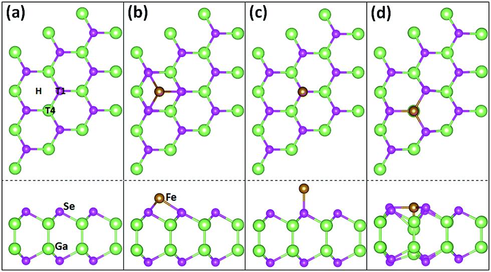 | ||
| Fig. 1 Sketch maps. Top and side views of the relaxed GaSe ML (a), and of the relaxed Fe/GaSe models with a Fe adatom locating on (b) H, (c) T1, and (d) T4 sites of GaSe, respectively. | ||
Considering the geometric symmetry of GaSe surface, three high symmetrical sites, H, T1, and T4, which represent the hollow site, the top site of Se atom and the top site of Ga atom, respectively, are selected as the possible stable adsorption sites, as shown in Fig. 1(b–d). The adsorption energy of Fe atom is defined as Ead = EGaSe + EFe − EFe/GaSe, where EGaSe, EFe, and EFe/GaSe are the energies of the pristine GaSe, the Fe atom, and the Fe/GaSe system, respectively. System can be stable if Ead is positive. The calculated results suggest that the adsorption energies of Fe on H site, T1 site, and T4 site are 1.08 eV, 0.59 eV and 2.20 eV, respectively. The largest adsorption energy for Fe adatom on T4 site means that the top site of Ga atom is the most stable adsorption site for a Fe adatom. Examining the atomic coordinates in the models, the positions of Ga and Se atoms are found almost unchanged for the adsorption on H and T1 sites, but are strongly changed for the adsorption on T4 site. Besides, as the Fe adatom on the T4 site, the Fe–Ga and Fe–Se bond lengths are respectively 2.14 Å and 2.38 Å, as listed in Table 1, both smaller than the counterpart of other two cases. Shorter bond length normally means a more significant wave function overlapping and a stronger interactions between atoms. This infers that the interactions between Fe adatom and its nearest neighbour atoms are stronger when the Fe atom absorbing on T4 site than that on H and T1 sites. We can also find out that the Ga–Se bond length near the Fe adatom is larger than that of pristine GaSe ML, indicating a relative weaker interaction between adjacent Ga and Se atoms after the adsorption.
| Fe/GaSe | Fe–Se | Fe–Ga |
|---|---|---|
| H | 2.53 | — |
| T1 | 2.40 | — |
| T4 | 2.38 | 2.14 |
To ascertain the electronic properties of Fe/GaSe system, the spin-resolved energy band structures and total density of states (TDOS) are calculated, with the comparison of that of pristine GaSe, as shown in Fig. 2. Pristine GaSe exhibits an indirect band gap as the conduction band minimum (CBM) is locating at the Γ point while the valence band maximum (VBM) is locating between the Γ and M points (Fig. 2a), consistent with the previous report.18 The calculated band gap is 1.83 eV, which agrees well with the previous studies.29 Both the energy band and TDOS show a coincident distribution for the majority and minority spin states (Fig. 2d), indicative of a non-magnetic ground state. As the adsorption of a Fe atom, the energy band splits into uncoincident majority and minority spin channels (Fig. 2b and c). The VBM moves toward Γ point, producing a direct-band-gap in the system. Some new energy levels appear near the CBM and VBM, coupling with the original bands, and narrowed the energy gap by about 0.55 eV. Compared with the TDOS of pristine GaSe, the Fermi level of Fe/GaSe moves toward higher energy (Fig. 2e). Bader charge analysis shows that about 0.347 e and 0.004 e charge transfer respectively from the Fe adatom and the three surrounding Se atoms to the nearest neighbour Ga atom (Table 2), generating n-type doping. Two impurity bands locate in the energy gap near the Fermi level and contribute only to the minority spin channel (Fig. 2c and e), claiming a half-metallicity with a 100% spin polarization for the Fe/GaSe system. Half-metallicity in the adsorbed systems of group-IIIA metal-monochalcogenides has rarely been reported before. As for doped systems, GaSe ML doped with Ti, Cr, and Ni also exhibits half-metallic features, but for Fe doped GaSe ML, no spin polarization was found in the Fermi level.19 In the case of doped GaS ML, despite of the occupation of spin states close to the CBM and VBM for some dopant elements (such as Cr and Co), but half-metallic property was still absent because of the lack of polarized spin channel in the Fermi level.30 Consequently, the Fe/GaSe adsorbed ML may be a better choice than Fe doped systems to realize half-metallicity for spintronic applications.
 | ||
| Fig. 2 Energy band structures and TDOS of (a and d) the pristine GaSe, and (b, c and e) a Fe atom adsorbed GaSe MLs (b and c are the majority and the minority spin band structures, respectively). | ||
| Fe | Se | Ga | |
|---|---|---|---|
| ΔQ (e) | −0.347 | −0.040 | 0.446 |
| Magnetic (μB) | 2.122 | −0.004 | −0.178 |
In order to find out the origin of the polarized spin states, aligning partial density of states (PDOS) of the Fe and its nearest neighbour atoms are calculated, as shown in Fig. 3. Electronic states of the adsorbed Fe atom exhibit a significant domination in the minority spin channel at CBM and in the majority spin channel at VBM, ranging from 0.75 to 0.86 eV and from −0.83 to −0.55 eV, respectively. The contribution mainly comes from its 3d states, while the 4s states play a trivial role. As for the nearest Se atom, 4p states contribute obviously in the majority spin channel at VBM, ranging from −0.83 to −0.55 eV, while the 4s states play a minor role. Different from that of the Se atom, the electronic states of the nearest Ga atom contribute less at the VBM, but more in the majority spin channel at the vicinity of CBM from both the 4s and 4p states. Besides of the coupling states at the VBM and CBM, some spin-polarized impurity levels present near the Fermi level for the Fe, and its nearest neighbour atoms. They occupy only the minority spin channel across the Fermi level, resulting in a half-metallic conductive property. One can see that the PDOS of Se 4p orbitals and Ga 4s and 4p orbitals match consistently with Fe 3d orbitals both at the VBM and near the Fermi level, which suggests an efficient overlapping of wave functions between Fe and the nearest neighbour atoms.
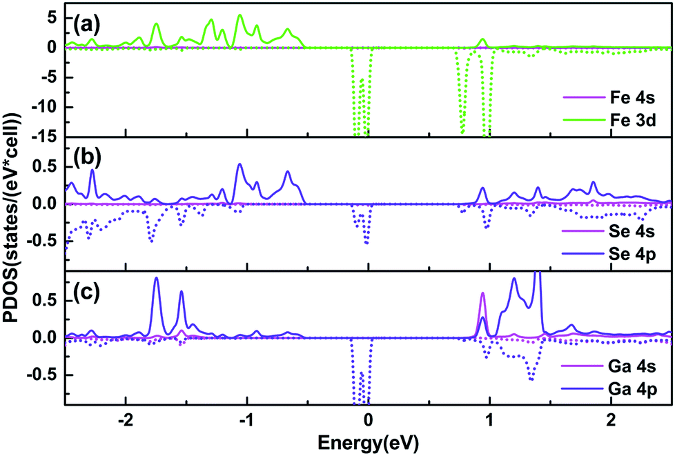 | ||
| Fig. 3 PDOS of (a) the Fe adatom and its nearest neighbour (b) Se and (c) Ga atoms. The solid and dashed lines denote the majority and minority spin states, respectively. | ||
States hybridization effect is further confirmed by the spin-resolved band contributions calculated from the Fe and nearest neighbour Se and Ga atoms, as shown in Fig. 4. In the majority spin channel, the adsorbed Fe atom possesses mainly the top few levels of the valence band, bringing about a redistribution of the coupling electronic states from the three nearest Se atoms. While in the minority spin channel, electronic states of the Fe atom occupy mainly the vicinity of the Fermi energy and the bottom of the conduction band, which arouses a redistribution of the electronic states from the nearest Ga atom. Bader charge analysis suggests that charge transfer occurs from Fe-4s orbital to 3d orbital due to the orbital hybridizations between Fe and the surrounding atoms, leaving about 2 e electrons unpaired and thus generating a magnetic moment of 2.122 μB. The induced magnetic moments of the nearest neighbour Ga atom and Se atoms are −0.004 μB and −0.178 μB, respectively, indicating an antiferromagnetic (AFM) coupling with the Fe atom and producing a total magnetic moment of 1.915 μB in the system, as listed in Table 2. The value of the total magnetic moment is close to that of Fe adsorbed graphene ML (2.13 μB),31 but much lower than that of the Fe doped GaSe ML (5 μB)19 and GaS ML (5 μB).30 Stability of the magnetic moments is verified by the spin polarization energy calculated from the energy difference of the Fe adsorbed GaSe system with and without the consideration of spin polarization. The result shows a 0.02 eV per atom spin polarization energy for the system, which is large enough to keep the stability of the magnetism.
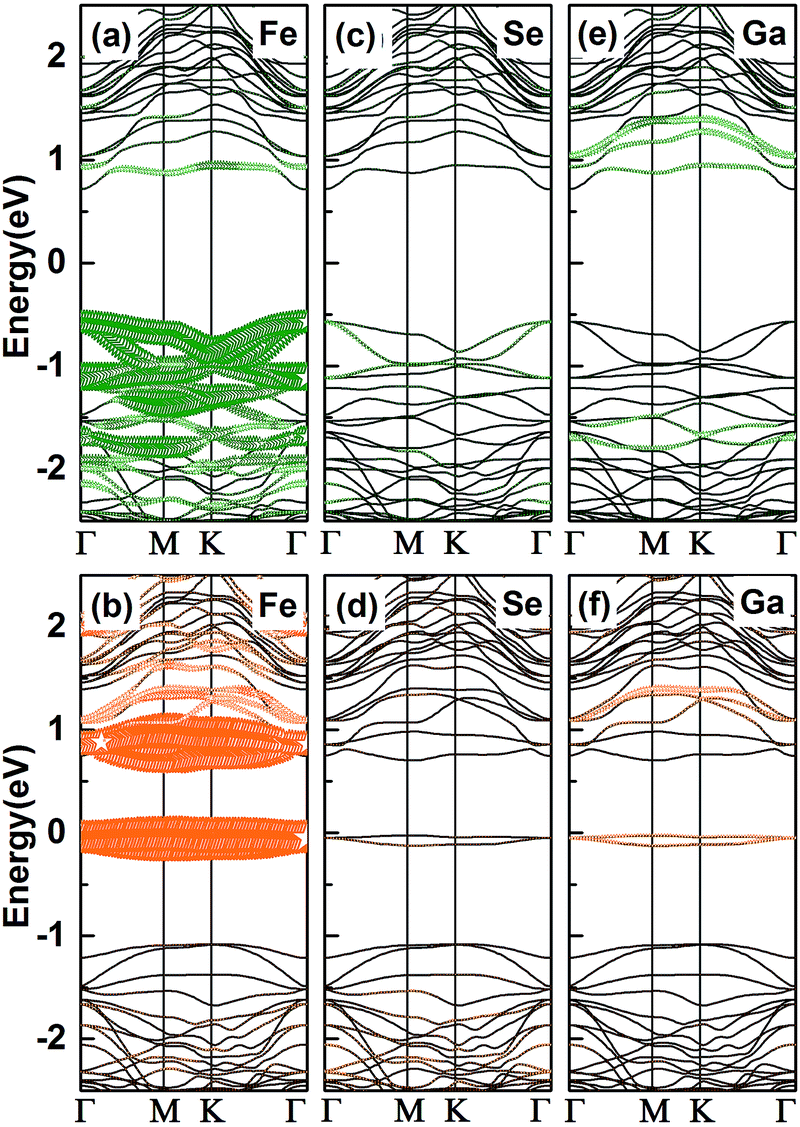 | ||
| Fig. 4 Spin-resolved energy band contributions calculated from (a and b) the Fe adatom and its nearest neighbour (c and d) Se and (e and f) Ga atoms. The top and the bottom half are the majority and minority spin band structures, respectively. | ||
In order to reveal the interaction and the charge redistributions between Fe adatom and underlying GaSe in real space, the deformation charge densities Δρ(r) are calculated via the expression:
 are the charge densities of the Fe/GaSe system and the isolated atom, respectively. Fig. 5 shows the vertical sections of deformation charge densities of pristine and Fe adsorbed GaSe MLs along the (11−20) plane. For the pristine GaSe, negative charge densities are observed at the center of the Ga and Se atoms, which infers the transfer of the valence electrons. On the other hand, positive charge densities trend to accumulate between Ga–Ga and Ga–Se covalent bonds and at the top of Se atoms, which means that adjacent atoms form strong covalent bonds. Such charge distribution accounts for strong intralayer Ga–Ga and Ga–Se covalent bonds and weak interlayer van der Waals' stacking. For Fe adsorbed GaSe ML, the charge densities in the center of Fe adatom is significantly negative, which infers a dramatic transfer of the valence electrons. Compared with the pristine GaSe, the charge densities between Ga and Se atoms near the Fe atom decrease, suggesting a weakened interaction between the nearest Ga and Se atoms after the adsorption of Fe atom. On the other hand, the increasing charge densities are found in the middle of the Fe–Ga and Fe–Se bonds, indicative of strong interactions between Fe–Ga and Fe–Se atoms. Consequently, we can suggest that the strong interaction between the Fe adatom and the GaSe ML is responsible for the real-space charge redistributions, inducing the magnetic moments and polarized spin states in nonmagnetic GaSe ML.
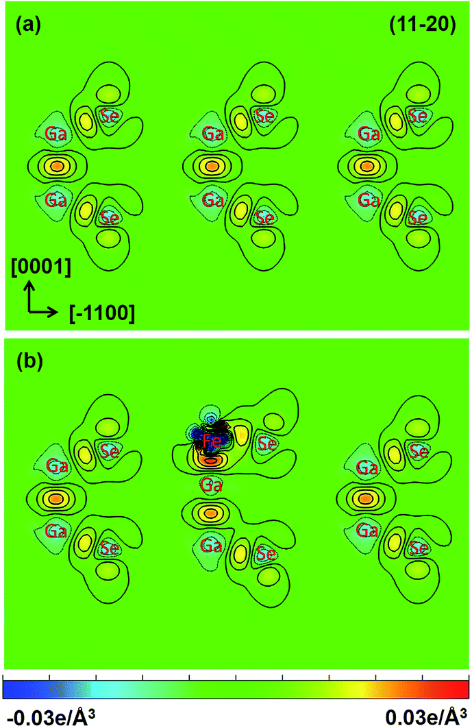 | ||
| Fig. 5 The vertical sections of deformation charge densities of the (11−20) plane of GaSe ML (a) without and (b) with Fe adsorption, containing the Fe–Se and Fe–Ga bonds. The negative and positive contours are respectively shown with blue dashed lines and black solid lines with the contour interval of 0.003 e Å−3. | ||
Spin-resolved partial charge of Fe/GaSe system are further calculated, to study the spatial distribution of the coupled electronic states in the system. Certain energy regions are selected, involving the top of the valence band, the bottom of the conduction band, and the vicinity of the Fermi level, as shown in Fig. 6. The top of the valence band (energy range of about −1.0 to −0.5 eV) is dominated by Fe-3d and Se-4p states in the majority spin channel, while the minority spin channel is empty. Due to an electron transfer from the Fe atom to the nearest Se and Ga atoms, the spin density distributes as a planar triangle shape above the Fe atom, and the induced spin density to Se-4p orbit exhibits a typical bell shape, as shown in Fig. 6(a). The charge densities between Fe and Se atoms are more than that between Fe and Ga atoms, indicating a stronger orbit coupling between the former than the later in the energy range. The bottom of the conduction band (energy range of about +0.5 to +1.0 eV) is composed of Fe-3d, Ga-4p and Ga-4s orbitals including both the majority and minority spin channels. Spatial charge densities in the minority spin channel mostly accumulate around the Fe adatom with a three-folded symmetry. While in the majority spin channel, charge densities present on top of the Fe atom, with the induced spin charge distributing between Fe–Ga bond and on top of the lower Ga atom, as shown in Fig. 6(b). The vicinity of the Fermi level is composed of hybridized Fe-3d, Se-4p, and Ga-4p orbitals in the minority spin channel and without the majority spin channel. Spatial charge density of the Fe atom looks like two reversed triangles, with the corners of the upper one laying towards the three nearest Se atoms, and the lower one showing a strong coupling with the underlying Ga atom. The induced spin charge shows an obvious accumulation between the Fe and Ga atoms, as shown in Fig. 6(c), which indicates a stronger interaction between Fe and Ga atom compared with that between Fe and Se atoms. These results visually display the spatial coupled electronic states of Fe/GaSe system that the induced majority and minority spin states are inclined to distribute on the Se and Ga atoms separately.
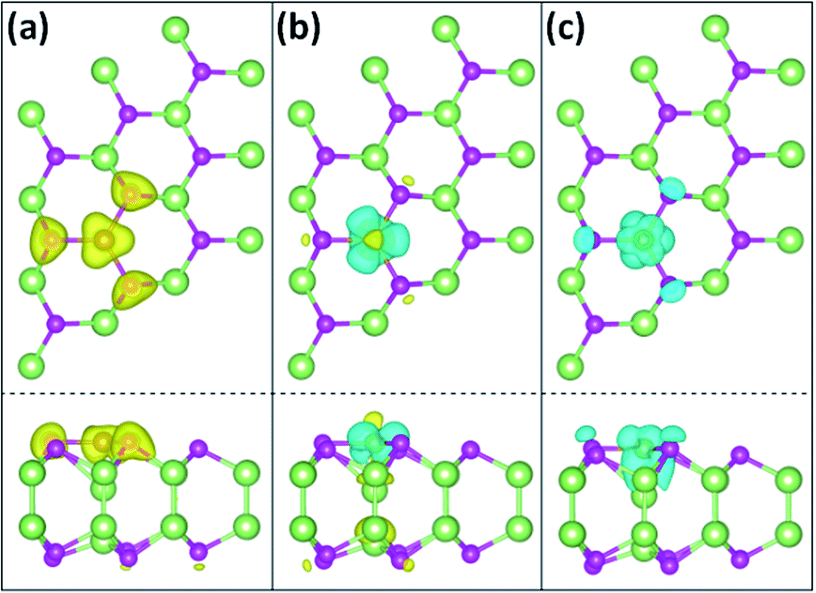 | ||
| Fig. 6 Spin charge of Fe/GaSe system in the energy range (a) −1.0 to −0.5 eV, (b) +0.5 to +1.0 eV, and (c) −0.5 to 0.0 eV. The charge densities of majority and minority spin channels are denoted by yellow and blue colours, respectively. | ||
4 Conclusions
In conclusion, the structural and electronic properties of Fe adsorbed GaSe ML are investigated systematically by using the first-principles DFT calculations. Adsorption energy results infer a most favourite site on the top of Ga atom. Spin-resolved band structures and the TDOS suggest a strong orbit coupling between Fe and vicinal Ga and Se atoms, which induces n-type conduction interface states near the Fermi level, and results in a half-metallicity with 100% spin polarization in the system. PDOS and energy band contributions are also calculated to analyze the orbit coupling effect of different atoms. The CBM is dominated by hybridized Fe-3d, Ga-4p and Ga-4s orbitals in both the majority and minority spin channels, the top of the valence band is dominated by Fe-3d and Se-4p states only in the majority spin channel, and the vicinity of the Fermi level is distributed with hybridized Fe-3d, Se-4p, and Ga-4p orbitals only in the minority spin channel. Attributed to the transfer of Fe-3d electrons, the magnetic moments of −0.004 μB and −0.178 μB are induced for the nearest neighbour Ga and Se atoms, respectively, showing an AFM coupling with the adsorbed Fe atom. Deformation charge densities as well as the partial spin charge distribution are further analyzed, which is responsible for the induced magnetic moments and spin polarization in nonmagnetic GaSe ML. The present work reveals the spin electronic properties of the typical ferromagnetic/GaSe adsorption system, which may provide some references for the design and construction of 2D spin nanostructures.Acknowledgements
The work was supported by the National Natural Science Foundations of China (No. 61674124, 11304257, 11604275, and 61227009), the National Key Research and Development Program of China (No. 2016YFB0400801), Natural Science Foundation of Fujian Province of China (No. 2014J01026, 2016J01037, and 2015J01028), and Fundamental Research Funds for the Central Universities (No. 20720160122, 20720150033, and 20720160044).References
- K. S. Novoselov, A. K. Geim, S. V. Morozov, D. Jiang, Y. Zhang, S. V. Dubonos, I. V. Grigorieva and A. A. Firsov, Science, 2004, 306, 666 CrossRef CAS PubMed.
- Y. B. Zhang, Y. W. Tan, H. L. Stormer and P. Kim, Nature, 2005, 438, 201 CrossRef CAS PubMed.
- X. Du, I. Skachko, A. Barker and E. Y. Andrei, Nat. Nanotechnol., 2008, 3, 491 CrossRef CAS PubMed.
- S. Y. Zhou, G. H. Gweon, A. V. Fedorov, P. N. First, W. A. De Heer, D. H. Lee, F. Guinea, A. H. C. Neto and A. Lanzara, Nat. Mater., 2007, 6, 770 CrossRef CAS PubMed.
- X. L. Li, X. R. Wang, L. Zhang, S. W. Lee and H. J. Dai, Science, 2008, 319, 1229 CrossRef CAS PubMed.
- L. Song, L. J. Ci, H. Lu, P. B. Sorokin, C. H. Jin, A. G. Kvashnin, D. G. Kvashnin, J. Lou, B. I. Yakobson and P. M. Ajayan, Nano Lett., 2010, 10, 3209 CrossRef CAS PubMed.
- P. Vogt, P. D. Padova, C. Quaresima, J. Avila, E. Frantzeskakis, M. C. Asensio, A. Resta, B. Ealet and G. L. Lay, Phys. Rev. Lett., 2012, 108, 155501 CrossRef PubMed.
- E. Bianco, S. Butler, S. S. Jiang, O. D. Restrepo, W. Windl and J. E. Goldberger, ACS Nano, 2013, 7, 4414 CrossRef CAS PubMed.
- S. F. Wu, S. Buckley, J. R. Schaibley, L. F. Feng, J. Q. Yan, D. G. Mandrus, F. Hatami, W. Yao, J. Vuckovic, A. Majumdar and X. D. Xu, Nature, 2015, 520, 69 CrossRef CAS PubMed.
- D. J. Late, B. Liu, J. J. Luo, A. M. Yan, H. S. S. R. Matte, M. Grayson, C. N. R. Rao and V. P. Dravid, Adv. Mater., 2012, 24, 3549 CrossRef CAS PubMed.
- P. Hu, L. Wang, M. Yoon, J. Zhang, W. Feng, X. Wang, Z. Wen, J. C. Idrobo, Y. Miyamoto, D. B. Geohegan and K. Xiao, Nano Lett., 2013, 13, 1649 CrossRef CAS PubMed.
- D. J. Late, B. Liu, H. S. S. R. Matte, C. N. R. Rao and V. P. Dravid, Adv. Funct. Mater., 2012, 22, 1894 CrossRef CAS.
- P. A. Hu, Z. Z. Wen, L. F. Wang, P. H. Tan and K. Xiao, ACS Nano, 2012, 6, 5988 CrossRef CAS PubMed.
- E. M. Gamarts, E. L. Ivchenko, M. I. Karaman, V. P. Mushinski, G. E. Pikus, B. S. Razbirin and A. N. Starukhin, J. Exp. Theor. Phys., 1977, 46, 590 Search PubMed.
- E. L. Ivchenko, G. E. Pikus, B. S. Razbirin and A. I. Starukhin, J. Exp. Theor. Phys., 1977, 45, 1172 Search PubMed.
- W. Wei, Y. Dai, C. W. Liu, Y. D. Ma and B. B. Huang, J. Mater. Chem. C, 2015, 3, 11548 RSC.
- T. Cao, Z. L. Li and S. G. Louie, Phys. Rev. Lett., 2015, 114, 236602 CrossRef PubMed.
- Y. T. Peng, C. X. Xia, H. Zhang, T. X. Wang, S. Y. Wei and J. Jia, Phys. Chem. Chem. Phys., 2014, 16, 18799 RSC.
- L. Ao, H. Y. Xiao, X. Xiang, S. Li, K. Z. Liu, H. Huang and X. T. Zu, Phys. Chem. Chem. Phys., 2015, 17, 10737 RSC.
- W. G. Wang, M. Li, S. Hageman and C. L. Chien, Nat. Mater., 2012, 11, 64 CrossRef CAS PubMed.
- S. Ikeda, K. Miura, H. Yamamoto, K. Mizunuma, H. D. Gan, M. Endo, S. Kanai, J. Hayakawa, F. Matsukura and H. Ohno, Nat. Mater., 2010, 9, 721 CrossRef CAS PubMed.
- T. Maruyama, Y. Shiota, T. Nozaki, K. Ohta, N. Toda, M. Mizuguchi, A. A. Tulapurkar, T. Shinjo, M. Shiraishi, S. Mizukami, Y. Ando and Y. Suzuki, Nat. Nanotechnol., 2009, 4, 158 CrossRef CAS PubMed.
- G. Kresse and J. Hafner, Phys. Rev. B: Condens. Matter Mater. Phys., 1994, 49, 14251 CrossRef CAS.
- G. Kresse and J. Furthmüller, Phys. Rev. B: Condens. Matter Mater. Phys., 1996, 54, 11169 CrossRef CAS.
- G. Kresse and J. Joubert, Phys. Rev. B: Condens. Matter Mater. Phys., 1999, 59, 1758 CrossRef CAS.
- J. P. Perdew, K. Burke and M. Ernzerhof, Phys. Rev. Lett., 1996, 77, 3865 CrossRef CAS PubMed.
- Y. D. Ma, Y. Dai, M. Guo, L. Yu and B. B. Huang, Phys. Chem. Chem. Phys., 2013, 15, 7098 RSC.
- L. Huang, Z. H. Chen and J. B. Li, RSC Adv., 2015, 5, 5788 RSC.
- J. Zhou, RSC Adv., 2015, 5, 94679 RSC.
- H. Chen, Y. Li, L. Huang and J. B. Li, J. Phys. Chem. C, 2015, 119, 29148 CAS.
- C. Cao, M. Wu, J. Z. Jiang and H. P. Cheng, Phys. Rev. B: Condens. Matter Mater. Phys., 2010, 81, 205424 CrossRef.
| This journal is © The Royal Society of Chemistry 2017 |