DOI:
10.1039/C6RA26776A
(Paper)
RSC Adv., 2017,
7, 4278-4284
Characterization and optimization of the growth conditions of a novel Cs2TeW3O12 piezoelectric crystal†
Received
14th November 2016
, Accepted 27th December 2016
First published on 16th January 2017
Abstract
In this study, Cs2TeW3O12 (CTW) single crystals were grown successfully through a top-seeded solution growth (TSSG) method using TeO2 as a self-flux. We identified a complete set of growth process parameters suitable for facilitating the growth of a high-quality CTW crystal. The results indicate that, in the same thermal field and with an appropriate flux ratio, a smaller cooling rate of the melt facilitates the smooth growth of high-quality CTW single crystals. The melt-viscosity versus temperature curves for different flux ratios were measured, and their effects on the crystal quality were discussed. In addition, the morphology of the crystal can be controlled by adjusting the rotation speed and the orientation of the seed. To investigate piezoelectric performance, complete sets of dielectric, elastic, and piezoelectric coefficients of CTW crystals were measured using both resonance and impedance analysis. The piezoelectric coefficients d33 and d15 reached 19.1 pC N−1 and 25.9 pC N−1, respectively. The electromechanical coupling coefficient, k33, was 37.7%, slightly higher than that of Cs2TeMo3O12 (CTM). Furthermore, the extent of dipole moment and polyhedron distortion of the CTW crystal were analysed in detail, and the relationship between the crystal structure and the piezoelectric properties was also discussed.
Introduction
Because piezoelectric crystals enable transfer between mechanical energy and electrical energy, a variety of piezoelectric devices, such as ultrasonic transducers, filters, and piezoelectric transformers, have become available for both military and civil purposes. These include national defence, aerospace, communications, and healthcare.1–3 As a result, piezoelectric crystals have become an indispensable functional material for modern electronic technology. In order to meet the demand of many applications, the number of discovered piezoelectric crystal types increased rapidly and now exceeds one thousand. At present, it is of great urgency and practical significance to find lead-free piezoelectric materials with a large piezoelectric coefficient and low dielectric loss.4–11 Recently, the design and synthesis of non-centrosymmetric inorganic oxides using the second-order Jahn–Teller effects (SOJT) has triggered widespread interest by researchers since these materials show excellent piezoelectric, pyroelectric, ferroelectric and nonlinear properties. A category of oxides, which contain distorted octahedrally-coordinated d0 transition metals (Mn+ = Mo6+, W6+, V5+, Ti4+, etc.) and a lone-pair cation (Am+ = I5+, Te4+, Se4+, Sb3+, etc.), have been synthesized and demonstrated to be potential NLO materials.12,13 Due to the SOJT, the former will cause distortion toward the direction of a face, an edge or a vertex of the octahedron. With regard to the latter, the lone electron pair causes the coordinating oxygen atoms surrounding cations to move in the opposite direction. This produces a non-centrosymmetric unit, which eventually, macroscopically endows the material with a series of piezoelectric, pyroelectric, and nonlinear properties. Based on this design concept, a series of materials with excellent piezoelectric properties such as β-BaTeMo2O9 (β-BTM), CTM and Na2TeW2O9 (NTW) have been synthesized.14–16 Bulk single crystal materials need to be included in the study of relevant physical properties. Therefore, in recent years, our group devoted much time to growing large-sized single crystals, and we obtained good results. Among these results, CTM crystals are among the most representative multifunctional materials. CTM crystals crystallize in the polar hexagonal space group P63. Under the influence of the SOJT, the TeO3 and MoO6 polyhedra are distorted. All of the TeO3 polyhedra have a consistent direction of the distortion, which generates a very large net dipole moment along the crystallographic c-axis. Previous research revealed that its longitudinal piezoelectric strain constant, d33, was 20.3 pC N−1, 8.8 times that of SiO2, and similar to that of LiNbO3. Because of its higher electromechanical coupling coefficient and less significant temperature dependence, the CTM crystal is a promising candidate to be used in piezoelectric devices.17 However, in our experimental crystal growth process, we found that the flux of CTM crystal exhibits a high viscosity value, which can lead to cracking and unwanted inclusions in the crystal. The CTW crystal as a tungstate material is isostructural to the CTM crystal. Because of its better thermal stability and ability to grow readily into high-quality single crystals, CTW crystals can be useful piezoelectric single crystals with broad application prospects.18
In this article, the effects of relevant growth process parameters on the crystal quality and morphology, were discussed and explored. In addition, the complete sets of room-temperature piezoelectric coefficients of CTW crystals were measured. The relationship between the crystal structure and its piezoelectric properties was also discussed.
Experimental section
Flux exploration for CTW crystal growth
Since CTW crystals are incongruent melting compounds, only the flux method can be used for crystal growth. Whether the flux method can be successful mainly depends on finding a suitable flux agent. The complex chemical reactions that can occur between flux and solute result in various phases and directly affect the growth of the primary crystal phase. Currently, there is no detailed flux selection theory to follow, so the selection is still mainly based on experience and experimentation. In order to avoid the artificial introduction of external impurity ions, we give priority to using self-flux such as TeO2, WO3, and TeO2–WO3 for crystal growth. After intensive experimental exploration, we have identified the approximate suitable flux ratio for CTW crystal growth and reported it in a previously published paper.18
Melt-viscosity measurement
Crystal growth is, in essence, a phase transition process, which is accompanied by the movement of atoms, changes in the structure of the cluster, and restructuring of coordinating atoms, which are all related to the transport properties of the melt. Viscosity is an important physical quantity reflecting the momentum transport inside the reaction melt. The Orton RSV-1600-type rotary high-temperature viscometer (Orton, USA) was used to measure the viscosity. The viscometer has a measurement range from 50 cp to 4 × 10⁷ cp, a temperature variation of less than ±0.1 K, and viscosity error of ±1%. The raw materials were weighed according to the required ratio, mixed uniformly, and poured into a special platinum crucible to measure the viscosity. The center of the platinum crucible was adjusted to be coaxial with the rotation axis of the viscometer. In this experiment, the sample was heated to 700 °C at a heating rate of 10 °C min−1 and kept for 10 hours to ensure complete melting. Then, the viscosity versus temperature curve was measured at a cooling rate of 1 °C min−1.
Thermal field during crystal growth
In both the melt method and the high-temperature solution method, during the crystal growth process, the thermal field distribution has a crucial effect on the crystal growth behavior. The temperature depends on the position inside the furnace chamber. In other words, at any given time, each position in the furnace has a certain temperature, while the temperatures at different points may be different; such a spatial temperature distribution is referred to as thermal field. The uneven thermal field can cause a variety of internal macroscopic defects in the crystal such as growth stripes, inclusions, which affect the optical quality of the growing crystal. The thermal field distribution inside the furnace is often described by two gradients, the axial thermal gradient, and the horizontal thermal gradient. The horizontal thermal gradient is preferably centro-symmetric, which can be achieved by adjusting both the crucible center and furnace center to coincide. The axial thermal gradient distribution should be suitable: a wider temperature gradient distribution can accelerate crystal growth but it is prone to generate inclusions and other defects or impurities in the crystal. A narrow thermal gradient distribution, on the other hand, encourages the growth of a high-quality crystal but it can reduce the growth rate. Therefore, finding the appropriate thermal field is one of the keys for growing high-quality crystals. After many years of growing crystals, our group found that the optimum thermal gradient should be relatively small for crystal growth using the flux method because this ensures a greater constant-temperature region to exist in the position where we place the crucible. Since the growth temperature range in our experiments was around 600–700 °C, we mainly tested the thermal gradient in this range. An empty platinum crucible was placed in the center position at the bottom of the vertical furnace. A quartz tube with a diameter of 22 mm was wrapped by layers of insulation cotton, and it vertically covers the platinum crucible. The top end of the quartz tube was aligned with the furnace mouth, and the gap between furnace and quartz tube was filled tightly with insulation cotton. This ensures that the platinum crucible was placed inside a relatively stable and insulated environment. After that, a Pt–Rh/Pt thermocouple was inserted into the quartz tube and then slowly moved into the furnace to record the temperature at different positions in the furnace chamber.
Crystal growth
During the process of crystal growth, even under the same thermal field, there are many factors affecting the crystal morphology and quality, such as the viscosity and the cooling rate of the melt, the rotation speed and the orientation of the seed. In order to explore the appropriate growth process, we studied the crystal growth in different growth conditions. The growth instrument was a homemade vertical furnace, heated by resistance wire. The temperature-control equipment was an FP21 programmable automatic temperature controller (SHIMADEN, Japan) that can ensure temperature accuracy within 0.1% for crystal growth. A Pt–Rh/Pt thermocouple was used to measure temperature. Cs2CO3 (Alfa Aesar, 99.9%), TeO2 (Alfa Aesar, 99.99%), and WO3 (Alfa Aesar, 99.8%) were mixed uniformly, compacted, and placed into the platinum crucible. The crucible was placed in the center of the heating furnace. The temperature was slowly raised from room temperature to 750 °C in order to achieve complete melting of the raw materials, and the temperature was kept constant for 24 hours in order to ensure a sufficient reaction between the raw materials. After obtaining a uniform solution with the stirring blade, we used the TSSG method to determine the saturation temperature of the melt. For example, at a certain temperature, the seed crystal was immersed in the melt and the state of seed observed after 10–12 hours. If the seed melted, it indicated that the melt was an unsaturated melt at that temperature. If the seed grew, it indicated that the melt was a supersaturated melt at that temperature. If the state variation of the seed was not significant, the saturation temperature had been reached. An oriented seed was attached at the bottom of the quartz rod with a platinum wire. The quartz rod was fixed above the vertical furnace such that it can slowly slide into the furnace. The seed was preheated for 5 minutes at about 2 cm above the surface of the melt and then immersed in the melt with 5 °C higher than the saturation temperature. Then 30 minutes are needed to melt the seed slightly, which can reduce the impurities or avoid introducing self-defects of the seed into the growing crystal. Then the seed was rapidly cooled to the saturation temperature, and the crystal growth process was initiated according to a defined temperature program. After the crystal growth process had finished, the crystal was lifted to a position about 1 cm above the surface of melt, cooled to 100 °C at a cooling rate of 10 °C h−1, and then naturally cooled to room temperature when the power was turned off.
Dielectric properties
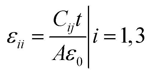
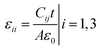
The dielectric constant of the crystal is an important macroscopic quantity that can comprehensively reflect the polarization behavior of the dielectric. The CTW, a hexagonal crystal, has only two independent dielectric constants, ε11 and ε33, which can be obtained from the capacitances of the X and Z square piece, respectively. The capacitances can be measured at 1 kHz at room temperature with an Agilent 4294A type LCR. The dielectric constant can be calculated as follows:| |
 | (1) |
where A is the area of the crystal plate, t is the thickness of crystal plate, C is the capacitance, ε0 is the vacuum dielectric constant.
Elastic and piezoelectric properties
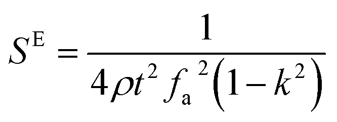
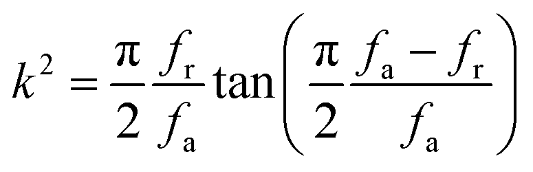
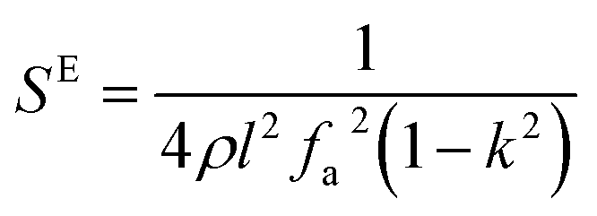
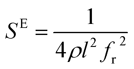
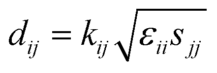
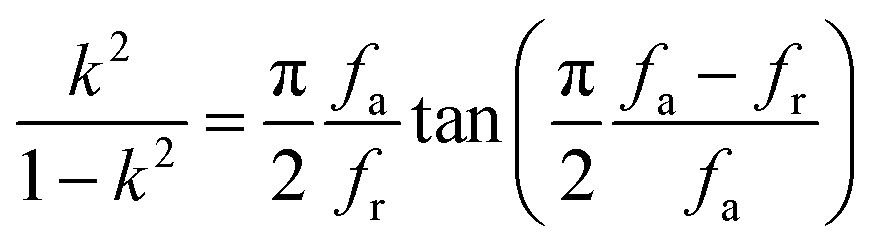
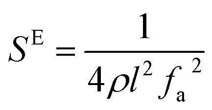
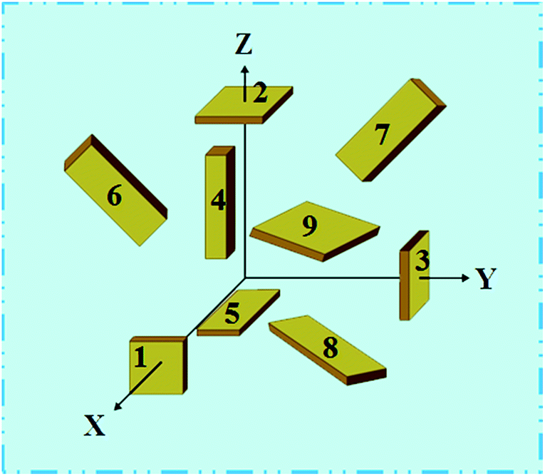
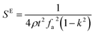
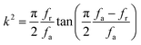
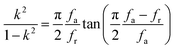
The elastic and piezoelectric coefficients were measured using the resonant technique and impedance analysis. For the CTW crystal, the correspondence between the piezoelectric coordinate system and the crystallographic coordinate system is: X∥a, Z∥c, and the X, Y, Z-axis fit the right-hand screw rule. The positive direction of the Z-axis and d33 was determined using a quasi-static piezoelectric d33 meter (model ZJ-2, Institute of Acoustic Academia Sinica, Beijing, China). There are four independent piezoelectric constants and five independent elastic constants of the CTW crystal, which can be determined using the nine samples with different orientations as shown in Fig. 1. These samples can be divided into two categories: noncircumgyrate samples (1–5 specimens in the figure) and circumgyrate samples (6–9 specimens in the figure). According to the IEEE standard for symbols of the piezoelectric crystals, the first letter represents the direction of the thickness and the second letter represents the direction of the length. Other letters represent the rotation edge directions of the wafer, which are t, l, w, respectively, representing the rotation axis along thickness, length, and width directions. In Fig. 1, the dimensions of the square piece are 4 × 4 × 1 mm3, the size of the rectangular bars is 5 × 2 × 1 mm3, and the size of a Z rod is 6 × 3 × 3 mm3, wherein all the rotation angles of the circumgyrate sample are 45°. The dimensional errors along each direction of samples are less than 3%. All samples were coated with silver electrodes in the direction of the applied electric field. Table 1 lists the specimen orientations and shapes, the vibration modes, and the corresponding elastic and piezoelectric coefficients which were measured. Using the surface-shear vibration mode of the Y square plate, the s55 and k15 were determined through eqn (2) and (3). The electromechanical coupling coefficient, k33 can also be obtained through eqn (3). Using the longitudinal length extensional vibration mode excited by the piezoelectric constant d33, s33 can be determined through eqn (4). Applying an electric field in the thickness direction of samples 5, the elastic coefficients s11 and piezoelectric coefficients d31 were obtained using eqn (5) and (6). With the help of the circumgyrate samples, i.e. samples 6, 7, 8, and 9, four elastic coefficients (s12, s13, s44, and s66), and two piezoelectric coefficients (d14 and d15) were determined using eqn (6)–(14). After obtaining all piezoelectric coefficients and elastic coefficients, the elastic stiffness coefficient cij can be obtained using eqn (15). By measuring the capacitances, resonance frequencies, and anti-resonance frequencies of different samples, we get a complete set of dielectric, elastic, and piezoelectric coefficients for the CTW crystal.| |
 | (2) |
| |
 | (3) |
| |
 | (4) |
| |
 | (5) |
| |
 | (6) |
| |
 | (7) |
| |
 | (8) |
| | |
s′22(XYt)45° = (s22 + s33 + 2s13 + s44)/4
| (9) |
| | |
s′11(ZXt)45° = (s11 + s22 + 2s12 + s66)/4
| (10) |
| | |
s′55(YZw)45° = (s44 + s66)/2
| (11) |
| | |
d′11(XZw)45° = −0.354(d33 + d31 + d15)
| (12) |
| | |
d′13(XZw)45° = −0.354(d33 + d31 − d15)
| (13) |
| | |
d′12(XYt)45° = 0.5d14
| (14) |
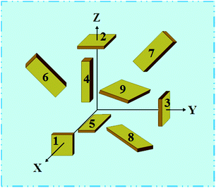 |
| | Fig. 1 Schematic diagram of the specimens for measuring the dielectric, elastic, and piezoelectric constants. | |
Table 1 Summary of the elastic and piezoelectric constants for different specimens and vibration modesa
| No. |
Sample |
Modes |
Constants |
| LLE: longitudinal length extensional vibration mode; TLE: transverse length extensional vibration mode; TS: thickness shear vibration mode. |
| 1 |
X square plate |
|
ε11 |
| 2 |
Z square plate |
|
ε33 |
| 3 |
Y square plate |
|
s55, k15 |
| 4 |
Z rod |
LLE |
d33, s33, k33 |
| 5 |
ZX bar |
LLE, TS |
d31, s11, k31 |
| 6 |
(ZXw)45° bar |
TLE |
d15 |
| 7 |
(XYt)45° bar |
LLE, TS |
d14, (2s13 + s44) |
| 8 |
(ZXt)45° bar |
TLE |
(2s12 + s66) |
| 9 |
(YZw)45° square plate |
TLE |
s66 |
Results and discussion
Growth conditions effect on crystal quality: cooling rate and viscosity of the melt
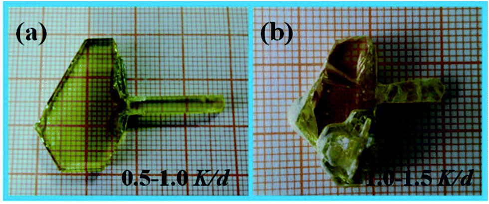
By comparing with the crystals labeled a and b in Fig. 2, we find that the cooling rate of the melt has a significant impact on the crystal quality. When the cooling rate is higher than 1 °C per day, the as grown crystal is only partially transparent and the amount of inclusions increased significantly. In addition, the higher precipitation rate of solute during the crystal growth process causes the formation of a large number of impure phases. The impure phases are adsorbed on the crystal surface and strongly affect the crystal quality. When the cooling rate is controlled within the range of 0.5–1.0 °C per day, the optical quality of the crystal significantly improved, and no impure phase is observed. Therefore, a low cooling rate of the melt is more suitable to grow a CTW crystal.
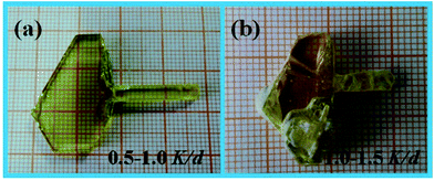 |
| | Fig. 2 Photographs of the CTW crystals grown under different cooling rates. | |
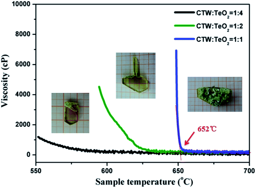
The viscosity of different flux varied largely so that the crystal quality can be strongly diversified.19 After determining the optimized cooling rate of the melt, we explored the impact of melt-viscosity on the crystal quality. The experimental viscosity curves as a function of temperature, for different flux ratios, are presented in Fig. 3. In addition, single crystal growth was carried out with three flux ratios in order to confirm the effect of melt-viscosity on the actual crystal growth. A comparison between these three crystals which are shown in Fig. 3 indicates that even for the same cooling rate, the crystals grown with different viscosity have clearly different quality. The lowest viscosity of the melt was obtained when the ratio between CTW and TeO2 was 1![[thin space (1/6-em)]](https://www.rsc.org/images/entities/char_2009.gif) :4, resulting in a better optical quality but smaller crystal dimension. This happened because an insufficient solute concentration results in a low amount of precipitated ‘growth unit’ per unit time. As the ratio of the CTW and TeO2 increased to 1:1, the viscosity of the melt clearly increased at about 652 °C. This indicates that the CTW crystals began to precipitate. In the same conditions, the precipitated ‘growth unit’ per unit time increased, however more impure phases grow. When the ratio between CTW and TeO2 was 1:2, the measured viscosity value was moderate, the crystal quality was significantly improved. This indicates that neither too high nor too low solute concentrations are suitable for CTW crystal growth. A more detailed exploration of the relevant mechanism that affects melt-viscosity during actual crystal growth will be reported in a separate paper very soon.
:4, resulting in a better optical quality but smaller crystal dimension. This happened because an insufficient solute concentration results in a low amount of precipitated ‘growth unit’ per unit time. As the ratio of the CTW and TeO2 increased to 1:1, the viscosity of the melt clearly increased at about 652 °C. This indicates that the CTW crystals began to precipitate. In the same conditions, the precipitated ‘growth unit’ per unit time increased, however more impure phases grow. When the ratio between CTW and TeO2 was 1:2, the measured viscosity value was moderate, the crystal quality was significantly improved. This indicates that neither too high nor too low solute concentrations are suitable for CTW crystal growth. A more detailed exploration of the relevant mechanism that affects melt-viscosity during actual crystal growth will be reported in a separate paper very soon.
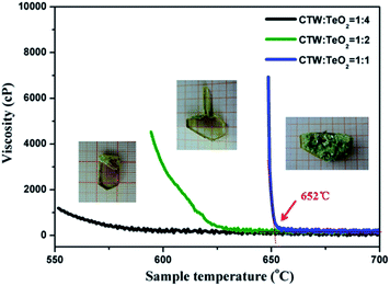 |
| | Fig. 3 Viscosity versus temperature curves for different flux ratios and the as grown crystal growth with the corresponding flux ratios. | |
Growth conditions effect on crystal morphology: rotation speed and orientation of the seed
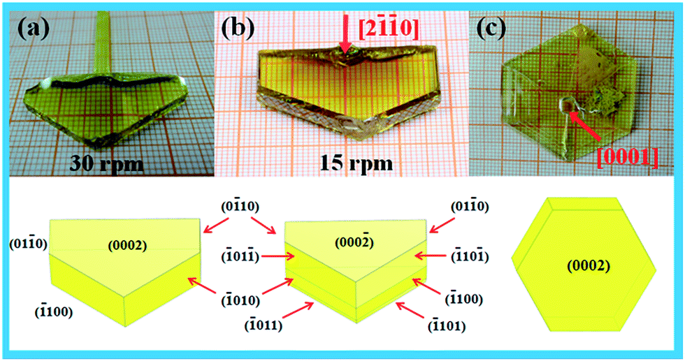
Fig. 4 shows the as-grown CTW crystals with different rotation speeds and different seed orientations and the theoretical morphology with indexed (hkl) facets according to the Bravais–Friedel and Donnay–Harker (BFDH) method.20 As can be seen from Fig. 4(a), the rotation speed of seed was 30 rpm, and the grown crystal hereafter called crystal a has a size of 32 × 16 × 5 mm3 and exhibits (01![[1 with combining macron]](https://www.rsc.org/images/entities/char_0031_0304.gif) 0), (100), (010), (010), and (0002) facets. The crystal grown with a rotation speed of 15 rpm hereafter called crystal b has a size of 36 × 25 × 6 mm3 (Fig. 4(b)). However, in addition to all crystal facets of crystal a, crystal b reveals some small facets of (101), (10), (011), and (01) which are not observed in crystal a. Although the microscopic mechanism for crystal growth remains unclear, introducing the concept of a ‘boundary layer theory’ can help us better understand this phenomenon.21 The ‘boundary layer’ is a thin layer between melt and crystal interface, in which the concentration of the ‘growth unit’ dramatically changes. The transport of the ‘growth unit’ in the thin layer was achieved by convection–diffusion process. The thinner the ‘boundary layer’, the lower the transport speed of the ‘growth unit’, and the transport becomes faster for a thicker ‘boundary layer’. However, the thickness of the ‘boundary layer’ has a very close relationship with the rotation speed of the seed. The low seed rotation speed forms a thicker ‘boundary layer’ resulting in a lower transport speed of the ‘growth unit’. Therefore, for low seed rotation speed, the thickness of the boundary layer is the dominant factor while the effect of anisotropy is smaller. As a consequence, the growth rates of facets are similar and the crystal facet with higher growth rate is first revealed regardless of the anisotropic effect. As the seed rotation speed increases, the boundary layer becomes thinner. In this condition, the crystal growth was mainly controlled via the kinetic effect. Therefore, the effect of anisotropy on the crystal facet growth becomes visible.19 This explains why the small crystal facets with high growth rates disappear, and the crystal facets with low growth rates become visible. Using this theory, we can explain why crystal b had a more revealed facets than crystal a. This also gives us the hint that we can control the morphology of the as grown crystal by adjusting the rotation speed of the seed.
0), (100), (010), (010), and (0002) facets. The crystal grown with a rotation speed of 15 rpm hereafter called crystal b has a size of 36 × 25 × 6 mm3 (Fig. 4(b)). However, in addition to all crystal facets of crystal a, crystal b reveals some small facets of (101), (10), (011), and (01) which are not observed in crystal a. Although the microscopic mechanism for crystal growth remains unclear, introducing the concept of a ‘boundary layer theory’ can help us better understand this phenomenon.21 The ‘boundary layer’ is a thin layer between melt and crystal interface, in which the concentration of the ‘growth unit’ dramatically changes. The transport of the ‘growth unit’ in the thin layer was achieved by convection–diffusion process. The thinner the ‘boundary layer’, the lower the transport speed of the ‘growth unit’, and the transport becomes faster for a thicker ‘boundary layer’. However, the thickness of the ‘boundary layer’ has a very close relationship with the rotation speed of the seed. The low seed rotation speed forms a thicker ‘boundary layer’ resulting in a lower transport speed of the ‘growth unit’. Therefore, for low seed rotation speed, the thickness of the boundary layer is the dominant factor while the effect of anisotropy is smaller. As a consequence, the growth rates of facets are similar and the crystal facet with higher growth rate is first revealed regardless of the anisotropic effect. As the seed rotation speed increases, the boundary layer becomes thinner. In this condition, the crystal growth was mainly controlled via the kinetic effect. Therefore, the effect of anisotropy on the crystal facet growth becomes visible.19 This explains why the small crystal facets with high growth rates disappear, and the crystal facets with low growth rates become visible. Using this theory, we can explain why crystal b had a more revealed facets than crystal a. This also gives us the hint that we can control the morphology of the as grown crystal by adjusting the rotation speed of the seed.
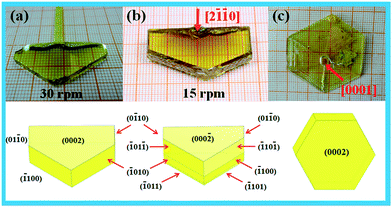 |
| | Fig. 4 Photographs of the CTW single crystal grown under different rotation speeds and with different seed orientations. | |
The orientation of the seed is also an important factor that determines the morphology of a crystal. The experiment method is the same as above. The crystal was cut into small rectangular seeds, and the seeds were immersed into a melt along the [20] and [0001] orientations to grow the crystal. As can be seen from Fig. 4(b) and (c), the morphologies of the as-grown crystals with different seed orientations vary significantly. The crystal growing along the [0001] exhibits a perfect hexagonal symmetry, and its morphology resembles a hexagon; however, the crystal growing along the [20] orientation only shows half of the hexagonal morphology. The crystal morphologies of these two crystals with different seed orientations are both in agreement with the theoretical morphologies. For the crystal with [20] orientation seed, we can determine the corresponding facets such as (010), (100), (101), (10), and (0002). However, for the crystal with the [0001] seed orientation, we can only determine the two opposite facets, i.e. the (0002) and the (000![[2 with combining macron]](https://www.rsc.org/images/entities/char_0032_0304.gif) ) facets, while other facets are too small to be determined. In addition, six uniformly distributed growth ridges can be observed on the crystal grown along the [0001] orientation, which also confirm the presence of a 6-fold axis along the c-axis of the CTW crystal. However, unfortunately, the crystal growing along the [0001] orientation is very thin (around 1 mm) and the crystal quality is poorer, which makes it prone to form inclusions. Moreover, the crystal growing along the [20] orientation is of higher quality and the thickness increased significantly as well. As widely known, the morphology of crystals is the refection of their internal structure, so the crystal growth behavior observed from morphology was inevitably restricted by its internal structure. We speculate that the flaky morphology may result from the layered crystal structure. More precisely, the crystal has a two-dimensional layered structure perpendicular to the c-axis. Every layer consists of wave-connected WO6 octahedra, and TeO3 polyhedra covering the same side of the W–O layer. Cs+ cations fill the gap between layers to achieve a charge balance (Fig. S1, ESI†). The distance between these layers is so large (3.25 Å) that only weaker interaction exists between layers, which indicates that the growth in the chain direction is easier than the growth parallel to the layer direction. This determines the CTW crystal's flaky morphology as it grows along the [0001] orientation, making the (0002) facet much larger than all other facets.
) facets, while other facets are too small to be determined. In addition, six uniformly distributed growth ridges can be observed on the crystal grown along the [0001] orientation, which also confirm the presence of a 6-fold axis along the c-axis of the CTW crystal. However, unfortunately, the crystal growing along the [0001] orientation is very thin (around 1 mm) and the crystal quality is poorer, which makes it prone to form inclusions. Moreover, the crystal growing along the [20] orientation is of higher quality and the thickness increased significantly as well. As widely known, the morphology of crystals is the refection of their internal structure, so the crystal growth behavior observed from morphology was inevitably restricted by its internal structure. We speculate that the flaky morphology may result from the layered crystal structure. More precisely, the crystal has a two-dimensional layered structure perpendicular to the c-axis. Every layer consists of wave-connected WO6 octahedra, and TeO3 polyhedra covering the same side of the W–O layer. Cs+ cations fill the gap between layers to achieve a charge balance (Fig. S1, ESI†). The distance between these layers is so large (3.25 Å) that only weaker interaction exists between layers, which indicates that the growth in the chain direction is easier than the growth parallel to the layer direction. This determines the CTW crystal's flaky morphology as it grows along the [0001] orientation, making the (0002) facet much larger than all other facets.
Elastic and piezoelectric properties
Table 2 lists the dielectric, elastic and piezoelectric coefficients of CTW, CTM, LiNbO3 and SiO2 crystals at room temperature.17,22,23 All the coefficients were measured several times, and the average values are reported. Compared with LiNbO3 and SiO2 crystals, CTW crystals exhibit a better piezoelectric performance. The dielectric constants of CTW crystal, ε11 and ε33, were 29.4 and 10.1, respectively, and showed a clear anisotropy. The piezoelectric coefficients d33 of CTW reached 19.1 pC N−1, which is 8 times larger than that of the d11 of SiO2, and approximately equal to the d22 of LiNbO3. In addition, we found that CTW crystals possess similar piezoelectric properties as CTM crystals, while almost all elastic and piezoelectric coefficients are slightly smaller than those of CTM. However, all the electromechanical coupling coefficients, except for k31, are larger than those of CTM. Especially the k33 of CTW can reach 37.7%. We speculate this phenomenon is a result of the distortion of the crystal structure.
Table 2 Dielectric, elastic, and piezoelectric constants of CTW, CTM, LiNbO3 and SiO2 at room temperature
| Relative dielectric permittivity, εij |
| |
ε11 |
ε22 |
ε33 |
| CTW |
29.4 |
29.4 |
10.1 |
| CTM |
18.7 |
18.7 |
12.9 |
| LiNbO3 |
44.3 |
44.3 |
27.9 |
| α-SiO2 |
4.514 |
4.514 |
4.634 |
| Elastic compliance constants, sij (pm2 N−1) |
| |
s11 |
s12 |
s13 |
s33 |
s44 |
s66 |
| CTW |
8.04 |
−3.74 |
1.03 |
21.66 |
30.51 |
23.56 |
| CTM |
10.85 |
−1.96 |
2.94 |
26.88 |
31.68 |
25.65 |
| LiNbO3 |
5.831 |
−1.150 |
−1.452 |
5.026 |
17.10 |
13.96 |
| α-SiO2 |
12.777 |
−1.807 |
−1.235 |
9.735 |
19.985 |
29.167 |
| Elastic stiffness constants, cij (×1010 N m−2) |
| |
c11 |
c12 |
c13 |
c33 |
c44 |
c66 |
| CTW |
16.14 |
7.65 |
−1.13 |
4.72 |
3.28 |
4.24 |
| Piezoelectric strain constants, dij (pC N−1) |
| |
d11 |
d14 |
d15 |
d22 |
d31 |
d33 |
| CTW |
— |
10.1 |
25.9 |
— |
−3.1 |
19.1 |
| CTM |
— |
6.4 |
29.2 |
— |
−5.6 |
20.3 |
| LiNbO3 |
— |
— |
69.2 |
20.8 |
−0.85 |
6.0 |
| α-SiO2 |
−2.30 |
0.67 |
— |
— |
— |
— |
| Electromechanical coupling coefficients, kij (%) |
| |
k14 |
k15 |
k31 |
k33 |
| CTW |
11.3 |
15.6 |
11.9 |
37.7 |
| CTM |
9.5 |
14.3 |
16.1 |
36.6 |
As the piezoelectric crystal deformed under the action of external force, the relative displacement of positive and negative ions in the crystal cell cause the positive and negative charge centers no longer to coincide, which leads to the occurrence of macroscopic polarization. Conversely, as the polarization of piezoelectric material occurs in the electric field, the displacement of the charge center causes a material deformation as well. Due to the SOJT effect, the WO6 and TeO3 polyhedra are distorted. The octahedron distortion (Δd) of WO6 is calculated to be 0.776, which belong to the range of 0.4–0.8, i.e. a moderate distortion, and the direction is along the local C3[111] direction.12,24 Therefore, the six W–O bond lengths can be divided into two groups, i.e. three “long” bonds (2.0288(35), 2.0442(29), and 2.1096(38) Å) and three “short” bonds (1.7469(50), 1.8302(30), and 1.8467(38) Å). The large difference between the bond lengths produces a nonzero dipole moment in the WO6 octahedron. In addition, due to the lone-pair electron around the Te atom, the coordinated O atoms are located at the same side of the Te atoms; therefore, the TeO3 polyhedron also has a very high dipole moment. Table 3 lists the polyhedron distortion and calculated dipole moments of the CTW and CTM crystals (for the detailed calculation process the reader is referred to the provided ESI, Table S1†). The results indicate that the magnitude of dipole moment of WO6 octahedron was 1.7486 debye, much smaller than that of the MoO6 octahedron of CTM. Moreover, the magnitude of dipole moment of TeO3 polyhedron was 7.1917 debye, approximately equal to that of CTM, and slightly less than the average value 8.67 debye, and the direction was essentially opposite to the direction of the lone-pair electron.25 The magnitude of the net dipole moment of the unit cell of CTW is 2.3252 × 10⁻² esu cm Å−3, smaller than that of the CTM unit cell, which fits with the results of piezoelectric test very well. The WO6 polyhedron can form an anion layer but most dipole moments inside the layer can offset each other. However, the dipole moment of TeO3 polyhedron has a consistent orientation in the three-dimensional space, which implies that the superimposition of the dipole moment results in a very large net dipole moment along the c-axis (see ESI Fig. S2†). This is the reason for the CTW crystal exhibiting excellent piezoelectric performance.
Table 3 Polyhedron distortion and calculated dipole moments of the CTW and CTM
| Crystals |
Species |
Octahedron distortion (Δd) |
Dipole moment |
| Direction |
Magnitude |
Magnitude |
| Debye |
×10−4 esu cm Å−3 |
| CTW |
WO6 |
C3[111] |
0.776 |
1.7486 |
|
| TeO4 |
— |
— |
7.1917 |
|
| Unit cell |
— |
— |
— |
232.52 |
| CTM |
MoO6 |
C3[111] |
1.144 |
5.7922 |
|
| TeO3 |
— |
— |
7.1147 |
|
| Unit cell |
— |
— |
— |
302.14 |
Conclusions
CTW crystals were grown through the TSSG method using TeO2 as a self-flux. We confirm that the qualities of the as grown crystals are clearly different for different growth conditions. A smaller cooling rate and a moderate viscosity of the melt are more suitable to grow a high quality CTW single crystal. The results also confirmed that the crystal morphology is not only restricted by its internal structure but also closely related to the environment provided for crystal growth, i.e. we can control the morphology of the as grown crystal by adjusting the rotation speed and the orientation of the seed. Furthermore, CTW is an excellent piezoelectric crystal. Compared with LiNbO3 and SiO2 crystals, its longitudinal piezoelectric strain coefficient d33 is 19.1 pC N−1, which is 8 times larger than that of the d11 of SiO2, and approximately equal to d22 of LiNbO3. In addition, the calculation results for the CTW crystal dipole moment and the extent of polyhedron distortion confirm the effect of the crystal structure on the piezoelectric performance within a certain range. Since obtaining high quality CTW crystal is relatively easy, and considering its outstanding piezoelectric properties, CTW crystals have become very attractive candidates for applications to piezoelectric devices.
Acknowledgements
We gratefully acknowledge the financial support from the State National Natural Science Foundation of China (Grant No. 61308088, 51021062, 61405073 and 51272129), 973 Program of the People's Republic of China (Grant No. 2010CB630702), and the Program of Introducing Talents of Disciplines to Universities in China (111 program no. b06015). The authors also thank Mr Hewei Wang for his kind help in the determination of piezoelectric constants.
Notes and references
- S. J. Zhang and F. P. Yu, J. Am. Ceram. Soc., 2011, 94, 3153–3170 CrossRef CAS.
- S. J. Zhang and F. Li, J. Appl. Phys., 2012, 111, 031301 CrossRef.
- A. Baba, C. T. Searfass and B. R. Tittmann, Appl. Phys. Lett., 2010, 97, 232901 CrossRef.
- C. F. Sun, C. L. Hu, X. Xu, J. B. Ling, T. Hu, F. Kong, X. F. Long and J. G. Mao, J. Am. Chem. Soc., 2009, 131, 9486–9487 CrossRef CAS PubMed.
- H. P. Wu, H. W. Yu, S. L. Pan, Z. J. Huang, Z. H. Yang, X. Su and K. R. Poeppelmeier, Angew. Chem., Int. Ed., 2013, 52, 3406–3410 CrossRef CAS PubMed.
- H. W. Yu, H. P. Wu, S. L. Pan, Z. H. Yang, X. L. Hou, X. Su, Q. Jing, K. R. Poeppelmeier and J. M. Rondinelli, J. Am. Chem. Soc., 2014, 136, 1264–1267 CrossRef CAS PubMed.
- H. W. Yu, W. G. Zhang, J. Young, J. M. Rondinelli and P. S. Halasyamani, Adv. Mater., 2015, 27, 7380–7385 CrossRef CAS PubMed.
- T. T. Tran, J. G. He, J. M. Rondinelli and P. S. Halasyamani, J. Am. Chem. Soc., 2015, 137, 10504–10507 CrossRef CAS PubMed.
- W. G. Zhang, H. W. Yu, J. Cantwell, H. P. Wu, K. R. Poeppelmeier and P. S. Halasyamani, Chem. Mater., 2016, 28, 4483–4491 CrossRef CAS.
- S. G. Zhao, P. F. Gong, L. Bai, X. Xu, S. Q. Zhang, Z. H. Sun, Z. S. Lin, M. C. Hong, C. T. Chen and J. H. Luo, Nat. Commun., 2014, 5, 4019 CAS.
- S. G. Zhao, P. F. Gong, S. Y. Luo, L. Bai, Z. S. Lin, Y. Y. Tang, Y. L. Zhou, M. C. Hong and J. H. Luo, Angew. Chem., Int. Ed., 2015, 54, 1–6 CrossRef.
-
(a) P. S. Halasyamani, Chem. Mater., 2004, 16, 3586–3592 CrossRef CAS;
(b) K. M. Ok, P. S. Halasyamani, D. Casanova, M. Llunell, P. Alemany and S. Alvarez, Chem. Mater., 2006, 18, 3176–3183 CrossRef CAS.
-
(a) J. Yeon, P. S. Halasyamani and I. V. Kityk, Mater. Lett., 2008, 62, 1082–1084 CrossRef CAS;
(b) J. Yeon, S. Kim, S. D. Nguyen, H. Lee and P. S. Halasyamani, Inorg. Chem., 2012, 51, 2662–2668 CrossRef CAS PubMed;
(c) Y. Tao, J. L. Sun, J. Yeon, P. S. Halasyamani, S. L. Huang, J. Hemberger and M. Greenblatt, Chem. Mater., 2010, 22, 4814–4820 CrossRef.
- W. G. Zhang, X. T. Tao, C. Q. Zhang, Z. L. Gao, Y. Z. Zhang, W. T. Yu, X. F. Cheng, X. S. Liu and M. H. Jiang, Cryst. Growth Des., 2008, 8, 304–307 CAS.
- J. J. Zhang, X. T. Tao, Y. X. Sun, Z. H. Zhang, C. Q. Zhang, Z. L. Gao, H. B. Xia and S. Q. Xia, Cryst. Growth Des., 2011, 11, 1863–1868 CAS.
- W. G. Zhang, F. Li, S. H. Kim and P. S. Halasyamani, Cryst. Growth Des., 2010, 10, 4091–4095 CAS.
- J. J. Zhang, Z. L. Gao, X. Yin, Z. H. Zhang, Y. X. Sun and X. T. Tao, Appl. Phys. Lett., 2012, 101, 062901 CrossRef.
- P. Zhao, H. J. Cong, X. X. Tian, Y. X. Sun, C. Q. Zhang, S. Q. Xia, Z. L. Gao and X. T. Tao, Cryst. Growth Des., 2015, 15, 4484–4489 CAS.
- K. C. Zhang and L. H. Zhang, Science and Technology of Crystal Growth Science, Beijing, 1997, in Chinese Search PubMed.
-
(a) A. Bravais, Etudes Crystallographiques, Academie des Sciences, Paris, 1913 Search PubMed;
(b) J. D. H. Donnay and D. Harker, Am. Mineral., 1937, 22, 463 Search PubMed.
- A. Mersmann, Crystallization Technology Handbook, Marcel Dekker, Inc., New York, 2001 Search PubMed.
- J. Tichy, J. Erhart, E. Kittinger, and J. Privratska, Piezoelectric materials, in Fundamentals of Piezoelectric Sensorics: Mechanical, Dielecric, and Thermodynamical Properties of Piezoelectric Materials, Springer Verlag, NY, 2010, ch. 7, pp. 119–186 Search PubMed.
- R. T. Smith and F. S. Welsh, J. Appl. Phys., 1971, 42, 2219–2230 CrossRef CAS.
- P. Zhao, Q. Wu, C. L. Li, S. J. Zhang, Y. X. Sun, C. Q. Zhang, S. Q. Xia, Z. L. Gao and X. T. Tao, Opt. Mater. Express, 2016, 6, 451–458 CrossRef.
- K. M. Ok and P. S. Halasyamani, Inorg. Chem., 2005, 44, 3919–3925 CrossRef CAS PubMed.
Footnote |
| † Electronic supplementary information (ESI) available: Fig. S1 and S2 (Word), and dipole moment calculations of CTW, Table S1 (Excel). See DOI: 10.1039/c6ra26776a |
|
| This journal is © The Royal Society of Chemistry 2017 |
Click here to see how this site uses Cookies. View our privacy policy here. 
 Open Access Article
 This Open Access Article is licensed under a Creative Commons Attribution-Non Commercial 3.0 Unported Licence
 *ab
*ab