
 Open Access Article
 This Open Access Article is licensed under a
 Creative Commons Attribution 3.0 Unported Licence
Effective optimization of surface passivation on porous silicon carbide using atomic layer deposited Al2O3
Weifang Lu a,
Yoshimi Iwasab,
Yiyu Oua,
Daiki Jinnob,
Satoshi Kamiyamab,
Paul Michael Petersena and
Haiyan Ou*a
a,
Yoshimi Iwasab,
Yiyu Oua,
Daiki Jinnob,
Satoshi Kamiyamab,
Paul Michael Petersena and
Haiyan Ou*a
aDepartment of Photonics Engineering, Technical University of Denmark, DK-2800, Lyngby, Denmark. E-mail: haou@fotonik.dtu.dk
bDepartment of Materials Science and Engineering, Meijo University, 1-501 Shiogamaguchi, Tenpaku-ku, Nagoya 468-8502, Japan
First published on 23rd January 2017
Abstract
Porous silicon carbide (B–N co-doped SiC) produced by anodic oxidation showed strong photoluminescence (PL) at around 520 nm excited by a 375 nm laser. The porous SiC samples were passivated by atomic layer deposited (ALD) aluminum oxide (Al2O3) films, resulting in a significant enhancement of the PL intensity (up to 689%). The effect of thickness, annealing temperature, annealing duration and precursor purge time on the PL intensity of ALD Al2O3 films was investigated. In order to investigate the penetration depth and passivation effect in porous SiC, the samples were characterized by X-ray photoelectron spectroscopy (XPS) and time-resolved PL. The optimized passivation conditions (20 nm Al2O3 deposited at 160 °C with purge time of 20 s, followed by an annealing for 5 min at 350 °C) for porous SiC were achieved and the results indicate that surface passivation by ALD Al2O3 thin films is a very effective method to enhance the luminescence efficiency of porous SiC.
1. Introduction
Boron (B) and nitrogen (N) co-doped SiC can provide yellow-orange light emission at room temperature. It has attracted significant attention as a candidate wavelength converter for SiC based white light-emitting diodes (LEDs).1,2 To realize a pure white LED with a high color rendering index, an emission component in the blue-green region is indispensable and porous SiC produced from bulk B–N co-doped SiC is a potentially attractive material. By using quantum confinement effect of B–N donor–acceptor-pair (DAP) recombination and surface defects in porous 6H-SiC, the emitting wavelength could be blue shifted to the blue-green spectra range.3–5 The optical and electronic properties of porous SiC are mainly determined by the morphological properties of porous structures, which have been investigated intensively by using an anodic oxidation method.6,7 The morphology of porous SiC is usually determined by the experimental parameters such as the electrical current density, the composition of the etching solution and sample termination surface (Si or C) exposed to the etching solution.8Although porous SiC is an attractive wavelength converter, the luminescence of porous SiC is not very stable because of the large sensitive surface area. Even exposure to ambient air can cause degradation of PL due to the surface oxidation. Therefore, investigation of the luminescence stabilization and enhancement is necessary, and surface passivation of dangling bonds is an effective way. To date, still very little work has been reported to improve the passivation effect in porous SiC. Normally, there are two passivation strategies for semiconductor interface or surface: reduction of the non-radiative defect states (dangling bonds) by atomic H or thin dielectric films; significant reduction of the electron or hole concentration by negative-charge-dielectric films (introduce electric field).9 Al2O3 films are known to provide outstanding effect of passivation on the surfaces of semiconductor, which can provide both of passivation strategies.9–14 For porous SiC, the important point to increase surface defects related photoluminescence is to reduce the non-radiative defect states (chemical passivation). Excess hydrogen introduced during the atomic layer deposition process is essential to the chemical passivation. The hydrogen atoms are usually bonded to the excess oxygen atoms and form –OH groups.12,15–18 It was observed that the passivation performance of ALD Al2O3 can be activated by a post-annealing process.19 The surface passivation performance of Al2O3 films was found to depend on several conditions, i.e. the precursors,15,20 the deposition temperature21,22 and the post-deposition annealing temperature19,22,23 etc. The result in our previous work on porous 6H-SiC without B doping has showed 250% enhancement of PL intensity.24 However, the passivation effect of ALD deposition processes, annealing conditions and the penetration depth on porous SiC haven't been investigated.
In this work, considering the importance of residual hydrogen content in the Al2O3 for passivating porous SiC, we optimize the following parameters during the ALD Al2O3 process: deposition temperature, Al2O3 thickness and purging time. The post-annealing temperature and duration are also investigated to avoid red shifting of the PL emission peak. The PL and XPS measurements were carried out to characterize the passivation effect in porous SiC. The optimization of passivation conditions on porous SiC is of great significance, as it provides a potential method to improve the luminescence efficiency in porous SiC.
2. Experimental
The porous 6H-SiC samples were prepared from single crystalline 6H-SiC wafer (TankeBlue, Beijing), doped with N (5.37 × 1018 cm−3) and B (0.95 × 1018 cm−3). Both sides of the substrate have been polished and have a Si terminating face (Si-face). A layer of 100 nm nickel was evaporated on the back side of the SiC samples to form an ohmic contact, followed by a layer of 10 nm titanium and 200 nm layer of gold. After that, the samples were mounted into a Teflon cell with a platinum counter electrode (cathode), as shown in Fig. 1. The anodic oxidation was processed under a pulsed current of 3 mA with a period of 50 ms and duty ratio of 50%. An aqueous solution with 5% HF was used for electrolytes. The fabrication process was carried under UV light illumination (mercury–xenon lamp; 4.5 W cm−2) for 400 minutes. Under the pulsed current injection, HF electrolyte in the bath was circulated to reduce the adhesion of reactant CO2 bubbles. Finally, a porous layer with the thickness of 45 nm was obtained at the top surface. The color of the etched surface changed from transparent green to dark silver. For passivation optimization, porous samples a, b and c were fabricated under the same anodic etching conditions and further cleaved into small pieces (a1 to a7, b1 to b10 and c1 to c4).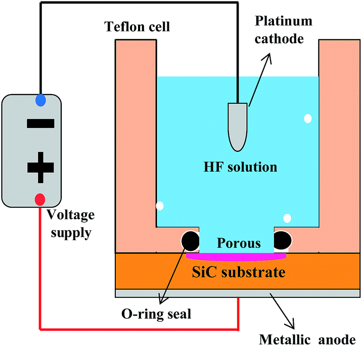 | ||
| Fig. 1 Schematic diagram of the experimental set-up for anodic oxidation process. | ||
To investigate the passivation effect, the Al2O3 films were deposited on the porous samples in an ALD reactor (Model R200, Picosun, Finland), using trimethylaluminium (TMA:Al(CH3)3) and H2O gases as precursors for aluminum and oxygen, respectively. The precursors were alternately pumped into the reaction chamber in the ALD reactor by N2 carrier gas flow with the following sequence: 0.1 s TMA pulse, 3.0 s N2 purge, 0.1 s H2O pulse, and 4.0 s N2 purge. One monolayer will be chemisorbed and retained on the surface of porous structures after one cycle. More details can be found in ref. 12 and 24. To study the passivation performance, 8 nm, 20 nm and 50 nm thick Al2O3 were deposited at 160 °C for samples a2, a3 and a4 respectively. For comparison, samples a5, a6 and a7 were also covered with 8 nm, 20 nm and 50 nm thick Al2O3 deposited at 200 °C. A post-deposition rapid thermal annealing (RTA) treatment of sample a2, a3, a4, a5, a6 and a7 were performed at 450 °C for 30 min in N2 (10 sccm) environment.
The second batch of porous SiC samples (sample b2 to b10) covered with 20 nm thick of Al2O3 were used to optimize the annealing temperature and duration. Finally, 20 nm thick Al2O3 was deposited on the third batch of porous samples c2, c3 and c4 with 3.0, 20.0 and 30.0 s N2 purge time, respectively.
The morphology of the porous SiC before and after passivation was inspected by scanning electron microscopy (SEM). The crystal structure in porous SiC was recorded by X-ray diffraction (XRD). The passivation effect can be observed visually from the enhancement of PL intensity. To investigate the annealing effect on passivation, XPS was used to distinguish the elemental composition. The penetration depth of Al2O3 films in the porous sample was analyzed by using a tunable beam of argon ions, then cycles of sputtering and measurement performed to measure the Al2O3 composition as a function of sample depth.
3. Results and discussion
3.1 Morphology of the porous SiC covered with Al2O3
The cross-sectional SEM images of porous SiC without and with 20 nm thick Al2O3 are shown in Fig. 2. The porous layer contains nano-triangular pores (marked by yellow triangle in Fig. 2(b)) with the size varying from 10–30 nm. The pore morphology varied across the depth of the sample from the triangular to the dotted line. This is attributed to the non-uniformity of the localized electrode potential and electrolyte transportation in deep pore structures. However, the pores structures of porous SiC in this work are more uniform than that fabricated by direct current and without UV illumination.24 The triangular pores line up in an orderly arrangement and then pile up layer by layer. The distance between the two layers is constant. In addition, the neighboring layers are in some cases connected by nearly vertically oriented pores (labeled with an ellipse in Fig. 2(b)). It has been demonstrated that the formed anodized porous layer is single-crystal 6H-SiC.25 Thus, the triangular pore can be used to identify the crystallographic orientation of the preferential etch planes and their variations with depth. Fig. 2(b) also shows very small structures (microcrystallites) between two adjacent pores which conform to the condition of quantum confinement with dimensions of 2–5 nm. However, for 6H-SiC (energy bandgap of 3.1 eV), the luminescence peak of quantum structure should be located in UV range, which will not be investigated in this work. After depositing 20 nm thick Al2O3, the pores in the top layer are almost filled. The passivation boundary is not clearly observed in the SEM image, but it appears that the bottom layer is not covered with Al2O3. The passivation depth will be further investigated by XPS measurement. | ||
| Fig. 2 Cross-sectional SEM images of porous SiC top layer (a) before and (d) after Al2O3 passivation (20 nm). Enlarged view of the top layer before (b) and after passivation (e), and enlarged view of the bottom layer before (c) and after passivation (f). | ||
3.2 X-ray diffraction characterization of porous SiC
The crystal properties of original flat and porous samples have been characterized by XRD patterns using a Rigaku SmartLab® XRD system, with Cu Kα radiation from a Cu source (λ = 1.5406 Å). There are two obvious reflections from the crystal planes of 6H-SiC matrix, as shown in Fig. 3(a). The two main peaks are located at the angles of 35.60° and 75.38°, which corresponding to the planes (006) and (0012) of 6H-SiC, respectively. Details of the intensive XRD peaks located at 35.60° are presented in Fig. 3(b). It could be seen that two additional shoulder peaks (35.40° and 35.80°) appeared in the porous samples. These peaks can be attributed to the reflection from surface inclusions on triangular pores, such as dangling bonds and Si related oxide. After passivated by 20 nm Al2O3, the symmetric shoulder peaks became sharper due to the saturation of dangling bonds.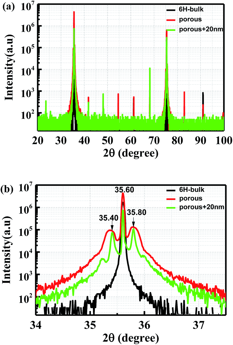 | ||
| Fig. 3 (a) XRD diagram of bulk 6H-SiC, porous sample before and after passivation; (b) high intensity XRD peaks of the samples presented in more details. | ||
3.3 Al2O3 thickness optimization
To optimize the thickness, a layer of 8 nm, 20 nm and 50 nm thick Al2O3 was deposited on porous sample a2, a3 and a4 at 160 °C, respectively. In addition to this, porous samples a5, a6 and a7 were also covered with 8 nm, 20 nm and 50 nm thick Al2O3 deposited at 200 °C, and followed by a 30 min annealing at 450 °C. The passivation effect was characterized by PL measurements using a 375 nm laser as excitation source coupled into a microscope. After passivation, the PL intensity of porous samples a2, a3 and a4 increased by a factor of 105%, 206% and 33% compared to reference sample a1, respectively, as shown in Fig. 4(a). Fig. 4(b) shows that sample a6 also has the largest PL enhancement of 178% among sample a5, a6 and a7. However, the emitting peak of passivated porous samples is red shifted with 50 nm thick Al2O3. The cross-sectional SEM image in Fig. 2(d) shows that 20 nm of Al2O3 already fills the top layer of the porous sample. Excess oxygen atoms in 50 nm thick Al2O3 may oxidize the porous surface and increase the oxygen-related defects during the annealing process, leading to the red shift.24 Therefore, it reveals that the effective passivation thickness is 20 nm for the porous SiC samples. | ||
| Fig. 4 PL spectra of porous SiC covered by 5 nm, 20 nm and 50 nm Al2O3 film deposited at (a) 160 °C and (b) 200 °C. The samples were annealed at 450 °C for 30 min. Sample a1 is the original porous SiC for reference. | ||
3.4 Impact of post-annealing conditions
The surface passivation quality of Al2O3 films grown by ALD was investigated after annealing under various conditions, i.e. annealing with different time and temperatures ranging from 300 °C to 500 °C. Based on the passivation results, all the samples were covered with 20 nm Al2O3 films deposited at 160 °C. Fig. 5 illustrates the passivation effect by PL measurement. Samples b2, b3, b4 and b5 were annealed for 5 min, 15 min, 30 min and 45 min at 450 °C, which resulted in an enhancement by a factor of 5.70, 5.57, 4.63 and 3.99, respectively, as shown in Fig. 5(a). Afterwards, the annealing temperature was also investigated for sample b6, b7, b8, b9 and b10 with 5 min at 300 °C, 350 °C, 400 °C, 450 °C and 500 °C, respectively. In Fig. 5(b), it can be seen that the enhancement for the passivated sample b6, b7, b8, b9 and b10 is 2.79, 5.40, 5.89, 5.70 and 3.03, respectively, compared to the reference sample b1. However, the emission peak of sample b8, b9 and b10 is slightly red shift due to the oxidation effect with higher annealing temperature. The surface passivation performance was found to depend on both the annealing temperature and the duration. For higher annealing temperatures and longer annealing times the passivation performances degrades. It also can be deduced that the emission in porous 6H-SiC is mainly attributed to the surface defects.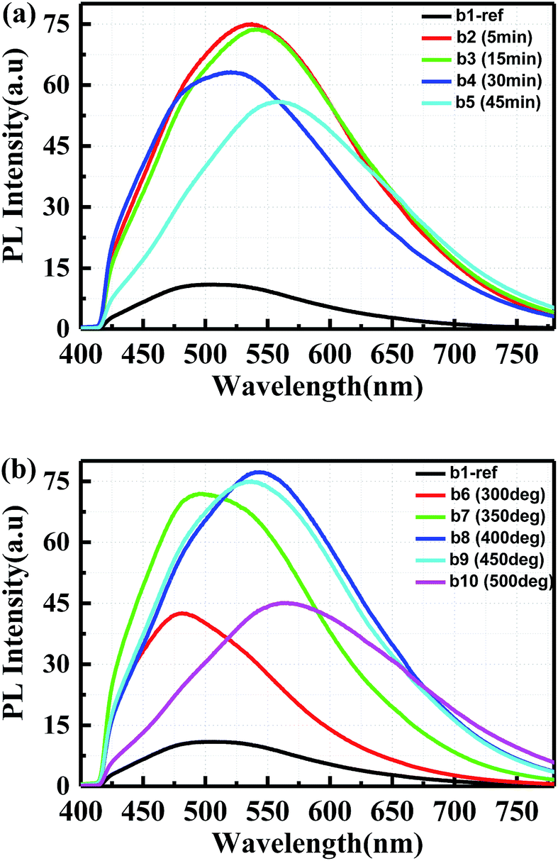 | ||
| Fig. 5 PL spectra in porous SiC samples covered by 20 nm Al2O3 film deposited at 160 °C: (a) sample b2, b3, b4 and b5 were annealed for 5 min, 15 min, 30 min and 45 min at 450 °C, respectively; (b) sample b6, b7, b8, b9 and b10 were annealed at 300 °C, 350 °C, 400 °C, 450 °C and 500 °C for 5 min, respectively. | ||
3.5 Optimization of ALD purge time
From the cross-sectional SEM images in Fig. 2, it can be seen that the pore size is around 15–30 nm and only the pores in the top layer are entirely filled by Al2O3. To verify the ALD penetration depth and how it affects the PL, different purge time in the ALD process was studied. Porous samples c2, c3 and c4 were deposited with the purge time of 3.0 s, 20.0 s and 30.0 s, respectively. The PL spectra are shown in Fig. 6(a) where the original porous sample c1 (40 μm thick of porous layer) is used for reference. After passivation, the PL enhancement for sample c2, c3 and c4 are 3.43, 5.50 and 2.75, respectively. Thus, 30.0 s purge time is too long for the passivation due presumably to oxidation in the ALD react chamber.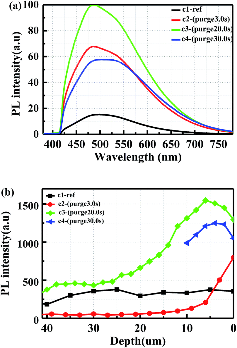 | ||
| Fig. 6 (a) PL and (b) cross-sectional PL spectra in porous SiC covered by 20 nm Al2O3 film deposited with different purge time. The purge time for c2, c3 and c4 is 3.0 s, 20.0 s and 30.0 s, respectively. | ||
The cross-sectional PL distribution was also characterized to inspect the penetration depth, as shown in Fig. 6(b). The excitation laser is guided into a microscope with 20× objective. The acquisition spot size is 1.14 μm, while the collected illumination signal is integration from 520 nm to 600 nm within the same porous depth. Thus the results in the cross-sectional PL are not comparable with that in the normal PL spectra in Fig. 6(a). The distribution curve for reference sample c1 shows that the emitted light intensity is uniform through the porous layer. It can be seen that the PL intensity in sample c3 is higher than the other two samples within the top 6 μm layer. However, the maximum point in sample c3 and c4 is located about 6 μm and 4 μm beneath the surface respectively, which is attributed to the oxidation in the ALD chamber with much longer deposition time. Nevertheless, this trend is used to roughly judge the penetration depth of ALD deposition. A more accurate characterization for the optimized sample c3 will be shown by XPS characterization in the following section.
3.6 X-ray photoelectron spectroscopy characterization
XPS measurements were performed to investigate the passivation mechanisms and Al2O3 penetration depth in porous SiC. Fig. 7 shows Al 2p core-level XPS spectra in as-deposited and annealed porous SiC samples with Gaussian fitting. The pass energy was set to 50.0 eV for the measurements. The spectra were calibrated using C 1s at 284.8 eV as the internal reference to correct for charging. For as-deposited Al2O3 on porous SiC, two components can be observed at the binding energies of 76.04 eV and 76.9 eV, corresponding to Al–O bonds and Al–OH bonds, respectively. After annealing for 5 min, the component at 76.9 eV decreased, indicating the reduction of Al–OH bonds during post-deposition annealing, as shown in Fig. 7(b). It should be noted here that the residual Al–OH bonds existed during ALD deposition, which is easily broken and released within Al2O3 films. These released H atoms play an important role for the passivation performance in the porous layer. Such H atoms will diffuse and arrive at the Al2O3/SiC interface and thus neutralize the dangling bonds.17,23 This phenomenon is in consistent with that in XRD results. | ||
| Fig. 7 XPS core level spectra of Al 2p in porous SiC covered by 20 nm Al2O3 film: (a) as-deposited and (b) after annealing. | ||
In order to characterize the Al2O3 penetration depth, the porous sample c3 was analyzed by XPS with argon ion sputtering time, using ion beam energy of 3 keV. The acquisition spot size for the measurement is 400 μm. The results are shown in Fig. 8. Before sputtering, the intensity of Al 2p peak at 74.5 eV was the mixed signal of Al2O3 and absorbed CO2 on the surface. The peak was slightly shifted to 75.2 eV as the CO2 was sputtered off. However, the Al–O peak in Al 2p remains at the same binding energy location without discernible change with increasing sputtering time. The Al–O peak in O 1s gradually shifts to a higher binding energy with increasing sputtering time, and the intensity also decreases due to the Al2O3 thickness decreasing in the deeper porous layer. Based on the sputtering rate, both Al 2p and O 1s spectra could be used to qualitatively judge the passivation depth. The sputtering depth was measured to be 6.5 μm using a profiler. When zooming in the signal in Al 2p with a sputtering time of 45 min, the signal of Al–O bonds is still present. Thus the penetration depth for porous sample c3 is at least 6.5 μm. Simultaneously, the Si–C signal in C 1s and Si 2p is increased with the sputtering time. In addition, it is accounted for the contamination caused by the air exposure, which leads to bonding of the surface carbon atoms with the oxygen or water molecules from the air.
 | ||
| Fig. 8 XPS high resolution spectra of (a) Al 2p, (b) O 1s, (c) Si 2p and (d) C 1s in porous SiC covered by 20 nm Al2O3: the sputtering ion-beam energy is 3 keV; acquisition spot size is 400 μm, with pass energy of 50 eV. | ||
3.7 Time-resolved PL characterization
To analyze the passivation effect, time-resolved PL measurements were used to characterize the porous samples. The measurements were performed at room temperature. For the excitation, a pulsed diode laser (pulse width ∼ 44 ps, 0.74 mW) working at 375 nm, controlled by a programmable laser driver (LDH-D-C-375 with PDL 820, PicoQuant GmbH), was focused onto the samples through a microscope. A burst mode excitation sequence was used to achieve a good signal-to-noise ratio in the measurement. In the burst mode, a pulse pattern was generated using the PDL 820 laser driver, consisting of 1 laser pulse followed by a waiting period of 62.5 ns, resulting in a total frequency of 16 MHz. The time-resolved PL results are presented in Fig. 9. The mechanisms of lifetime quenching are revealed by the lifetimes of the respective triple-exponential fitting, which includes non-radiative and radiative surface recombination and recombination in bulk SiC. The luminescence decay can be adequately described by triple-exponential fits, as shown in Table 1 and Fig. 9 with dotted lines. The average PL lifetime was calculated by using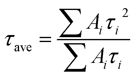 , where τi and Ai (i = 1, 2, 3) represent the lifetime and weight factor of each component.26 The average lifetime in bulk 6H-SiC and porous samples c1, c2, c3 and c4 is 1.89 ns, 0.38 ns, 0.78 ns, 0.65 ns and 0.61 ns, respectively. Surface defects related non-radiative recombination quenches the PL lifetime in the porous samples. As expected the lifetime is susceptible to surface passivation, so the average lifetime in sample c2 increased after passivation. It appears that the increase of ALD purge time results in a decrease of such radiative recombination channels. For longer purge times, the top layer of the porous sample might be oxidized in the ALD chamber thereby decreasing the passivation effect.
 | ||
| Fig. 9 Time-resolved PL (normalized) of flat 6H-SiC, porous samples c1, c2, c3 and c4. The decay curves were fitted with triple-exponential components. | ||
| Samples | τ3 (ns) | A3 | τ2 (ns) | A2 | τ1 (ns) | A1 | τave (ns) |
|---|---|---|---|---|---|---|---|
| 6H-Flat | 11.93 | 0.061 | 2.87621 | 0.7283 | 0.55017 | 12.9097 | 1.8876 |
| c1 | 6.52159 | 0.0185 | 1.80673 | 0.52743 | 0.34148 | 135.8705 | 0.3843 |
| c2 | 9.68234 | 0.01402 | 2.76457 | 0.48112 | 0.51831 | 28.18808 | 0.7815 |
| c3 | 8.27814 | 0.01635 | 2.50885 | 0.50592 | 0.46771 | 39.41452 | 0.6514 |
| c4 | 7.91918 | 0.01458 | 2.38284 | 0.49494 | 0.45355 | 40.98371 | 0.6113 |
4. Conclusions
Porous B–N co-doped SiC samples were prepared by anodic oxidation of 6H-SiC substrate. The PL emission peak is blue shifted to around 520 nm due to surface defects and quantum confinement effect of B–N donor–acceptor-recombination in porous 6H-SiC. The XRD patterns shows shoulder peaks of reflection from surface inclusions on the porous samples. Significant enhancement of the PL intensity was observed from porous SiC after deposition and annealing of ALD Al2O3 films. The thickness, annealing time, annealing temperature, and precursor purge time were optimized in term of strong PL. In order to study the passivation mechanism and penetration depth, XPS measurements were performed to check the chemical bonds in passivated porous SiC. It has been confirmed that the passivation effect is attributed to the OH bonds in Al2O3 films, which suppressed the non-radiative recombination after annealing. Moreover, the average carrier lifetime in Al2O3 passivated samples is longer than original porous SiC. However, there is a trade-off between the passivation and the oxidation effect during ALD deposition and annealing process. As a consequence, we draw the conclusions that the optimized passivation condition for porous SiC is 20 nm thickness of Al2O3, deposited at 160 °C and with a purge time of 20 s, followed by an annealing for 5 min at 350 °C. In addition, the red-shift phenomenon indicates that emission in porous SiC is mainly attributed surface defects. Such fundamental investigation provides valuable information to understand the emission mechanism and improve the emission efficiency in porous SiC based optical applications.Acknowledgements
This work was supported by Innovation Fund Denmark (project No. 4106-00018B).Notes and references
- S. Kamiyama, et al., Fluorescent SiC and its application to white light-emitting diodes, J. Semicond., 2011, 32(1), 013004 CrossRef.
- H. Ou, et al., Advances in wide bandgap SiC for optoelectronics, Eur. Phys. J. B, 2014, 87(3), 58 CrossRef.
- T. Nishimura, et al., High efficiency violet to blue light emission in porous SiC produced by anodic method, Phys. Status Solidi C, 2010, 7(10), 2459–2462 CrossRef CAS.
- T. Matsumoto, et al., Blue-green luminescence from porous silicon carbide, Appl. Phys. Lett., 1994, 64(2), 226–228 CrossRef CAS.
- T. L. Rittenhouse, Surface-state origin for the blueshifted emission in anodically etched porous silicon carbide, J. Appl. Phys., 2004, 95(2), 490 CrossRef CAS.
- Y. Shishkin, et al., Fabrication and morphology of porous p-type SiC, J. Appl. Phys., 2005, 97(4), 044908 CrossRef.
- A. T. Cao, Q. N. T. Luong and C. T. Dao, Influence of the anodic etching current density on the morphology of the porous SiC layer, AIP Adv., 2014, 4(3), 037105 CrossRef.
- M. Leitgeb, et al., A Combination of Metal Assisted Photochemical and Photoelectrochemical Etching for Tailored Porosification of 4H SiC Substrates, ECS J. Solid State Sci. Technol., 2016, 5(10), P556–P564 CrossRef CAS.
- B. Hoex, et al., On the c-Si surface passivation mechanism by the negative-charge-dielectric Al2O3, J. Appl. Phys., 2008, 104(11), 113703 CrossRef.
- W. W. Hsu, et al., Surface passivation of Cu(In,Ga)Se2 using atomic layer deposited Al2O3, Appl. Phys. Lett., 2012, 100(2), 023508 CrossRef.
- B. Dou, et al., Surface passivation of nano-textured silicon solar cells by atomic layer deposited Al2O3 films, J. Appl. Phys., 2013, 114(17), 174301 CrossRef.
- N. Batra, et al., Influence of deposition temperature of thermal ALD deposited Al2O3 films on silicon surface passivation, AIP Adv., 2015, 5(6), 067113 CrossRef.
- G. Agostinelli, et al., Very low surface recombination velocities on p-type silicon wafers passivated with a dielectric with fixed negative charge, Sol. Energy Mater. Sol. Cells, 2006, 90(18–19), 3438–3443 CrossRef CAS.
- G. Dingemans and W. M. M. Kessels, Status and prospects of Al2O3-based surface passivation schemes for silicon solar cells, J. Vac. Sci. Technol., A, 2012, 30(4), 040802 Search PubMed.
- A. Dillon, et al., Surface chemistry of Al2O3 deposition using Al(CH3)3 and H2O in a binary reaction sequence, Surf. Sci., 1995, 322(1), 230–242 CrossRef CAS.
- A. W. Ott, J. W. Klaus, J. M. Johnson and S. M. George, Al2O3 thin film growth on Si (100) using binary reaction sequence chemistry, Thin Solid Films, 1997, 292, 135–144 CrossRef CAS.
- L. Q. Zhu, et al., Atomic layer deposited Al2O3 films for anti-reflectance and surface passivation applications, Appl. Surf. Sci., 2014, 288, 430–434 CrossRef CAS.
- E. Sun, et al., Enhancement of photoluminescence intensity from Si nanodots using Al2O3 surface passivation layer grown by atomic layer deposition, Appl. Surf. Sci., 2010, 256(16), 5021–5024 CrossRef CAS.
- F. Kersten, et al., Role of Annealing Conditions on Surface Passivation Properties of ALD Al2O3 Films, Energy Procedia, 2013, 38, 843–848 CrossRef CAS.
- M. B. González, et al., Charge trapping analysis of Al2O3 films deposited by atomic layer deposition using H2O or O3 as oxidant, J. Vac. Sci. Technol., B: Nanotechnol. Microelectron.: Mater., Process., Meas., Phenom., 2013, 31(1), 01A101 Search PubMed.
- M. Groner, et al., Low-temperature Al2O3 atomic layer deposition, Chem. Mater., 2004, 16(4), 639–645 CrossRef CAS.
- A. Richter, et al., Reaction kinetics during the thermal activation of the silicon surface passivation with atomic layer deposited Al2O3, Appl. Phys. Lett., 2014, 104(6), 061606 CrossRef.
- G. Dingemans, et al., Influence of annealing and Al2O3 properties on the hydrogen-induced passivation of the Si/SiO2 interface, J. Appl. Phys., 2012, 111(9), 093713 CrossRef.
- W. Lu, et al., Fabrication and surface passivation of porous 6H-SiC by atomic layer deposited films, Opt. Mater. Express, 2016, 6(6), 1956 CrossRef.
- J. S. Shor, et al., Direct observation of porous SiC formed by anodization in HF, Appl. Phys. Lett., 1993, 62(22), 2836–2838 CrossRef CAS.
- Y. A. Gromova, et al., Fluorescence energy transfer in quantum dot/azo dye complexes in polymer track membranes, Nanoscale Res. Lett., 2013, 8(1), 452 CrossRef PubMed.
| This journal is © The Royal Society of Chemistry 2017 |