
 Open Access Article
 This Open Access Article is licensed under a
 Creative Commons Attribution 3.0 Unported Licence
Ultra-thin ultraviolet cathodoluminescent device based on exfoliated hexagonal boron nitride†
Dongju Leea and
Sung Ho Song *b
*b
aNuclear Materials Development Division, Korea Atomic Energy Research Institute, 989-111 Daedeok-daero, Yuseong-gu, Daejeon, 34057, Republic of Korea
bDivision of Advanced Materials Engineering, Kongju National University, Chungnam 330-717, Republic of Korea. E-mail: shsong805@kongju.ac.kr
First published on 23rd January 2017
Abstract
The need for highly efficient devices with longer operating lives in the blue wavelength region is increasing. Herein, we showed that hexagonal boron nitride, as a blue luminescent material, is promising because it is a wide bandgap semiconductor with very high thermal and chemical stabilities and can be used in devices operating under extreme conditions. Specifically, through the highly luminous properties of exfoliated hexagonal boron nitride (Exf-hBN), a blue emission device equipped with a field-emission array using carbon nanotube as an excitation source was fabricated and its stable operation has been demonstrated. Furthermore, the cathodoluminescent device is thinner than conventional lamps when using the ultra-thin Exf-hBN film and graphene as an electrode. The blue fluorescence of Exf-hBN may allow new devices to be developed with extraordinary properties for applications from optoelectronics to biotechnological devices.
1. Introduction
Recently, a number of layered materials with reduced dimensions have drawn the interest of researchers due to their remarkable optical properties, which are different from their bulk properties. Recently, the luminous 2D materials have been used in industrial applications, such as light emission displays, and the low-energy cathodoluminescence (CL) is a crucial property for this purpose. Furthermore, luminous modulation by local variations in the 2D materials has gained importance for the development of 2D optical and optoelectronics devices.Hexagonal boron nitride (h-BN) is a conventional and harmless material with unique properties such as a wide bandgap, low-dielectric constant, high thermal conductivity, and chemical inertness.1–5 Since the first observation of an intense UV exciton emission that made this material a candidate in light-emitting devices,6 the emergence of fluorescent h-BN shows promise as a new class of optical materials for light emission devices in the UV region at 5.8 eV with a single strong excitonic emission. Accordingly, understanding the electronic band, exciton structure, and the nature of intrinsic defects in the h-BN layers of h-BN becomes even more important.7,8 More recently, many researchers have demonstrated that the residual impurities and defects form the photoactive states within the h-BN bandgap.9,10 During the last decade, h-BN has been studied using far-UV properties,6,8,10 optical properties,11–14 X-ray emission and absorption,15–22 interband transitions and plasmons.23–26 Therefore, research continues on the band gap energies of h-BN by quality and experimental methods due to the arguments on the high emission of free exciton luminescence. Recently, Watanabe et al.5 have measured the direct bandgap energy and exciton binding energy of h-BN. Perera et al.20 assumed using theoretical calculations that h-BN is an indirect bandgap material (5.95 eV) and has a lowest direct interband transition at 6.47 eV. Moreover, the energy transfer to defects and impurities may suppress these intrinsic transitions and affect the luminescent properties in polycrystalline samples. Generally, the presence of structural defects related to impurities, low-quality crystals, and strain generates the additional emissions. Therefore, h-BN with various levels of structural defects make it possible to realize a blue emission device with a structure similar to that of a conventional field emitting device in the visible region. However, to date, these studies have been limited due to several drawbacks including the difficulty in controlling the fluorescence and their limited applications.
To confirm the possibility of optoelectronic applications using exfoliated h-BN, for the first time, we directly employed them as emitters in a blue emission device. Herein, we studied the potential of liquid-exfoliated h-BN (Exf-hBN) with structural defects as a fluorescent material by fabricating a blue emission device.27 The hexagonal structure of h-BN makes it a two-dimensional material using a liquid exfoliation process and the defect levels, such as intrinsic B or N defects, impurities or generic structural defects, of h-BN increase using the exfoliation process. This device uses field-emission cold cathodes using carbon nanotube (CNT) to obtain a long lifetime and high stability because the cold cathode emits electrons at a lower operating temperature and voltage than a hot cathode. Moreover, the cathodoluminescent device is thinner than the conventional lamps when using the ultra-thin Exf-hBN film and graphene as an electrode. Therefore, these results not only validate the use of a blue luminous h-BN device as a possible alternative to conventional lamp sources, but also shows its potential to contribute to various optoelectronic applications.
2. Experimental
Exfoliation of h-BN
Exf-hBNs were prepared via the liquid exfoliation of h-BN micro-sized particles. In a typical experiment, BN powder (100 mg, KOJUNDO KOREA CO., LTD, used as received) was sonicated for 10 h in isopropyl alcohol (IPA, 500 mL, Merck). The dispersed BN solution was then centrifuged at 7000 rpm for 15 min to remove the aggregates and thick flakes.Preparation of the ultra-violet cathodoluminescence device
A CNT field emitter cathode was fabricated using CNT/Ag nanocomposite powders. The CNT/Ag nanocomposite powders were synthesized via molecular mixing after which the CNTs were functionalized via acid treatment. The functionalized CNTs and silver nitrate were dispersed in ethylene glycol via ultrasonication. Hydrazine was then added to the mixture of CNT and silver nitrate solutions after which the mixture was refluxed for 2 h at 60 °C. The CNT/Ag nanocomposite powders were washed with ethanol and dried under vacuum. The CNT/Ag nanocomposite powders were deposited on a 0.5 mm-thick SUS 304 plate via spray coating. The substrate was then sintered for 30 min at 400 °C under vacuum. To activate the emission tips, taping was carried out. The ultraviolet cathodoluminescence anode was prepared via the deposition of graphene and Exf-hBN on a quartz substrate. Graphene was grown on 25 μm thick Cu foils (Alfa Aesar, item no. 13 382) in a tube furnace with H2 (10 sccm) and CH4 (60 sccm) at 1000 °C for 20 min. Graphene on the other side of the Cu foil was removed using O2 plasma. Cu foil was dissolved in an aqueous solution (0.1 M ammonium persulfate) to detach graphene from the Cu foil. The graphene films were then transferred and dried on a quartz substrate. Exf-hBN was deposited on graphene by spray coating.Characterization
The morphologies of the Exf-hBN were investigated by TEM (JEOL JEM-2200FS). Raman spectroscopy and AFM analysis were performed using a Senterra system (Bruker) coupled with a customized AFM module. The microstructure and cathodoluminescence were measured using field-emission scanning electron microscopy (FE-SEM) (Philips XL 30 SEM) with a MonoCL4 System (Gatan). The chemical composition was measured by Fourier transform infrared (FT-IR) spectroscopy (Jasco FT/IR-4100 Type-A, ATR mode). X-ray photoelectron spectroscopy and ultraviolet photoelectron spectroscopy experiments were performed using a Sigma Probe (Al Kα; Thermo Scientific, Hudson, NH, USA). A silicon substrate was used for the XPS experiments and the binding energy was calibrated with reference to the C 1s energy at 284.5 eV. The optical properties of Exf-hBN were determined using a UV-3101PC spectrometer and photoluminescence spectra (VUV PL measurement system, 147 nm krypton lamp as excitation source). The field emission was measured in a high-vacuum chamber at a base pressure of 10−7 Torr. The distance between the cathode and anode was maintained at 300 μm and a voltage of up to 1000 V was applied to the cathode.3. Results and discussion
Fig. 1a schematically illustrates the procedure for the exfoliation of micro-sized BN particles. Liquid exfoliation was used to expose the layered material to ultrasonic waves in a solvent. These waves generate cavitation bubbles that collapse into high-energy jets, breaking up the layered crystallites to produce exfoliated nanosheets. The surface energy of the solvent is similar to that of the layered material, the energy difference between the exfoliated and reaggregated states is very small, which removes the driving force for reaggregation.28,29 From this method, the yield of the BN nanosheets was about ∼1 wt% and the concentration of the dispersed Exf-hBNs obtained in IPA was 0.004 mg mL−1. The morphology and structural properties of Exf-hBN obtained from the liquid exfoliation were examined by atomic force microscopy (AFM) and transmission electron microscopy (TEM). Fig. 1b is a representative AFM topography image of Exf-hBN. The flake shows a lateral size of 40–100 nm and height of 2.7 nm, which corresponds to the height of few-layered boron nitride. Fig. 1c shows the representative TEM image, which also shows that the Exf-hBN is mono or few-layers due to the observation of the fringe pattern at the edge of the flake via high-resolution TEM. Moreover, the typical hexagonal pattern obtained from the SAED data, as shown in the inset of Fig. 1c, shows that the crystallinity of the Exf-hBN was not degraded during the exfoliation process.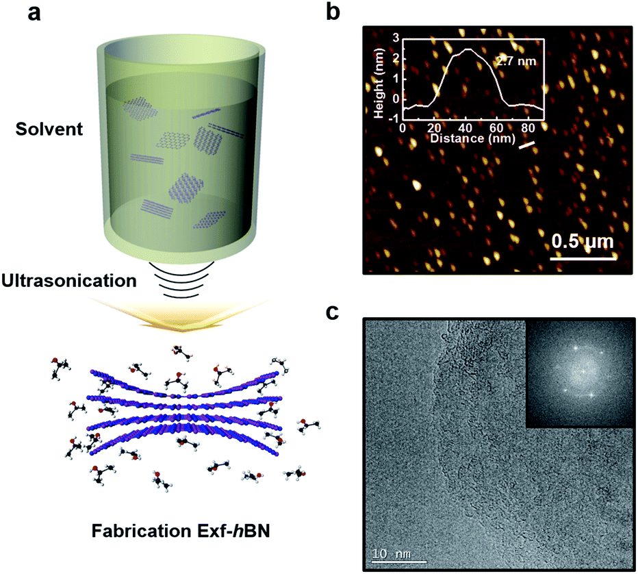 | ||
| Fig. 1 A schematic showing the overall process and characterization of Exf-hBN. (a) A schematic of the strategy used to prepare Exf-hBN. (b) An AFM image of Exf-hBN on a mica substrate. (c) The HRTEM image and fringe patterns of Exf-hBN. | ||
Fig. 2 shows the XPS spectra, i.e. survey and narrow scans of the elemental lines with the results of curve fitting. The binding energy of other elements was calibrated with reference to C 1s at 284.5 eV In the XPS spectra of Exf-hBN, the peaks at 190.1, 284.5, 397.8, and 532.4 eV correspond to B 1s of Exf-hBN, C 1s of adsorbed carbon, N 1s of Exf-hBN, and O 1s of Exf-hBN, respectively. Fig. 2b indicates the B 1s core level spectrum that was fitted to one component. The main component at 190.1 eV corresponds to the B–N bond. The N 1s spectrum shown in Fig. 2c can also be fitted with one curve at a binding energy of 397.8 eV and corresponds to the B–N bond.30,31 Fig. 2d shows the Raman spectra of the Exf-hBN. Initially, for bulk h-BN, the Raman peak occurs at ≈1366 cm−1, which exhibits a characteristic peak due to the E2g phonon mode.32,33 After the exfoliation process, it was found to result in the E2g phonon mode centered at approximately 1369 cm−1, with a blue-shift of ∼3 cm−1. This behavior is explained by the elongation of the B–N bonds in bulk h-BN due to the interlayer interactions, which leads to softening of the phonons, relative to monolayer h-BN where the influence of the interlayer interactions is absent and the B–N bond are expected to be shortened.32,34,35 Following exfoliation, the FWHM value of the band at 1369 cm−1 was 10.5 cm−1, whereas that of the band at 1366 cm−1 in the h-BN starting material was 8.7 cm−1. This substantial change was attributed to a decrease in the superposition of multiple peaks.33 The observed differences in the phonon frequency of the E2g mode before and after the exfoliation procedure support the assertion that mono- or few-layered BNs are formed during the exfoliation process.
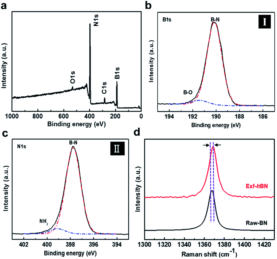 | ||
| Fig. 2 A comparison of the properties of Exf-hBN and Raw-BN. (a) XPS survey scan of Exf-hBN. (b) The high-resolution XPS B 1s spectra of Exf-hBN. (c) High-resolution XPS N 1s spectra of Exf-hBN. (d) The Raman spectra of Exf-hBN and Raw-BN. | ||
The oxygen bonding state of Exf-hBN was examined using X-ray photoelectron spectroscopy (XPS); the XPS spectrum is shown in Fig. 3a. In the O 1s narrow scan with fitted curves, the peaks at 532.4 eV were assigned to the B–O bonds (sp3-hybridized N3B(OH)) that may have formed during ultrasonication, which indicate the presence of numerous oxygen functional groups on Exf-hBN due to structural defects.36 The degree of oxidation was slightly increased by increasing the ultrasonication time when compared with that of the as-received BN powders (from 1.3 at% to 1.7 at% oxygen composition). From the Fourier transform infrared spectroscopy (FT-IR) analysis of Raw-BN and Exf-hBN (Fig. 3b), the characteristic peaks related to the B–O (1190 cm−1) and B–O–H band (1020 cm−1) are observed in Exf-hBN, whereas the oxygen band is absent in Raw-BN. Further analysis of the XPS and FT-IR results shows that the oxygen moieties remain on the surface of Exf-hBN due to the structural defects and impurities. The UV-vis absorption spectrum of the Exf-hBN thin film transferred onto a quartz substrate is shown in Fig. S1a† and demonstrates a small absorbance in the visible region with a significant absorbance only in the UV region. The optical band gap estimated from the UV-vis spectrum of Exf-hBN was about 5.45 eV, as shown in Fig. S1b.†37,38 Furthermore, to confirm the proposed PL properties, the photoluminescence excitation (PLE) spectra were obtained at the maximum PL peak position of Exf-hBN, as shown in Fig. S2.† Exf-hBN exhibits distinct PLE peaks at 240 nm and 280 nm due to the structural defects and impurities. The photoluminescence (PL) of Exf-hBN and Raw BN excited under ambient conditions are shown in Fig. 3c. Though the shapes of the two spectra are same, the PL intensities are increased even more in the Exf-hBN sample during the PL under excitation at 147 nm based on the UV-vis spectrum. Generally, the optical properties of h-BN are known to be strongly affected by oxygen and nitrogen vacancies, which serve as activation, recombination, adsorption, and photosensitivity centers.39,40 Moreover, they have been attributed to a free carrier recombination at the deep impurity levels within the h-BN band gap.41,42 Therefore, during the PL under excitation at 147 nm, as shown in Fig. 3c, Exf-hBN shows a strong peak at ∼325 nm (blue emission), whereas Raw-BN displays a weak peak at 315 nm. The cathodoluminescence (CL) of the Exf-hBN and Raw-BN samples was analyzed at room temperature using an optical system installed on a high-resolution FE-SEM, as shown in Fig. 3d and S3.† The CL spectra and SEM images at different areas of the Exf-hBN are shown in Fig. S3.† In Fig. 3d, the relative intensities of the cathodoluminescence of Exf-hBN were enhanced by the presence of structural defects when compared to those of the Raw-BN sample. This enhancement confirms the previous observation on single h-BN crystals reported by Kubota et al.43 and is consistent with their interpretation of the structural defects. It can be viewed as an indicator of the defect density, as introduced by Watanabe et al.5 Therefore, when compared to Raw-BN, Exf-hBN shows a stronger CL emission.
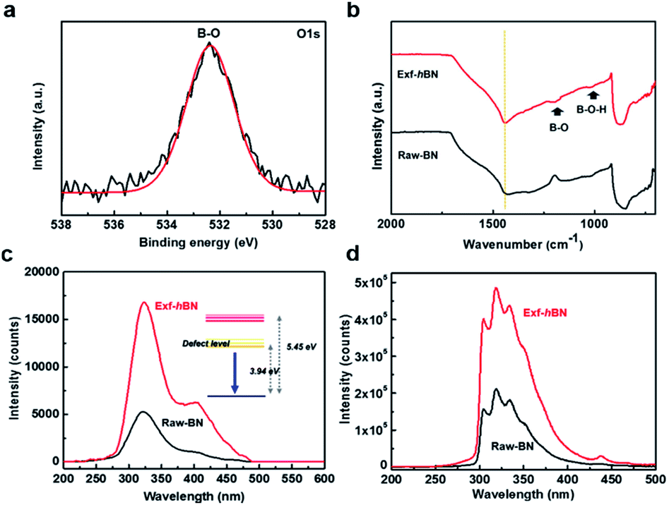 | ||
| Fig. 3 A comparison of the properties of Exf-hBN and Raw-BN. (a) The high-resolution XPS O 1s spectra of Exf-hBN. (b) The FT-IR spectra of Exf-hBN and Raw-BN. (c) The PL spectra of the Exf-hBN and Raw-BN under excitation at 310 nm. (d) The CL spectra of the Exf-hBN and Raw-BN. | ||
Fig. 4a shows a schematic of the ultraviolet cathodoluminescent device structure based on Exf-hBN as the luminescence source. The quartz plate was transparent in the UV region and graphene was used as a transparent electrode. Fig. 4b and c show the digital images of the graphene films transferred on a quartz substrate and the Exf-hBN film deposited on graphene via spray coating, respectively. The three-dimensional AFM surface image of Exf-hBN deposited on the graphene-quartz substrate is shown in Fig. S4.† The surface morphology was found to homogeneously evolve with well-distributed structures. Fig. 4d shows the surface of the CNT/Ag structured field emitter after sintering. During the sintering, the melted Ag nanoparticles flowed to the interface between the CNT and the substrate, and then formed a metal layer. The metal layer increased the bonding strength between the CNT and the substrate, which can help increase the life of the field emitter. The digital image shown in Fig. 4e presents the actual assembly of the ultraviolet cathodoluminescent device in a high-vacuum chamber. A voltage of up to 1000 V was applied to the cathode, as shown in Fig. S5.† Fig. 4f shows the output spectra of the devices. The spectra show an emission peak at 350 nm due to the structural defects and impurities.44,45 The Exf-hBN was used as a fluorescent screen to enable the blue luminescence light to efficiently exit. Furthermore, a long-term duration test on the device at an accelerating voltage of 900 V was also carried out, as shown in Fig. S6.† The UV emission device under the excitation conditions has a lifetime of several tens of hours under stable operating conditions. The field-emission performance parameters of several emitting materials previously reported in the literature are listed in Table S1† for a comparison of their lifetime. Therefore, it is expected that the UV emission device using Exf-hBN can be extended using a field emission device with a longer lifetime.
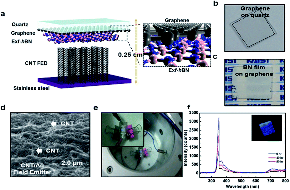 | ||
| Fig. 4 The ultraviolet cathodoluminescent device characteristics of Exf-hBN. (a) A schematic of the ultraviolet cathodoluminescent device structure. (b) Digital images of graphene films transferred on a quartz substrate. (c) A digital image of the Exf-hBN film deposited on graphene via spray coating. (d) The SEM image of the CNT/Ag field emitter. (e) A digital image of the actual assembly of the ultraviolet cathodoluminescent device in a high-vacuum chamber. (f) The output spectra of the ultraviolet cathodoluminescent device. | ||
4. Conclusions
In this study, we demonstrated a novel blue emission device using exfoliated Exf-hBN with high luminescence efficiency as a cathodoluminescent material. The Exf-hBN cathodoluminescent device irradiates a blue emission at 350 nm at an accelerating voltage of 900 V. Furthermore, the lifetime of the device may be longer than several tens of hours under stable conditions via a field emission array using CNT. Moreover, the cathodoluminescent device is thinner than conventional lamps when using the ultra-thin Exf-hBN film and graphene as an electrode. Therefore, the blue emission device with handy size and stable operation can be used as an alternative to conventional lamps. The blue fluorescence of h-BN may allow new devices to be developed with extraordinary properties for applications from optoelectronics to biotechnological devices.Notes and references
- K. Watanabe, T. Taniguchi, T. Kuroda and H. Kanda, Appl. Phys. Lett., 2006, 89, 141902 CrossRef.
- K. Watanabe, T. Taniguchi, T. Kuroda and H. Kanda, Diamond Relat. Mater., 2006, 15, 1891–1893 CrossRef CAS.
- K. Watanabe, T. Taniguchi and H. Kanda, Phys. Status Solidi A, 2004, 201, 2561–2565 CrossRef CAS.
- P. Jaffrennou, J. Barjon, J.-S. Lauret, B. Attal-Trétout, F. Ducastelle and A. Loiseau, J. Appl. Phys., 2007, 102, 116102 CrossRef.
- K. Watanabe, T. Taniguchi and H. Kanda, Nat. Mater., 2004, 3, 404–409 CrossRef CAS PubMed.
- J. Hecht, Laser Focus World, 2008, 44, 67–71 CAS.
- A. Khan, K. Balakrishnan and T. Katona, Nat. Photonics, 2008, 2, 77–84 CrossRef CAS.
- N. Shuji, S. Masayuki, N. Shin-ichi, I. Naruhito, Y. Takao, M. Toshio, K. Hiroyuki and S. Yasunobu, Jpn. J. Appl. Phys., 1996, 35, L74 Search PubMed.
- S. Nakamura, M. Senoh, S.-i. Nagahama, N. Iwasa, T. Yamada, T. Matsushita, H. Kiyoku, Y. Sugimoto, T. Kozaki, H. Umemoto, M. Sano and K. Chocho, Appl. Phys. Lett., 1998, 72, 211–213 CrossRef CAS.
- M. G. Silly, P. Jaffrennou, J. Barjon, J. S. Lauret, F. Ducastelle, A. Loiseau, E. Obraztsova, B. Attal-Tretout and E. Rosencher, Phys. Rev. B: Condens. Matter Mater. Phys., 2007, 75, 085205 CrossRef.
- D. M. Hoffman, G. L. Doll and P. C. Eklund, Phys. Rev. B: Condens. Matter Mater. Phys., 1984, 30, 6051–6056 CrossRef CAS.
- R. Geick, C. H. Perry and G. Rupprecht, Phys. Rev., 1966, 146, 543–547 CrossRef CAS.
- S. N. Grinyaev, F. V. Konusov, V. V. Lopatin and L. N. Shiyan, Phys. Solid State, 2004, 46, 435–441 CrossRef CAS.
- Z. Remes, M. Nesladek, K. Haenen, K. Watanabe and T. Taniguchi, Phys. Status Solidi A, 2005, 202, 2229–2233 CrossRef CAS.
- A. Mansour and S. E. Schnatterly, Phys. Rev. B: Condens. Matter Mater. Phys., 1987, 36, 9234–9240 CrossRef CAS.
- R. D. Carson and S. E. Schnatterly, Phys. Rev. Lett., 1987, 59, 319–322 CrossRef CAS PubMed.
- J. B. MacNaughton, A. Moewes, R. G. Wilks, X. T. Zhou, T. K. Sham, T. Taniguchi, K. Watanabe, C. Y. Chan, W. J. Zhang, I. Bello, S. T. Lee and H. Hofsäss, Phys. Rev. B: Condens. Matter Mater. Phys., 2005, 72, 195113 CrossRef.
- J. Serrano, A. Bosak, R. Arenal, M. Krisch, K. Watanabe, T. Taniguchi, H. Kanda, A. Rubio and L. Wirtz, Phys. Rev. Lett., 2007, 98, 095503 CrossRef CAS PubMed.
- J. A. Carlisle, E. L. Shirley, L. J. Terminello, J. J. Jia, T. A. Callcott, D. L. Ederer, R. C. C. Perera and F. J. Himpsel, Phys. Rev. B: Condens. Matter Mater. Phys., 1999, 59, 7433–7445 CrossRef CAS.
- J. J. Jia, T. A. Callcott, E. L. Shirley, J. A. Carlisle, L. J. Terminello, A. Asfaw, D. L. Ederer, F. J. Himpsel and R. C. C. Perera, Phys. Rev. Lett., 1996, 76, 4054–4057 CrossRef CAS PubMed.
- B. M. Davies, F. Bassani, F. C. Brown and C. G. Olson, Phys. Rev. B: Condens. Matter Mater. Phys., 1981, 24, 3537–3546 CrossRef CAS.
- F. C. Brown, R. Z. Bachrach and M. Skibowski, Phys. Rev. B: Solid State, 1976, 13, 2633–2635 CrossRef CAS.
- C. Tarrio and S. E. Schnatterly, Phys. Rev. B: Condens. Matter Mater. Phys., 1989, 40, 7852–7859 CrossRef CAS.
- R. D. Leapman, P. L. Fejes and J. Silcox, Phys. Rev. B: Condens. Matter Mater. Phys., 1983, 28, 2361–2373 CrossRef CAS.
- R. D. Leapman and J. Silcox, Phys. Rev. Lett., 1979, 42, 1361–1364 CrossRef CAS.
- B. Arnaud, S. Lebègue, P. Rabiller and M. Alouani, Phys. Rev. Lett., 2006, 96, 026402 CrossRef CAS PubMed.
- C. A. Spindt, I. Brodie, L. Humphrey and E. R. Westerberg, J. Appl. Phys., 1976, 47, 5248–5263 CrossRef CAS.
- V. Nicolosi, M. Chhowalla, M. G. Kanatzidis, M. S. Strano and J. N. Coleman, Science, 2013, 340, 1226419–1226437 CrossRef.
- J. N. Coleman, Acc. Chem. Res., 2013, 46, 14–22 CrossRef CAS PubMed.
- D. Lee, S. H. Song, J. Hwang, S. H. Jin, K. H. Park, B. H. Kim, S. H. Hong and S. Jeon, Small, 2013, 9, 2602–2610 CrossRef CAS PubMed.
- K. H. Oh, D. Lee, M. J. Choo, K. H. Park, S. Jeon, S. H. Hong, J. K. Park and J. W. Choi, ACS Appl. Mater. Interfaces, 2014, 6, 7751–7758 CAS.
- R. V. Gorbachev, I. Riaz, R. R. Nair, R. Jalil, L. Britnell, B. D. Belle, E. W. Hill, K. S. Novoselov, K. Watanabe, T. Taniguchi, A. K. Geim and P. Blake, Small, 2011, 7, 465–468 CrossRef CAS PubMed.
- T. Sainsbury, A. Satti, P. May, Z. Wang, I. McGovern, Y. K. Gun’ko and J. Coleman, J. Am. Chem. Soc., 2012, 134, 18758–18771 CrossRef CAS PubMed.
- L. Song, L. Ci, H. Lu, P. B. Sorokin, C. Jin, J. Ni, A. G. Kvashnin, D. G. Kvashnin, J. Lou, B. I. Yakobson and P. M. Ajayan, Nano Lett., 2010, 10, 3209–3215 CrossRef CAS PubMed.
- S. Reich, A. C. Ferrari, R. Arenal, A. Loiseau, I. Bello and J. Robertson, Phys. Rev. B: Condens. Matter Mater. Phys., 2005, 71, 205201 CrossRef.
- D. Lee, B. Lee, K. H. Park, H. J. Ryu, S. Jeon and S. H. Hong, Nano Lett., 2015, 15, 1238–1244 CrossRef CAS PubMed.
- T. H. Yuzuriha and D. W. Hess, Thin Solid Films, 1986, 140, 199–207 CrossRef CAS.
- D. A. Evans, A. G. McGlynn, B. M. Towlson, M. Gunn, D. Jones, T. E. Jenkins, R. Winter and N. R. J. Poolton, J. Phys.: Condens. Matter, 2008, 20, 075233 CrossRef.
- S. H. Song, B. H. Kim, D.-H. Choe, J. Kim, D. C. Kim, D. J. Lee, J. M. Kim, K. J. Chang and S. Jeon, Adv. Mater., 2015, 27, 3152–3158 CrossRef CAS PubMed.
- S. H. Song, M.-H. Jang, J. Chung, S. H. Jin, B. H. Kim, S.-H. Hur, S. Yoo, Y.-H. Cho and S. Jeon, Adv. Opt. Mater., 2014, 2, 1016–1023 CrossRef CAS.
- S. Itoh, M. Tanaka, T. Tonegwa, M. Taniguchi, K. Otsu, T. Niiyama, K. Tamura, M. Namikawa, Y. Naito, Y. Obara, M. Toriumi, M. Kitada, Y. Takeya, K. Deguchi, S. Kawata, Y. Sato, F. Kataoka, H. Toki, K. Sakurada and T. Yamaura, J. Soc. Inf. Disp., 2007, 15, 1057–1064 CrossRef CAS.
- L. Museur, D. Anglos, J.-P. Petitet, J.-P. Michel and A. V. Kanaev, J. Lumin., 2007, 127, 595–600 CrossRef CAS.
- Y. Kubota, K. Watanabe, O. Tsuda and T. Taniguchi, Science, 2007, 317, 932–934 CrossRef CAS PubMed.
- L. Museur and A. Kanaev, J. Appl. Phys., 2008, 103, 103520 CrossRef.
- L. Museur, E. Feldbach and A. Kanaev, Phys. Rev. B: Condens. Matter Mater. Phys., 2008, 78, 155204 CrossRef.
Footnote |
| † Electronic supplementary information (ESI) available: Further details of the UV-vis absorption and photoluminescence excitation spectra of Exf-hBN; the SEM and cathodoluminescence image of Exf-hBN; the three-dimensional AFM surface image of Exf-h-BN film; the emission current and applied voltage characteristic curves obtained for the CNT/Ag field emitter; a digital image of the long-term duration test on the device at an accelerating voltage of 900 V. See DOI: 10.1039/c6ra27279g |
| This journal is © The Royal Society of Chemistry 2017 |