
 Open Access Article
 This Open Access Article is licensed under a
 Creative Commons Attribution 3.0 Unported Licence
A first principles study of the interaction between two-dimensional black phosphorus and Al2O3 dielectric
Jie Suna,
Na Lin *a,
Cheng Tanga,
Hao Renb and
Xian Zhao*a
*a,
Cheng Tanga,
Hao Renb and
Xian Zhao*a
aState Key Laboratory of Crystal Materials, Shandong University, 250100 Jinan, Shandong, PR China. E-mail: linnakth@gmail.com; xianzhao@sdu.edu.cn
bState Key Laboratory of Heavy Oil Processing & Center for Bioengineering and Biotechnology, China University of Petroleum (East China), 266580 Qingdao, PR China
First published on 1st March 2017
Abstract
The chemical degradation of exfoliated black phosphorus (BP) when exposed to ambient conditions can be effectively suppressed via the deposition of Al2O3 dielectric on the BP surface. A good understanding of the interactions between the BP layer and Al2O3 dielectric is important for practical device applications. In the presented paper, first principles calculations have been performed to study the structural, energetic, and electronic properties of BP on an Al-terminated and hydroxylated Al2O3 (0001) surface. Our calculations indicate the band gap of monolayer BP is enlarged by about 160 meV and 92 meV after the deposition respectively of an Al-terminated and hydroxylated Al2O3 surface, which is mainly due to interlayer charge transfer between the BP and Al2O3 surfaces. However, this trend for increasing band gap is inverted upon increasing the number of BP layers. Besides, the valence-band offset of a few-layer (2–4 layer) BP/Al2O3 system is about 0.5–0.9 eV larger than that of a monolayer BP/Al2O3 system, which is more suitable for creating an injection barrier. Moreover, the band gaps of BP/Al2O3 systems could be tuned using an external electric field for practical applications.
Introduction
Two-dimensional (2D) black phosphorus (BP) has been studied intensively due to its unique electronic structure and potential for application in nanodevices.1–3 In contrast to gapless graphene, BP presents a direct band gap that is capable of manifesting large ON/OFF ratios when being used as a channel material in a field effect transistor (FET).4 Meanwhile, its relatively high mobility compared with transition metal dichalcogenides (TMDCS) also makes it an appealing candidate for future devices.5 In addition, the layer-sensitive band gap of BP varies with thickness, from ∼2 eV for a single layer (termed phosphorene) to ∼0.3 eV in bulk form, opening up new opportunities for optoelectronic applications.6–8Despite the praise for BP seeming promising, the nature of defects,9,10 contacts11,12 and chemical stability13,14 in 2D BP are still problematic for realistic device applications. Exfoliated BP flakes have been found to chemically degrade upon exposure to ambient conditions.15,16 Therefore, effective protection to prevent the degradation process is critical for 2D BP. Devices, including carbon nanotube and graphene field-effect transistors (FETs), have exhibited improved performance following encapsulation.17–19 To date, many efforts toward BP surface encapsulation have been reported. For example, recent experiments show that a BP device encapsulated with hexagonal boron nitride (h-BN) possesses high field-effect mobility (∼1350–4000 cm2 (V s)−1) and can be stable under an ambient atmosphere for more than 1 week.20 In addition, Al2O3, which has been considered as a suitable dielectric layer for graphene21 and TMDCS,22 has also been used as a passivation layer in recent BP transistors.23 Luo et al.24 and Wood et al.16 have mentioned that Al2O3 passivated few-layer BP FETs can be stable in air for more than 100 hours.
Although it is a promising idea to use BN or Al2O3 as a capping layer to protect BP, some fundamental issues, such as interface bonding, charge transfer, band gap change, and band alignment, remain little understood. For device applications based on BN/BP and Al2O3/BP, understanding these fundamental issues is of high importance and essential. Recent theoretical investigations25 have demonstrated that BN can be used not only as an effective capping layer to protect BP from chemical degradation, maintaining its major electronic characteristics, but also as an active layer to tune the carrier dynamics and optical properties of BP. However, investigations into the physical properties of Al2O3/BP interfaces are still lacking. Recently, Shao et al.26 have constructed a bilayer Al-terminated Al2O3 surface model to study the interactions between monolayer BP and Al2O3. They found that the electronic properties of BP were severely changed due to bond formation between the BP and Al2O3 surfaces. Nevertheless, BP on a single layer Al terminated Al2O3 surface, which has been demonstrated to be the most stable model of an Al2O3 (0001) surface27 and forms no bond with graphene,21 is yet to be addressed. Besides, the behavior of BP on Al2O3 under a finite electric field is still unclear.
Based on the unexplored issues mentioned above, first principles calculations were carried out in the presented paper to investigate the interactions between BP and Al2O3 surfaces. The most stable configurations were determined by calculating the formation energy of BP/Al2O3 hybrid systems. The layer distances and charge transfer characteristics between BP and Al2O3 surfaces were also involved. The electronic properties of BP affected by the Al2O3 surface were revealed and band-gap modulations of BP/Al2O3 systems under an external electric field were also investigated.
Computational details
First principles calculations were performed based on density functional theory (DFT) implemented in the Vienna ab initio simulation package (VASP).28 The projector-augmented wave (PAW) method was used to describe electron–ion interactions. The generalized gradient approximation in its Perdew, Burke, and Ernzerhof form (GGA-PBE)29 was used for the exchange–correlation part of electron–electron interactions. The van der Waals (vdW) correction proposed by Grimme (DFT-D2)30 was chosen to describe long-range interactions. Two relatively stable configurations of an Al2O3 (0001) surface, namely, a single layer Al-terminated and a fully hydroxylated Al2O3 (0001) surface (Fig. 1), were considered in our work. The Al2O3 (0001) surface was modeled using a slab containing six oxygen O layers and 12 or 11 aluminum layers (depending on the specific surface studied). The second surface of the slab was passivated using pseudo H atoms. The plane-wave energy cutoff was set to 400 eV. A vacuum layer larger than 20 Å was used to avoid interactions between periodic images. Monkhorst–Pack k-points of 4 × 10 × 1 were used for sampling in the first Brillouin zone during geometry optimizations. All geometry structures were fully relaxed until the energy and force were converged respectively to 10−6 eV and 0.01 eV Å−1. The dipolar correction has been included.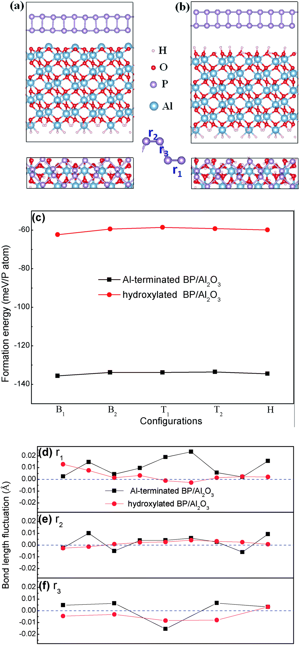 | ||
| Fig. 1 Side and top views of optimized structures of BP on (a) Al-terminated, and (b) fully hydroxylated Al2O3 (0001) surfaces. (c) The formation energies of BP adsorbed on different adsorption sites of the Al-terminated and hydroxylated Al2O3 surfaces. (d)–(f) Bond length alternations of BP interacting with and without a substrate. | ||
The formation energy is defined as Ef = (Etot − EBP − EAl2O3)/n, where Etot, EBP, and EAl2O3 are the energies of the BP/Al2O3 system, the isolated BP sheet, and the isolated Al2O3 substrate, respectively. n is the total number of P atoms in the system. Therefore, the more negative the formation energy, the more stable the combined system.
Results and discussion
At the beginning of our work, the selected unit cell lattice constants are calculated at 3.298 Å × 4.632 Å for BP and 8.249 Å × 4.762 Å for Al2O3, respectively. We construct interface models consisting of 5 BP and 2 Al2O3 unit cells with dimensions of 16.49 Å × 4.76 Å, including a ∼2.7% lattice mismatch. Here the lattice parameter of Al2O3 is fixed by considering that it is not easy to deform compared with BP. Therefore, the lattice of the BP unit cell along the armchair direction is stretched by ∼0.13 Å (∼2.7% strain), which induces the band gap of BP in our constructed model to enlarge by ∼0.1 eV compared with free BP. We think this lattice mismatch is acceptable and using the enlarged band gap as standard will not prevent us from giving reasonable predictions in investigations into substrate and external field effects on the band gap modulation of BP.After carefully checking the optimized structure of the Al2O3 (0001) surface, we find that the topmost Al atoms contract ∼81% after relaxation in the Al-terminated case compared to the cleaved surface, as shown in Fig. 1(a), which is consistent with previous studies.31,32 The reconstructed surface maintains its stability well due to a net zero surface dipole.33 As for the hydroxylated case, the formation of hydroxyls disturbs the order of arrangement of the oxygen atoms. Previous calculations have demonstrated that the stability of a fully hydroxylated surface is comparable to an Al-terminated one.34,35 In order to determine the stable interface of BP/Al2O3, we place monolayer BP at five high symmetry positions on top of one Al or O atom, that is, two top sites (the two P atoms (T1Al, T2Al or T1O, T2O) nearest to the Al2O3 (0001) surface), two bridge sites (the nearest (B1Al or B1O) and next-nearest (B2Al or B2O) P–P bond to the Al2O3 (0001) surface) and one hollow site (HAl or HO). Our PBE + D2 total energy calculations indicate that the most stable configuration for the Al-terminated surface is B1Al with a formation energy of −135 meV per P atom, which is larger than for a graphene/Al-terminated Al2O3 system (−76.4 meV per C atom)21 and comparable with a BP/Si-terminated SiO2 system (−130 meV per P atom).36 The distance between the BP layer and the substrate surface is ∼2.52 Å, which is smaller than the typical van der Waals interaction distance (∼3 Å). The formation energy of the B1Al configuration is slightly lower than other configurations by 1–2 meV per P atom (Fig. 1(c)). The small energy difference indicates that these configurations are almost degenerate in energy. Similar to the Al-terminated surface, the most stable configuration of the fully hydroxylated surface is also the bridge site (B1O). The interlayer distance between the BP layer and the hydroxylated surface ranges from 2.40 Å to 3.26 Å, due to the rippled structure at the interface, and the formation energy is −62.31 meV per P atom, smaller than the interlayer binding strength in bulk BP (∼81 meV per atom). The formation energy of B1O is more negative than other configurations, by 2–4 meV per P atom (Fig. 1(c)).
In addition, the bond length alternations of BP interacting with and without a substrate are displayed in Fig. 1(d)–(f). Three types of P–P bond, marked as r1 (in the lower BP layer), r2 (in the upper BP layer) and r3 (between the two layers) with a number of 9, 9 and 5, are in our constructed model. We note that the P–P bond length alternations are different in the same bond type, due to the fluctuating interface of the substrate. The bond length of BP is easier to influence when placing it on the Al-terminated Al2O3 surface, compared with on the hydroxylated Al2O3 surface. The largest bond alternation is found in the lower BP layer when placing BP on an Al-terminated Al2O3 surface, with a value of ∼0.028 Å. P–P bond fluctuations in the upper BP layer are much softer, indicating weak interactions between the upper BP layer and the substrate. All these bond length alternations contribute to the modulation of the electronic structures of BP.
After obtaining the most stable interface structures, Bader charge analysis37 was performed to examine the charge transfer between the BP and Al2O3 surfaces. It is found that ∼0.138e is transferred from the Al-terminated Al2O3 surface to BP and will induce n-type doping of the BP layer. However, for the hydroxylated surface case, the direction of charge transfer is inverted. ∼0.092e is transferred from BP to Al2O3, leading to p-type doping of the BP layer. The smaller charge transfer in the hydroxylated case compared to the Al-terminated case indicates weaker interaction with BP. To further elucidate the charge transfer between BP and the Al2O3 surface, isosurface plots of the electron charge density difference are provided in Fig. 2. The charge density difference (Δρ) is defined as, Δρ = ρBP/Al2O3 − ρBP − ρAl2O3, where ρBP/Al2O3, ρBP and ρAl2O3 denote the charge density of the BP/Al2O3 system, the isolated BP sheet, and the isolated Al2O3 substrate, respectively. It is observed that charge transfer and redistribution occur mainly between the bottom P atoms of BP and the top atoms of the substrate surface. Fig. 2(a) shows obvious charge depletion in the four top Al atoms of the Al-terminated surface and charge accumulation in the bottom BP layer. As for the hydroxylated case, besides the charge depletion in the bottom BP layer and accumulation around the hydrogen atoms, there is also charge accumulation in the bottom BP layer. This indicates that both intra- and inter-plane charge transfer is occurring in the hydroxylated case. The charge transfer induced by the Al2O3 surface is expected to have an impact on the electronic properties of BP.
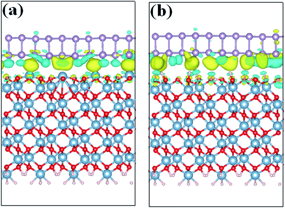 | ||
| Fig. 2 Charge density differences for BP adsorbed on (a) Al-terminated, and (b) fully hydroxylated Al2O3 (0001) surfaces. Blue (yellow) regions show electron accumulation (depletion). | ||
We now turn to discussing the effects of an Al2O3 substrate on the electronic band structure of BP. The projected band structure of single-layer BP adsorbed on an Al-terminated surface (B1Al configuration) is shown in Fig. 3(a). We notice that the band gap nature of BP transforms from direct to indirect due to a shift in the conduction band minimum from the Γ point to the Χ point, and the band gap value is enlarged by ∼160 meV compared with isolated, free-standing BP (Fig. 3(c)). These band structure changes mainly result from inter-layer charge transfer. The charge-density distributions of the conduction-band minimum (CBM) and valence-band maximum (VBM) of BP on an Al-terminated Al2O3 surface (Fig. 3(d)) are found to be much more non-uniform compared with that of pure BP (Fig. 3(f)). For the hydroxylated case (B1O configuration), the band structure nature of BP is almost unchanged and only a negligible increase in the band gap of BP (∼84 meV) is observed in Fig. 3(b), indicating that hydroxylated Al2O3 preserves the intrinsic band structure of BP well, owing to weak vdW interactions. However, the rippled structure at the interface still makes the corresponding charge-density distributions of the CBM and VBM (Fig. 3(e)) more localized in different parts of the BP layer.
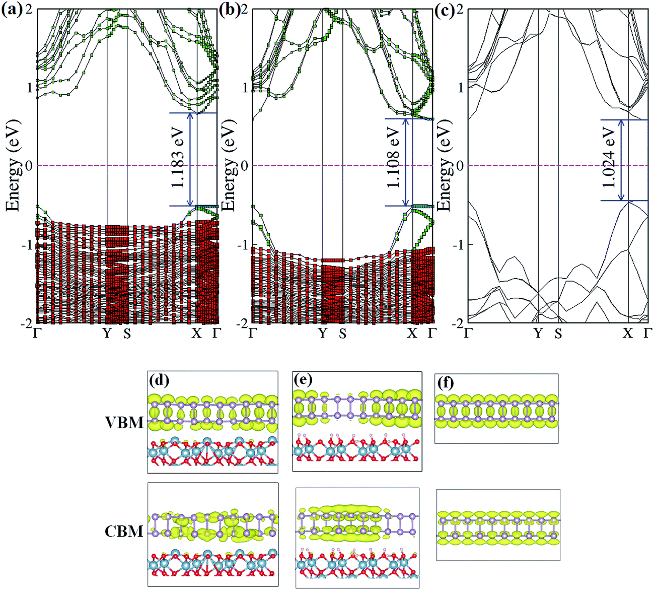 | ||
| Fig. 3 The band structure of BP adsorbed on (a) Al-terminated, and (b) fully hydroxylated Al2O3 surfaces, and (c) pure BP band structure. The green squares and red squares represent the band structure projected on BP and Al2O3, respectively. (d)–(f) Isosurfaces of the band-decomposed charge density of the valence band maximum and conduction band minimum. | ||
In addition to the most stable configurations, the electronic band natures of other high symmetry configurations of BP on Al-terminated (Fig. 4(a)–(d)) and hydroxylated (Fig. 4(e) and (f)) Al2O3 surfaces are examined and found to be close to those of B1Al or B1O. The differences in the band gap between the most stable configuration and other high symmetry configurations are no larger than 0.01 eV (0.015 eV) for BP on an Al-terminated (hydroxylated) Al2O3 surface, indicating that a similar on/off ratio could be obtained even if BP slides away from its ground state B1Al (B1O) configuration.
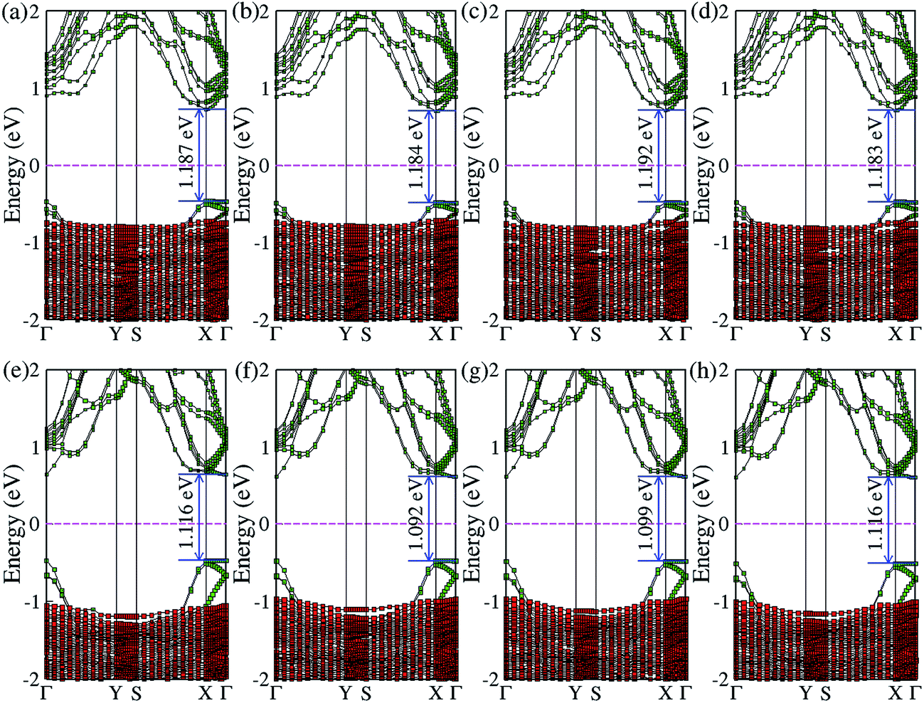 | ||
| Fig. 4 The band structures of other high symmetry configurations of BP on Al-terminated (a)–(d) and hydroxylated (e)–(h) Al2O3 surfaces. The green and red squares represent the band structure projected on BP and Al2O3, respectively. | ||
The band gaps of few-layer BP on Al-terminated and hydroxylated Al2O3 surfaces are shown in Fig. 5. It can be seen that the band gap of isolated BP decreases with an increasing number of layers, due to enhanced interlayer interactions, which is consistent with previous studies.38 We note that this trend does not change when placing few-layer BP on Al-terminated or hydroxylated Al2O3 surfaces. Interestingly, the band gaps, which are enlarged by the substrate effect in monolayer BP, gradually reduce upon increasing the number of layers in both the Al-terminated and hydroxylated case, compared with isolated BP layers. For example, the band gaps of monolayer BP on Al-terminated and hydroxylated surfaces are individually increased by 0.16 eV and 0.08 eV, while that of four-layer BP on the two surfaces are decreased by 0.07 eV and 0.02 eV, respectively, compared with isolated BP. After carefully examining the contents of the VBM and CBM of BP, it is found that both the VBM and CBM of free BP are composed of the pz orbitals of P atoms. As BP is placed on Al-terminated Al2O3, the pz orbitals in the VBM are hardly affected by interlayer interactions, but those in the CBM are suppressed, and its energy is largely increased, leading to a new CBM arising and the band gap of BP enlarging. However, for few-layer BP, the interlayer interactions have little influence on the CBM and the decreased band gaps are mainly due to interlayer charge transfer. Furthermore, the band gap reduction for few-layer BP on an Al-terminated Al2O3 surface is larger than on the hydroxylated Al2O3 surface, due to stronger interactions between the BP and Al-terminated Al2O3 surface. Moreover, it is worth mentioning that the band gap of bilayer BP is nearly independent of the substrate, indicating that it may be a potential candidate for special device applications.
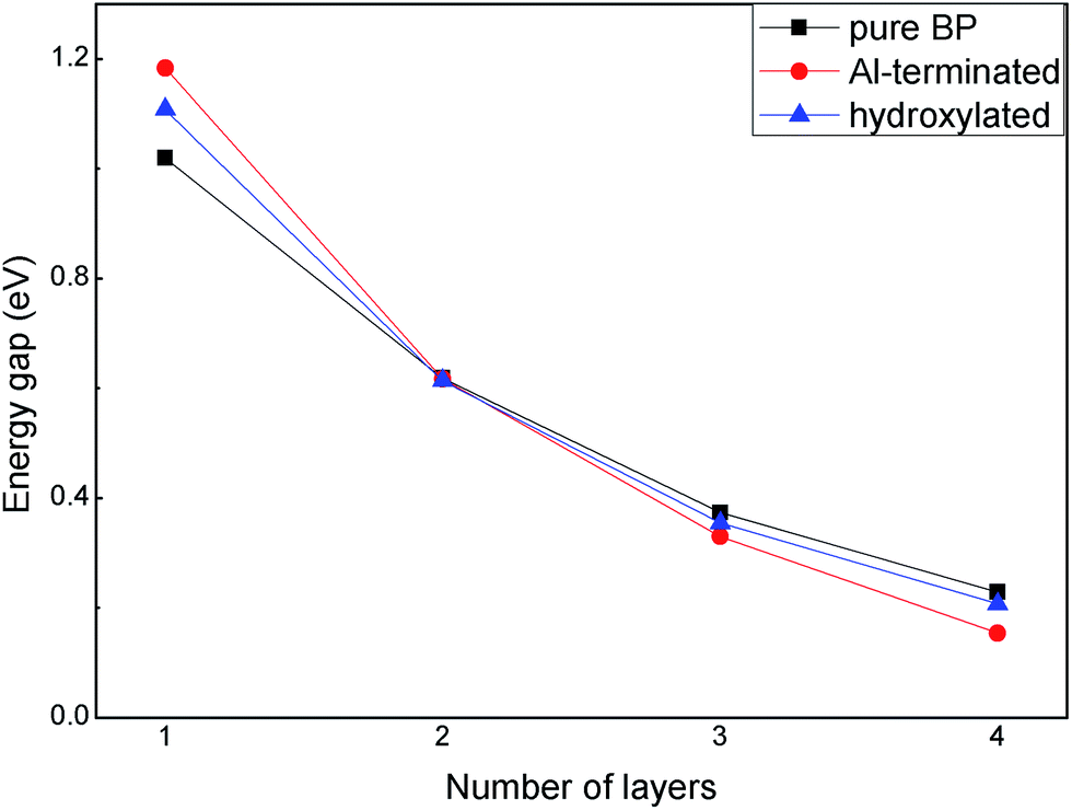 | ||
| Fig. 5 The band gaps of few-layer BP adsorbed on Al-terminated and hydroxylated Al2O3 surfaces. | ||
In comparison with band structures, the band offset of semiconducting heterostructures is also very important in material and device design.39 Precise knowledge is extremely important to engineer electronic and optoelectronic devices. The band alignments of a BP/Al2O3 system have been calculated using the macroscopic averaging method.40 The electrostatic potential has been chosen as a reference, the change in the average electrostatic potential through the interface is obtained through calculating the BP/Al2O3 heterostructures, and the VBMs of the two semiconductors with respect to the electrostatic potential have been calculated using their individual supercells. The calculated results in Fig. 6 show that the macroscopic average potential is discontinuous at the interface of BP and Al2O3, indicating that electrons should overcome a potential barrier (3.5–3.8 eV) to cross from Al2O3 to the BP section. We note that the VBM of BP is higher than that of Al2O3, which indicates that BP and Al-terminated Al2O3 form a type I heterointerface, due to a large band gap in bulk Al2O3 (our DFT + PBE result is 6.2 eV). The predicted valence-band offset (VBO) ΔEV between monolayer BP and Al2O3 is about 0.4 eV (Fig. 6(a)), which is smaller than that of graphene/Al2O3 and MoS2/Al2O3. This value may not be ideal for practical FET devices based on BP material. For practical use, the valence band offset is expected to be sufficiently large (>1.0 eV), which allows suppression of electron thermal emission from channel to the gate or reduction of the gate leakage current. As the number of BP layers increases, the VBO of few-layer BP is enlarged, but not monotonic. The VBO values are 1.32, 0.96 and 1.15 eV for bilayer, three-layer and four-layer BP, respectively (Fig. 6(b)–(d)), which is more appropriate for creating a reasonable carrier injection barrier.
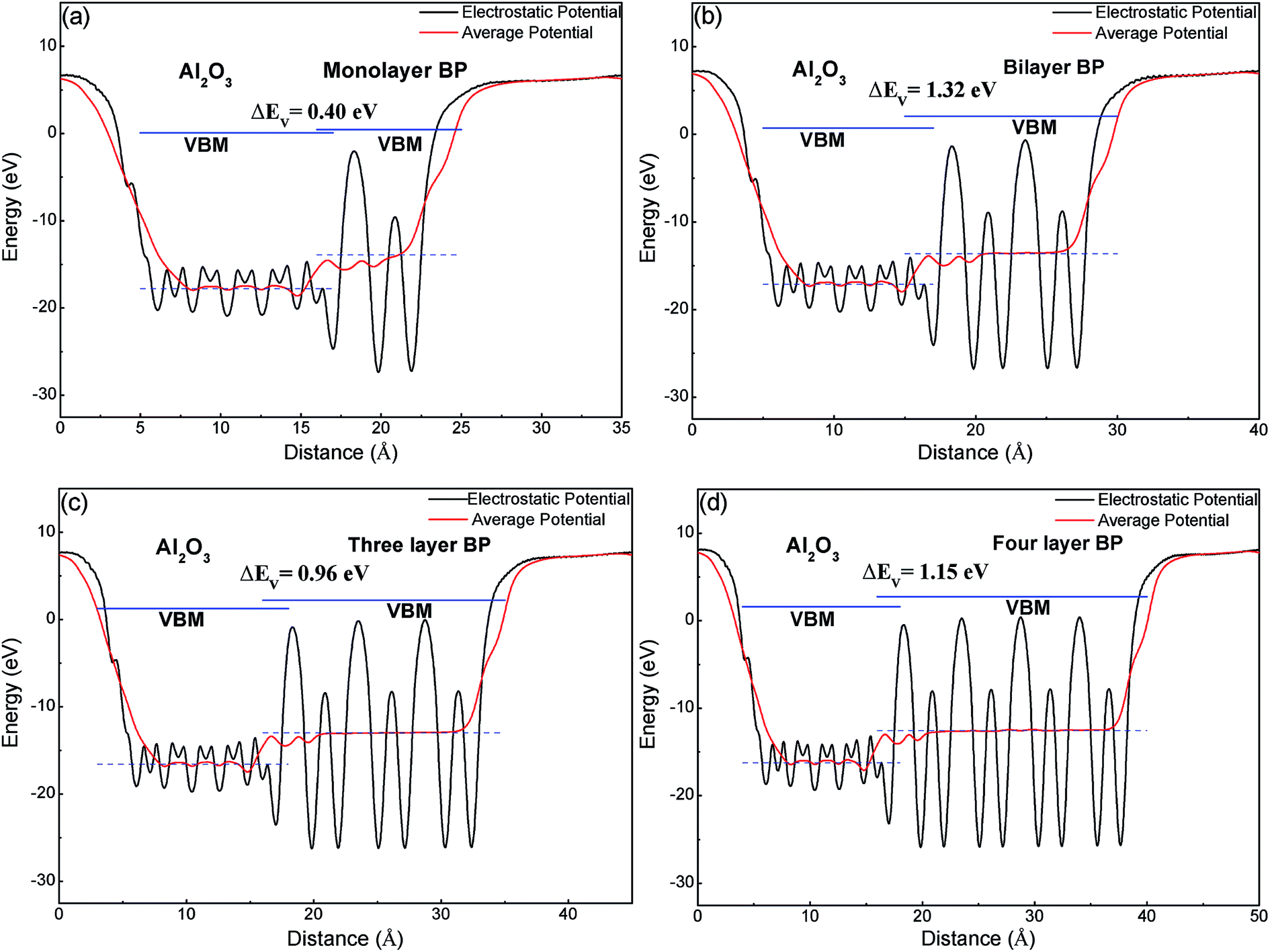 | ||
| Fig. 6 The band alignment of (a) monolayer, (b) bilayer, (c) three layer, (d) four layer BP adsorbed on an Al-terminated Al2O3 surface. | ||
Finally, we considered the electronic properties of a BP/Al2O3 hybrid system under an external electric field (Eext) to simulate the gating effect in experiments. Fig. 7 shows the band gaps of BP/Al2O3 systems as a function of Eext. The positive (negative) values of Eext represent the direction of Eext vertical to the BP plane and pointing from Al2O3 (BP) to BP (Al2O3). For monolayer BP on an Al-terminated Al2O3 surface, the band gaps show negligible changes under a negative Eext; this trend is destroyed under a positive Eext, as Eext > 0.3 V Å−1, which decreases the band gap. The band gap variations for monolayer BP on a hydroxylated Al2O3 surface undergo a similar trend as for the Al-terminated case. However, they seem more sensitive to Eext, with a larger reduction in band gap found as Eext > 0.3 V Å−1. For example, the band gap in the hydroxylated case decreases by about 0.34 eV under Eext = 0.6 V Å−1, while that value for the Al-terminated case is only 0.14 eV under the same Eext. This is mainly because the distance between the monolayer BP and hydroxylated Al2O3 surface is more severely decreased compared to that for an Al-terminated surface under Eext = 0.6 V Å−1, due to the relatively weak vdW interactions. We have checked that the reduction distances are 0.34 Å and 0.14 Å for the hydroxylated and Al-terminated case under Eext = 0.6 V Å−1, respectively. The changed interlayer distance will cause interlayer charge transfer and redistribution, thus changing the band gap. The situation is quite different for bilayer BP/Al2O3, in which case we note that the band gaps of BP on Al-terminated and hydroxylated Al2O3 surfaces under a negative Eext are nearly the same, both monotonically decreasing upon an increasing Eext value. Under a positive Eext, the band-gap variations for BP on an Al-terminated Al2O3 surface show an increasing and then decreasing trend. For BP on a hydroxylated Al2O3 surface, the band-gap modulations are analogous to those under a negative Eext, decreasing but with a more smooth trend. Therefore, the electronic properties of BP rely on the substrate interface, as modulated by the external electric field. Though the non-bonding model of the BP/Al2O3 hybrid system in our work is not precise enough for a thorough description of the interactions between BP and the Al2O3 surface under practical experiment, which may include defects, adsorbates, oxides in the interface and the formation of bond states, it still gives useful information on how the electronic properties of the BP layer are affected by an Al2O3 dielectric, which we think may contribute to practical device design.
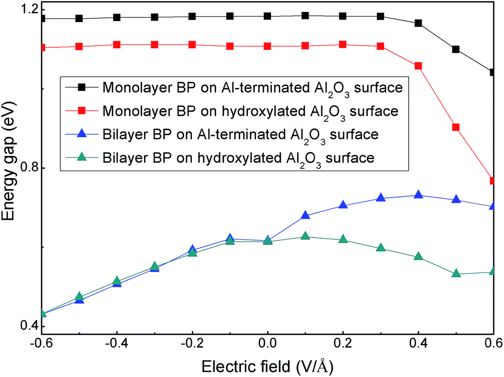 | ||
| Fig. 7 The band gaps of monolayer and bilayer BP adsorbed on Al-terminated and hydroxylated Al2O3 surfaces as a function of external electric field. | ||
Conclusions
In summary, first principles calculations have been performed to systematically study the electronic properties of BP on Al-terminated and hydroxylated Al2O3 surfaces. We found that the Al-terminated Al2O3 surface would induce a shift of the conduction band minimum of BP, while a hydroxylated Al2O3 surface could maintain well the intrinsic band nature of BP. The band gaps of BP on the two surfaces are both enlarged, due to interlayer charge transfer between BP and Al2O3. However, the band gaps of few-layer BP (2–4 layers) were decreased compared with isolated BP in both the Al-terminated and hydroxylated case. The band offset of a monolayer BP/Al2O3 system was predicted to be 0.4 eV, which was probably not ideal for practical FET devices, however, increased band offsets were found in few-layer BP, making it more suitable for creating an injection barrier. Moreover, the band gaps of a BP/Al2O3 system could be modulated using an external electric field for practical applications.Acknowledgements
We acknowledge the National Nature Science Foundation of China (Grant No. 21573129 and 21403300), the National Nature Science Foundation of Shandong Province (Grant No. ZR2015BQ001), and the General Financial Grant from the China Postdoctoral Science Foundation (Grant No. 2013M531595). The authors also acknowledge a generous grant of computer time from the National Supercomputer Center in Tianjin-TianHe-1(A) and the Norwegian Programme for Supercomputing.References
- L. K. Li, Y. J. Yu, G. J. Ye, Q. Q. Ge, X. D. Ou, H. Wu, D. L. Feng, X. H. Chen and Y. B. Zhang, Nat. Nanotechnol., 2014, 9, 372–377 CrossRef CAS PubMed.
- Y. C. Du, H. Liu, Y. X. Deng and P. D. Ye, ACS Nano, 2014, 8, 10035–10042 CrossRef CAS PubMed.
- H. Liu, A. T. Neal, Z. Zhu, Z. Luo, X. F. Xu, D. Tománek and P. D. Ye, ACS Nano, 2014, 8, 4033–4041 CrossRef CAS PubMed.
- K. S. Novoselov, A. K. Geim, S. V. Morozov, D. Jiang, Y. Zhang, S. V. Dubonos, I. V. Grigorieva and A. A. Firsov, Science, 2004, 306, 666–669 CrossRef CAS PubMed.
- B. Radisavljevic, A. Radenovic, J. Brivio, V. Giacometti and A. Kis, Nat. Nanotechnol., 2011, 6, 147–150 CrossRef CAS PubMed.
- M. Buscema, D. J. Groenendijk, S. I. Blanter, G. A. Steele, H. S. J. van der Zant and A. Castellanos-Gomez, Nano Lett., 2014, 14, 3347–3352 CrossRef CAS PubMed.
- S. Zhang, J. Yang, R. J. Xu, F. Wang, W. F. Li, M. Ghufran, Y. W. Zhang, Z. F. Yu, G. Zhang, Q. H. Qin and Y. R. Lu, ACS Nano, 2014, 8, 9590–9596 CrossRef CAS PubMed.
- V. Tran, R. Soklaski, Y. F. Liang and L. Yang, Phys. Rev. B: Condens. Matter Mater. Phys., 2014, 89, 235319 CrossRef.
- S. J. Yuan, A. N. Rudenko and M. I. Katsnelson, Phys. Rev. B: Condens. Matter Mater. Phys., 2015, 91, 115436 CrossRef.
- V. Wang, Y. Kawazoe and W. T. Geng, Phys. Rev. B: Condens. Matter Mater. Phys., 2015, 91, 045433 CrossRef.
- D. Xiang, C. Han, J. Wu, S. Zhong, Y. Y. Liu, J. D. Lin, X. A. Zhang, W. P. Hu, B. Özyilmaz, A. H. Castro Neto, A. T. S. Wee and W. Chen, Nat. Commun., 2015, 6, 6458 CrossRef PubMed.
- D. J. Perello, S. H. chae, S. Song and Y. H. Lee, Nat. Commun., 2015, 6, 7809 CrossRef CAS PubMed.
- J. O. Island, G. A. Steele, H. S. J. van der Zant and A. Castellanos-Gomez, 2D Mater., 2015, 2, 011002 CrossRef.
- P. Li, D. Z. Zhang, J. J. Liu, H. Y. Chang, Y. E. Sun and N. L. Yin, ACS Appl. Mater. Interfaces, 2015, 7, 24396–24402 CAS.
- S. P. Koenig, R. A. Doganov, H. Schmidt, A. H. Castro Neto and B. Özyilmaz, Appl. Phys. Lett., 2014, 104, 103106 CrossRef.
- J. D. Wood, S. A. Wells, D. Jariwala, K. S. Chen, E. K. Cho, V. K. Sangwan, X. L. Liu, L. J. Lauhon, T. J. Marks and M. C. Hersam, Nano Lett., 2014, 14, 6964–6970 CrossRef CAS PubMed.
- A. Javey, H. Kim, M. Brink, Q. Wang, A. Ural, J. Guo, P. McIntyre, P. McEuen, M. Lundstrom and H. J. Dai, Nat. Mater., 2002, 1, 241–246 CrossRef CAS PubMed.
- V. K. Sangwan, D. Jariwala, K. Everaerts, J. J. McMorrow, J. T. He, M. Grayson, L. J. aluhon, T. J. Marks and M. C. Hersam, Appl. Phys. Lett., 2014, 104, 083503 CrossRef.
- S. Kim, J. Nah, I. Jo, D. Shahrjerdi, L. Colombo, Z. Yao, E. Tutuc and S. K. Banerjee, Appl. Phys. Lett., 2009, 94, 062107 CrossRef.
- R. A. Doganov, S. P. Koenig, Y. Yeo, K. Watanabe, T. Taniguchi and B. Özyilmaz, Appl. Phys. Lett., 2015, 106, 083505 CrossRef.
- B. Huang, Q. Xu and S. H. Wei, Phys. Rev. B: Condens. Matter Mater. Phys., 2011, 84, 155406 CrossRef.
- A. K. Singh, R. G. Henig, A. V. Davydov and F. Tavazza, Appl. Phys. Lett., 2015, 107, 053106 CrossRef.
- H. Liu, A. T. Neal, M. W. Si, Y. C. Du and P. D. Ye, IEEE Electron Device Lett., 2014, 35, 795–797 CrossRef CAS.
- X. Luo, Y. Rahbarihagh, J. C. M. Hwang, H. Liu, Y. C. Du and P. D. Ye, IEEE Electron Device Lett., 2014, 35, 1314–1316 CrossRef.
- Y. Q. Cai, G. Zhang and Y. W. Zhang, J. Phys. Chem. C, 2015, 119, 13929–13936 CAS.
- L. Shao, H. G. Ye, Y. L. Wu, Y. X. Du, P. Ding, F. G. Zeng and Q. X. Yuan, Mater. Res. Express, 2016, 3, 025013 CrossRef.
- P. J. Eng, T. P. Trainor, G. E. Brown Jr, G. A. Waychunas, M. Newville, S. R. Sutton and M. L. Rivers, Science, 2000, 288, 1029–1033 CrossRef CAS PubMed.
- G. Kresse and J. Hafner, Phys. Rev. B: Condens. Matter Mater. Phys., 1993, 47, 558–561 CrossRef CAS.
- J. P. Perdew, K. Bruke and M. Ernzerhof, Phys. Rev. Lett., 1996, 77, 3865–3868 CrossRef CAS PubMed.
- S. Grimme, Comput. Chem., 2006, 27, 1787–1799 CrossRef CAS PubMed.
- J. Ahn and J. W. Rabalais, Surf. Sci., 1997, 388, 121–131 CrossRef CAS.
- P. Guénard, G. Renaud, A. Barbier and M. Gautier-Soye, Surf. Rev. Lett., 1998, 05, 321 CrossRef.
- M. Gautier, G. Fenaud, L. P. Van, B. Villette, M. Pollak, N. Thromat, F. Jollet and J. P. Duraud, J. Am. Ceram. Soc., 1994, 77, 323–334 CrossRef CAS.
- R. D. Felice and J. E. Northrup, Phys. Rev. B: Condens. Matter Mater. Phys., 1999, 60, 16287 CrossRef.
- X. G. Wang, A. Chaka and M. Scheffler, Phys. Rev. Lett., 2000, 84, 3650–3653 CrossRef CAS PubMed.
- Y. J. Kang, J. Kang and K. J. Chang, Phys. Rev. B: Condens. Matter Mater. Phys., 2008, 78, 115404 CrossRef.
- E. Sanville, S. D. Kenny, R. Smith and G. Henkelman, J. Comput. Chem., 2007, 28, 899–908 CrossRef CAS PubMed.
- J. S. Qiao, X. H. Kong, Z. X. Hu, F. Yang and W. Ji, Nat. Commun., 2014, 5, 4475 CAS.
- A. Franciosi and C. G. Van de Walle, Surf. Sci. Rep., 1996, 25, 1–140 CrossRef CAS.
- A. Baldereschi, S. Baroni and R. Resta, Phys. Rev. Lett., 1988, 61, 734–737 CrossRef CAS PubMed.
| This journal is © The Royal Society of Chemistry 2017 |