
 Open Access Article
 This Open Access Article is licensed under a
 Creative Commons Attribution 3.0 Unported Licence
Low-cost nanocarbon electrodes on arbitrary fibrous substrates as efficient bifacial photovoltaic wires
Wen Liua,
Ming Pengbc,
Si Chenb,
Dechun Zou*b,
Chaoqun Zhanga,
Yueping Fanga and
Xin Cai *ab
*ab
aCollege of Materials and Energy, South China Agricultural University, Guangzhou, Guangdong 510642, China. E-mail: caixin2015@scau.edu.cn
bBeijing National Laboratory for Molecular Sciences, Key Laboratory of Polymer Chemistry and Physics of Ministry of Education, College of Chemistry and Molecular Engineering, Peking University, Beijing 100871, China
cWuhan Institute for Food and Cosmetic Control, Wuhan 430012, China
First published on 1st February 2017
Abstract
The emergence of wearable electronics has demanded advances in efficient flexible/wearable energy devices. Photovoltaic wires (PVWs) have unique 3D light-harvesting capabilities and available electrode materials that are attractive for this purpose. Developing low-cost and efficient Pt-free fibrous counter electrodes (CEs) for PVWs is essential. Herein, ultralow-cost nanocarbon, with considerable electrochemical activity, was deposited onto arbitrary fibers, including TiO2 semiconductor, metal wires, and polymeric carbon fibers, using a facile dip-coating method. These fibers were then used as efficient catalytic fibrous CEs in PVWs. The influence of nanocarbon loading and charge transfer resistance on electrocatalytic activity were investigated in nanocarbon-penetrated Ti/TiO2 nanotube array CEs and dummy cells based on SS wire/nanocarbon CEs. Due to the balanced influences of conductive substrate and nanocarbon electrocatalytic film, PVWs assembled from SS wire/nanocarbon CE and an all-carbon carbon fiber/nanocarbon CE achieved efficiencies of 6.09% and 5.10% under AM1.5G illumination (100 mW cm−2), respectively. Furthermore, a double-sided illuminated PVW had an apparent efficiency of 10.8%. This work demonstrates innovative cost-efficient photovoltaic wires that may help boost low-cost, bifacial and highly flexible/wearable photovoltaics toward practical applications.
Introduction
Smart electronics, now considered an indispensable part of convenient and easy living in modern society, are increasingly popular and have rapidly progressed in recent years. Electronic devices that can be worn on the wrist, neck, ears, or clothes are emerging, and are expected to initiate a new technological revolution in our daily lives.1 To function, wearable electronic devices must have efficient and suitable power supply units. Nowadays, many researchers are dedicated to developing miniaturized, high-performance flexible/wearable energy devices for portable power supplies and wearable electronics.2,3 Flexible/wearable energy devices are typically constructed on 2D substrates, such as metal sheets, plastics, and conducting carbon substrates (including carbon cloth, free standing carbon nanotube film, graphene films, and even paper), using modified processing for rigid electronics, or unique film processing techniques.4,5 However, if the 2D planar-format device is further simplified to a 1D wire-format, flexible wire-type devices that can be sewn, woven and knotted, and, hence, worn more easily, could be produced. Therefore, fiber electronics, including fiber logic circuits,6,7 fiber memory devices,8 fiber OLEDs,9 and fiber energy devices (including nanogenerators, photovoltaics, lithium ion batteries, and supercapacitors)10–13 have been reported, showing great potential for achieving multifunctional “smart fabrics” or “e-textiles”. With persistent research into efficient energy utilization, state-of-the-art fiber energy devices have been representative of flexible/wearable energy devices.14 However, the reported performances and large-scale production are still far from being used in practical applications.Photovoltaic wire or fiber (PVW or PVF) is an important emerging fiber energy device that can convert solar light to electricity. Unlike traditional planar sandwich-structured photovoltaics, PVWs can be divided into coaxial fiber structures and two-fiber structures (twisted or parallel). The latter usually leads to higher efficiency and easier processing.20 PVWs based on silicon film,15 organic/polymer active materials,16,17 ruthenium dyes18 and lead halide perovskites19 have been developed, among which state-of-the-art dye-sensitized photovoltaic (DSPV) fibers are still some of the most efficient, durable, and technically accessible examples. Typically, DSPVW uses Pt wire as the counter electrode (CE) to ensure efficient photoelectric conversion. However, precious platinum is expensive and scarce, limiting the wide application of PVWs. Therefore, Pt-free CEs for efficient PVWs are of great interest.
An ideal strategy for produce efficient fibrous Pt-free CEs involves developing novel fibers that are electrically conductive, tough, and electrochemically activity. Taking advantage of nanofabrication technologies, spun carbon nanotube fibers, and graphene fibers were demonstrated as feasible CEs for PVWs.21,22 Regardless of the relatively complicated process used to achieve low dimensional nanocarbon-based macroscopic fibers with the required properties, Pt nanoparticles are still involved in CEs, resulting in PVWs with desirable efficiencies.23 An alternative strategy is the deposition of electroactive materials onto conductive metal wires, conductive polymer fibers, or insulating yarns. Carbon nanotube films, reduced oxide graphenes, PEDOT conducting polymer, and various metallic compounds, such as TiN nanoplates, and Co2Ni2S4 nanoribbons and nanocomposites, have been prepared on metal wires or carbon fibers (CFs),24–28 and gave efficiencies of 5–7% as DSPVWs. Investigating appropriate film preparation on nonplanar fibrous substrates, and the rational design of electrocatalytic nanomaterials with enough active sites and proper porous morphology, are crucial.29 Despite this progress, continuing efforts are needed to develop more cost-efficient fibrous CEs. Furthermore, the influence of the substrate material and electrocatalytic film in fibrous CEs should be examined and balanced for long-term applications.
Herein, ink nanocarbon (NC), a common nanocarbon material, was directly used as an electrocatalytic material for PVWs. Owing to its ultralow cost, high dispersion stability, and unique accessibility, ink NC composed of graphitic carbon black particles is an attractive material for fabricating efficient photovoltaic cells on various substrate materials, using printing, spin-coating, dip-coating, or other techniques. In this work, NC was chosen as the electrocatalyst for building PVWs on different substrates, including Ti wire, stainless steel (SS) wire, and CFs. Using the anodization of titanium wire to grow oriented TiO2 nanotube (TNT) arrays, NC-penetrated Ti/TNT CE was prepared and studied for PVWs. The effects of NC loading, charge transport, and electrolyte diffusion on the catalytic activity of the fibrous CEs were investigated. PVWs based on a NC-coated SS wire CE and CF CE demonstrated a power conversion efficiency of 6.09% and 5.10%, respectively, making them among the most cost-efficient PVWs.
Experimental section
1. Preparation of Ti-wire-based TiO2 photoanode
Titanium wires (99.7%, φ = 0.25 mm, Alfa Aesar) were cleaned by ultrasonicating in acetone, isopropanol, and ethanol for 20 min each. TiO2 colloids were prepared using a previously reported method.30 To obtain TiO2-film-coated Ti-based photoanodes, the cleaned Ti wires were first heated at 350 °C on a hotplate for 10 min, during which the surface changed from grey-white to a brownish yellow. The Ti wires were then dipped into TiO2 colloids, removed, and heated on a hot plate to remove solvent. This dip-coating process was repeated several times until the desired TiO2 film thickness was achieved. Notably, the thickness of the TiO2 film was easily controlled by adjusting the dip-coating time and the TiO2 colloid concentration. The TiO2-coated Ti wires were annealed at 450 °C under air for 30 min, cooled to about 100 °C, and then immersed in a 0.5 mM solution of N719 dye (Dalian Heptachroma, China) in ethanol overnight. Finally, the dye-sensitized Ti/TiO2 electrodes were rinsed with anhydrous ethanol to remove unadsorbed dye molecules, affording the Ti-wire-based TiO2 photoanodes.2. Preparation of fibrous counter electrode (CE)
Nanocarbon dispersion (Hero, Shanghai Ink Factory, China) was used as received.3. Device assembly
All photovoltaic devices in this study were assembled using a parallel structure, with the fibrous Ti-wire-based TiO2 photoanode placed parallel to another fibrous CE (Ti/TNT/NC, SS wire/NC, or CF/NC). It should be noted that Pt wire (φ = 80 μm) can be used directly as the standard CE for comparison. Both the photoanode and CE were inserted into a capillary (φinner = 0.9–1.1 mm) filled with an iodine electrolyte composed of 1-butyl-3-methylimidazolium iodide (BMII; 0.6 M), iodine (I2; 0.03 M), 4-tert-butylpyridine (TBP; 0.3 M), lithium perchlorate (LiClO4; 0.05 M), and guanidine thiocyanate (GuSCN; 0.05 M) in acetonitrile. Dummy cells were assembled using two identical SS wire/NC CEs prepared under the same conditions. Melted wax was used to seal both ends of the capillary to finish the devices.4. Methods and characterization
In situ X-ray diffraction (XRD) patterns were recorded on an X-ray diffractometer (Bruker, D8 Advance). Nitrogen adsorption–desorption isotherm plots of NC annealed at 350 °C were measured using an ASAP 2010 Micrometer at 77 K. The microstructure and film morphology of the electrodes were imaged using field emission scanning electron microscopy (FESEM, S-4800 Hitachi). The current–voltage (I–V) characteristics of the photovoltaic wires were analyzed using a Keithley Model 2000 multimeter equipped with a simulated solar lamp (Yamashita DESO, Japan). Unless specified, the light intensity was calibrated at 100 mW cm−2 (AM1.5G illumination) using a silicon solar cell. Typically, the effective aperture area of the photovoltaic wire was calculated from the projected area (Ap), which was equal to the device length multiplied by the apparent photoanode diameter.16,18–20,31 Electrochemical impedance spectroscopy (EIS) of the photovoltaic wires and dummy cells was conducted using PGSTAT302N (Autolab Corp., Switzerland) with a perturbation voltage of 10 mV under dark conditions. Different biases, from 0 to 0.8 V, could be applied to the device. The EIS frequency range was 100 kHz to 0.05 Hz. Cyclic voltammetry (CV) was carried out using a three-electrode setup, employing Pt as the CE, AgCl/Ag as the reference electrode, and SS wire/NC, CF/NC, or Pt wire (φ = 80 μm) as the working electrode. The potential scanning rate ranged from 10 to 250 mV s−1 and an acetonitrile electrolyte containing BMII (10 mM), I2 (1 mM), and LiClO4 (0.05 M) was used.Results and discussion
Before deposition of the electrocatalytic NC film, Ti electrolysis was performed to grow TNT film on the fibrous Ti substrate, which increased the surface loading capacity for electroactive materials on the metal support (Fig. 1a). Anodization of titanium metal is a facile and efficient way to prepare TNTs,32 and was applied to Ti wire in this study. Without polishing, the Ti wire surface was rough, as shown in Fig. 1b. After anodization, vertically aligned TNTs were grown in situ on Ti wire, as shown in Fig. 1c–h. To overcome significant surface tension caused by the cylindrical Ti substrate during TNT growth, several long and narrow cracks formed along the fiber axis, as shown in Fig. 1c and e. The TNTs were found to grow in an almost open porous structure (Fig. 1d), which would benefit the deposition of targeted active substances. As demonstrated in Fig. 1f and g, the obtained TNTs had uniform diameters and orientations. Furthermore, the TNT film was in close contact with the Ti substrate, which would help reduce interface ohmic resistance in the Ti wire electrode (Fig. 1h). Fig. 2a shows the XRD patterns of annealed TNTs (denoted Ti/TNT). The diffraction peaks were easily attributed to the crystal planes of tetragonal anatase TiO2 (JCPDS 21-1272). Some weak peaks (marked with an asterisk in Fig. 2a) were visible for the Ti substrate due to the in situ measurement of XRD characteristics.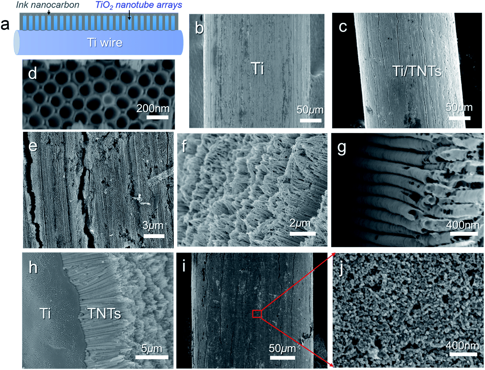 | ||
| Fig. 1 (a) Schematic diagram of ink NC-penetrated TiO2 nanotube arrays; (b) SEM image of Ti wire; (c)–(g) SEM top view images of TNTs by anodizing Ti wire; (h) TNT arrays vertically grown on Ti substrate; (i) SEM image of NC coated Ti/TNTs; and (j) SEM image of the NC film. | ||
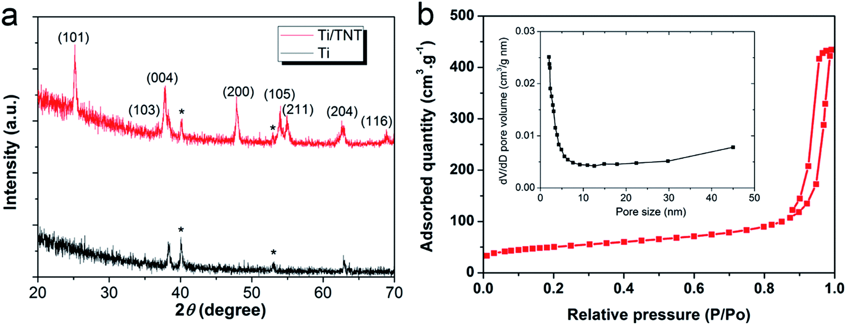 | ||
| Fig. 2 (a) XRD patterns of Ti wire substrate (Ti) and Ti/TiO2 nanotube array (Ti/TNT) electrodes after annealing at 450 °C for 30 min, respectively. (b) N2 adsorption–desorption isotherms of NC (treated by annealing at 350 °C in air for 30 min) at 77 K. Inset: corresponding Barrett–Joyner–Halenda adsorption pore-size distribution. | ||
Anodized Ti wires surrounded with TNTs were further coated with NC film using a simple solution adsorption-sintering process to achieve electrocatalytic CEs. As shown in Fig. 1i, the NC film was relatively smooth and covered the entire surface of the Ti/TNT electrode. The NC film was porous and composed of nanoparticles with diameter of approx. 20 nm (Fig. 1j). N2 adsorption–desorption tests were conducted to determine the specific surface area and pore size distribution of the annealed NC film. In this case, the Brunauer–Emmett–Teller (BET) surface area was calculated as 177.49 m2 g−1, along with pores exhibiting an average size of 15.15 nm distributed mainly in the mesoporous region. This considerable specific surface area could help the Ti wire-based CEs achieve efficient electrocatalytic activity.33 Fig. 3 shows SEM images of NC-penetrated Ti/TNT CEs. The NC nanoparticles were not only deposited uniformly on the surface of TNTs (after 8.5 h anodization), but also effectively filled empty space (gaps) between the TNTs (Fig. 3a and b), demonstrating the excellent infiltration capacity of NC into TNTs. When longer TNTs (after 25 h anodization) were used, an NC capping layer formed on the top of the TNTs, demonstrating the enhanced loading capacity of longer TNT arrays. Notably, the NC particles penetrated the space inside individual TNTs, probably due to the strong adhesion of the NC dispersion and open TNT structure (Fig. 3c and d).
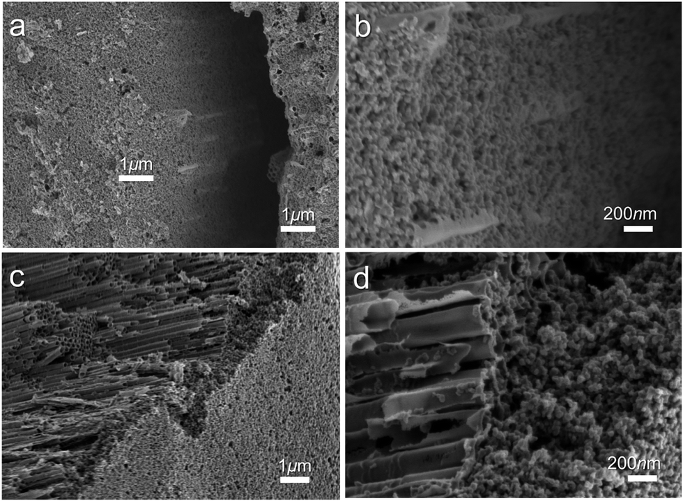 | ||
| Fig. 3 SEM images of NC-penetrated Ti/TNT CE after anodization for (a and b) 8.5 h and (c and d) 25 h. | ||
The above NC-penetrated Ti/TNT CE was further combined with a fibrous dye-sensitized TiO2 photoanode to prepare PVW, as illustrated in Fig. 4a and b. When light irradiates the photoanode side of the PVW, dye molecules generate photoelectrons that are then transmitted to the semiconductive TiO2 film and subsequently flow toward the external circuit through the Ti wire conductor. The electrons are then transported to the CE, and reduce I3− species in the electrolyte at the surface of the NC film, restoring the electrolyte composition and completing the photoelectrochemical cycle. An optical image of a typical PVW is shown in Fig. 4c. If the rigid capillary was simply replaced with a plastic encapsulation tube, the PVW would become highly flexible (Fig. 4d). To evaluate the influence of NC film and TNTs on device performance, PVWs were prepared from NC-penetrated TNT CEs with different anodization times. Fig. 5a and Table 1 show the corresponding CE photovoltaic performances. The photoelectric conversion efficiencies (η) of PVWs based on 0 h (PVW-0), 3.5 h (PVW-3.5), 8.5 h (PVW-8.5), 13.5 h (PVW-13.5), 20 h (PVW-20), and 25 h of anodization (PVW-25) were 3.63%, 1.65%, 1.71%, 2.50%, 2.71%, and 2.64%, respectively. As shown in Fig. 5b and c, the changes in open circuit voltage (Voc) and short-circuit current (Jsc) with increasing anodization time were insignificant. Therefore, it could be concluded that the variation in η was mainly affected by the fill factor (FF), which was largely dependent on the electrocatalytic activity of the adopted CE. PVW based on a Ti/NC electrode without TNTs gave the highest efficiency, while the introduction of TNTs deteriorated NC CE catalytic performance and, consequently, photoelectric conversion.
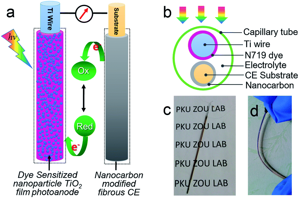 | ||
| Fig. 4 (a) Schematic illustration of PVW with Ti-wire-based photoanode and NC modified fibrous CE; (b) cross-sectional view of the PVW; (c) optical photograph of typical PVW (effective device length, approx. 5 cm) encapsulated in a glass capillary; and (d) optical photograph of a flexible PVW encapsulated with flexible and transparent plastic tube. | ||
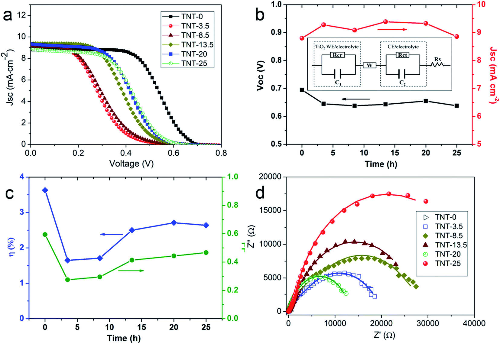 | ||
| Fig. 5 (a) I–V curves of PVWs based on NC-penetrated TNT CEs prepared using different anodization times; (b) variation in Voc and Jsc with anodization time (inset: equivalent circuit used for EIS fitting); (c) variation in η and FF with anodization time; and (d) Nyquist plots of PVWs based on NC-penetrated TNT CEs prepared using different anodization times. | ||
| Anodization time (h) | Voc (V) | Jsc (mA cm−2) | FF | Rs (Ω) | Rct (Ω) | η (%) |
|---|---|---|---|---|---|---|
| a Measurements were conducted with an applied bias of 0.65 V. | ||||||
| 0 | 0.695 | 8.80 | 0.594 | 4.85 | 4.11 | 3.63 |
| 3.5 | 0.645 | 9.28 | 0.275 | 6.52 | 1946 | 1.65 |
| 8.5 | 0.638 | 9.09 | 0.295 | 6.85 | 5428 | 1.71 |
| 13.5 | 0.643 | 9.39 | 0.414 | 6.41 | 1134 | 2.50 |
| 20 | 0.655 | 9.33 | 0.443 | 6.05 | 322.7 | 2.71 |
| 25 | 0.638 | 8.86 | 0.467 | 7.87 | 561.9 | 2.64 |
To further investigate the NC-penetrated Ti/TNT CE-based PVWs and the cause of performance degradation using TNTs, electrochemical impedance spectroscopy (EIS) analysis of the PVWs was conducted. According to the equivalent circuit (inset of Fig. 5b), Nyquist plots of the PVWs were obtained, as shown in Fig. 5d, and the corresponding Rs (series resistance) and Rct (charge transfer resistance at the CE–electrolyte interface) derived from the Nyquist plots are listed in Table 1. As the anodization time increased from 0 to 25 h, the resulting Rct sharply increased from 4.11 Ω for PVW-0 to 5428 Ω for PVW-8.5, followed by a remarkable drop to 322.7 Ω for PVW-20. Similarly, the Rs increased from 4.85 Ω to 6.85 Ω, and then decreased to 6.05 Ω for PVW-20. Generally, Rct was directly correlated with CE catalytic activity, while lower Rct values always facilitated electrochemical catalysis at the CE/electrolyte interface. This favored improved exchange current density and, therefore, good photovoltaic conversion performance.34 In this regard, the relatively low Rct originated from the benign catalytic activity of the NC film. Compared with the highly conducting Ti substrate, semiconductive TNTs would increase electrical resistance in the Ti electrode, in accordance with the slight increase in Rs. TNT arrays have been shown to accelerate carrier transport and collection in TiO2-based photoanodes because the ordered arrays aid electron diffusion and provide a more efficient charge transport path than random nanoparticles.35 However, this was not suitable to describe the NC-penetrated Ti/TNT CEs, as the Rct increased significantly, by 2–3 orders of magnitude. This implied that TNT arrays impeded charge transport in the CE instead of assisting the NC film with more efficient electron transport, which was likely to be associated with the photoinduced reaction and backward electron transfer in illuminated TNTs. This phenomenon should be the subject of continued research. Despite the adverse effects, TNT arrays can indeed serve as useful scaffolds to load more, or thicker, NC, which could achieved higher catalytic abilities and lower Rct values. This loading effective function was verified by the aforementioned capping layer present in longer TNTs after anodization for 25 h, but not in shorter TNTs (Fig. 3c and d). The inhibition effect and loading capacity had joint, but opposite, influences on Rct, in good agreement with the variations in Rct and η of the above PVWs. As a result, an optimal efficiency of 2.71% was achieved using PVW-20. However, as the TNTs were too long after 25 h of anodization, the inhibiting effect on charge transport played a dominant role and the photovoltaic performance of PVW-25 declined, in agreement with the IV results.
Based on the above analysis, it is worth noting that electrode conductivity, electrocatalytic film thickness, and intrinsic charge transport should be designed to guarantee desirable catalytic activity of the fibrous CEs. Therefore, SS wires were used to substitute for the Ti wire substrate. PVWs based on NC-coated SS wire CEs were fabricated with different film thicknesses and the corresponding photovoltaic performances are listed in Table 2. As shown in Fig. 6a, PVWs without NC coating showed almost no photoelectric conversion with a very low efficiency of 0.15%. The poor photovoltaic performance was further evidenced by the large Rct of 2.5 × 10⁵ Ω of the SS wire CE (Fig. 6b). When the NC film thickness was increased from 1.5 μm to 11 μm, the Voc and Jsc of the corresponding PVW was essentially maintained, while the FF increased gradually to 0.657. The best efficiency was obtained for PVWs based on SS wire/NC CE with a film thickness of 8 μm, while the photovoltaic performance of the PVW with a film thickness of 11 μm was only slightly lower. Likewise, Rct and Rs mainly influenced the trend in device performance, as described above (Fig. 6b). Usually, thicker NC film can enhance the catalytic surface area and favor the electrocatalytic ability of CE. Nevertheless, thicker NC film is less electrically conductive and would cause additional internal resistance in the CE, especially when the catalytic film is too thick for the efficient diffusion of electrolyte species. To better comprehend the influence of NC film thickness, dummy cells made from two identical SS wire/NC (1.5 μm) or SS wire/NC (8 μm) electrodes were prepared, denoted as DC-1.5 and DC-8, respectively. The EIS plots of DC-1.5 and DC-8 under different biases (0, 0.2 V, 0.4 V, 0.6 V, and 0.8 V) are presented in Fig. 6c and d. For DC-1.5, the semicircle in the mid-frequency range (1 kHz to 10 Hz) became two semicircles when the bias reached 0.4 V. With the bias exceeding 0.4 V, the two semicircles became more clear. This behavior could be elucidated from the diffusion impedance of electrolyte ions through the electrode pores giving rise to a bias-directed semicircle, which is relatively common in porous electroactive materials compared with bulk materials.36 For DC-8, the effect was even more significant because of the thicker NC film leading to aggravated diffusion impedance through the electrode pores. Other than the effect of catalytic film thickness on photovoltaic performance, the mechanical strength of the active electrode is important for practical applications. In our NC-based CEs, if the NC film was too thick, some NC particles might detach from the film because of the limited electrode strength, degrading the PVW photovoltaic performance, especially in devices under severe deformation or long term operation. Therefore, it was necessary to improve the electrocatalytic capability per unit thickness of the fibrous CE to achieve a truly high-performance electrode.
| Film thickness (μm) | Voc (V) | Jsc (mA cm−2) | FF | η (%) |
|---|---|---|---|---|
| 0 | 0.537 | 1.66 | 0.167 | 0.15 |
| 1.5 | 0.723 | 11.9 | 0.532 | 4.60 |
| 3 | 0.723 | 11.4 | 0.622 | 5.13 |
| 5 | 0.713 | 11.4 | 0.645 | 5.26 |
| 8 | 0.722 | 11.5 | 0.653 | 5.41 |
| 11 | 0.726 | 11.2 | 0.657 | 5.34 |
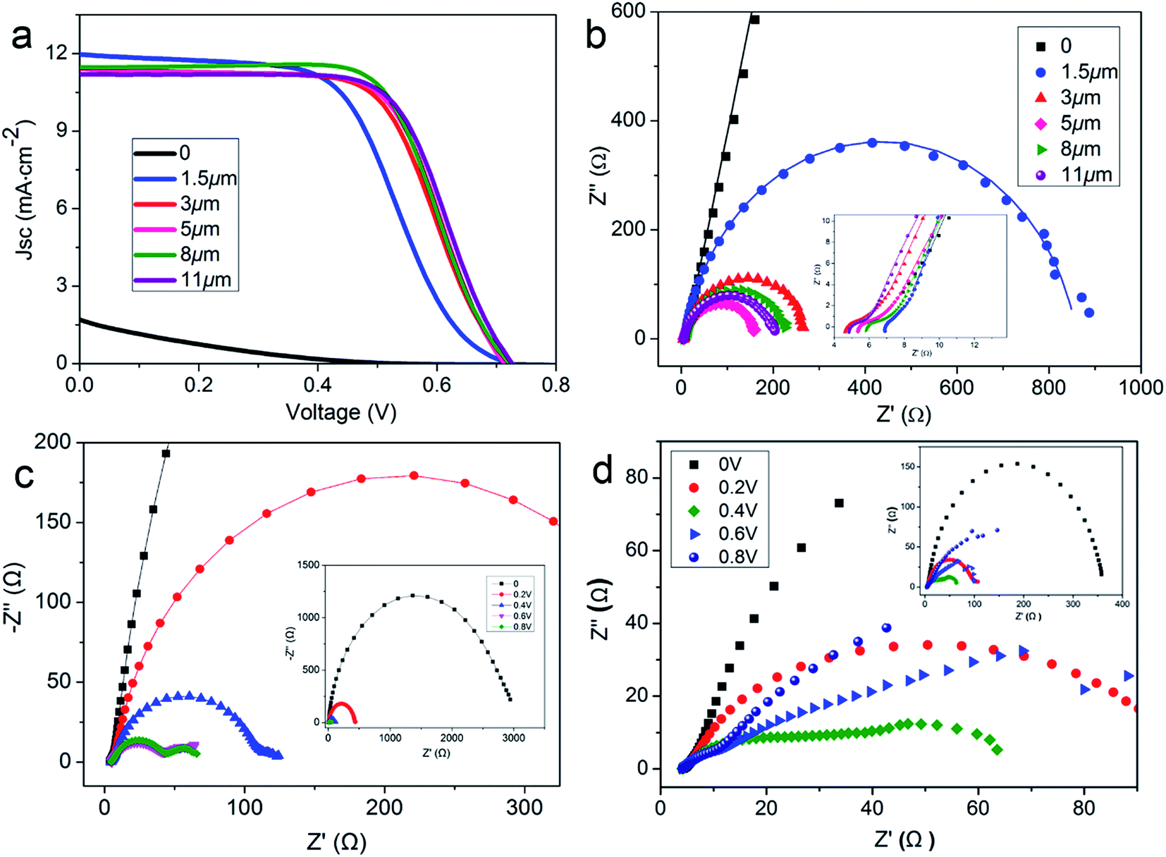 | ||
| Fig. 6 (a) I–V curves of PVWs based on SS wire/NC CEs with different film thicknesses, and Nyquist plots of (b) PVWs based on SS wire/NC CEs with different film thicknesses (inset: enlarged view of the high frequency region), (c) a dummy cell based on SS wire/NC CEs (NC film thickness, 1.5 μm) under different biases (inset: view of entire tested frequency region), and (d) a dummy cell based on SS wire/NC CEs (NC film thickness of 8 μm) under different biases (inset: view of entire tested frequency region). | ||
Furthermore, inexpensive CFs featuring macroscopic wire shapes, good availability, excellent mechanical properties, and considerable conductivity were directly applied to fibrous CEs. Fig. 7a–c show the SEM images of CF/NC electrodes. With simple dip-coating into an NC dispersion, a uniform NC shell was deposited onto the multiple CF cores, forming fibrous CF/NC electrodes with multi-core/shell structures. As shown in Fig. 7c, NC nanoparticles can effectively fill gaps between individual microfibers, which could greatly improve the catalytic surface of the CF/NC electrode. The catalytic activity of these fibrous CEs was further examined using CV characteristics. Fig. 7d–f show the CV curves of SS wire/NC, CF/NC, and Pt wire electrodes at different scanning rates. The pair of apparent redox peaks were easily assigned to the catalytic reactions of the I3−/I− couple. The dependence of the anodic (cathodic) peak current of catalytic oxidation (reduction) of iodide ions (triiodide ions) on the square root of scanning rate is derived in Fig. 7g. In particular, the anodic (cathodic) peak current of all three different electrodes had linear dependencies on the square root of the scanning rate, which inferred the diffusion-controlled catalytic dynamics of the electrode.37,38 Compared with Pt wire, the cathodic peak current of the SS wire/NC electrode had a slightly higher dependence on the scanning rate, resulting from additional diffusion impedance in the NC film, as stated in Fig. 6c and d. In the CF/NC electrode, much stronger dependence was observed, which explained the CF/NC electrode possessing the highest catalytic ability, associated with the most serious diffusion limitation, among the single CF/NC microelectrodes.
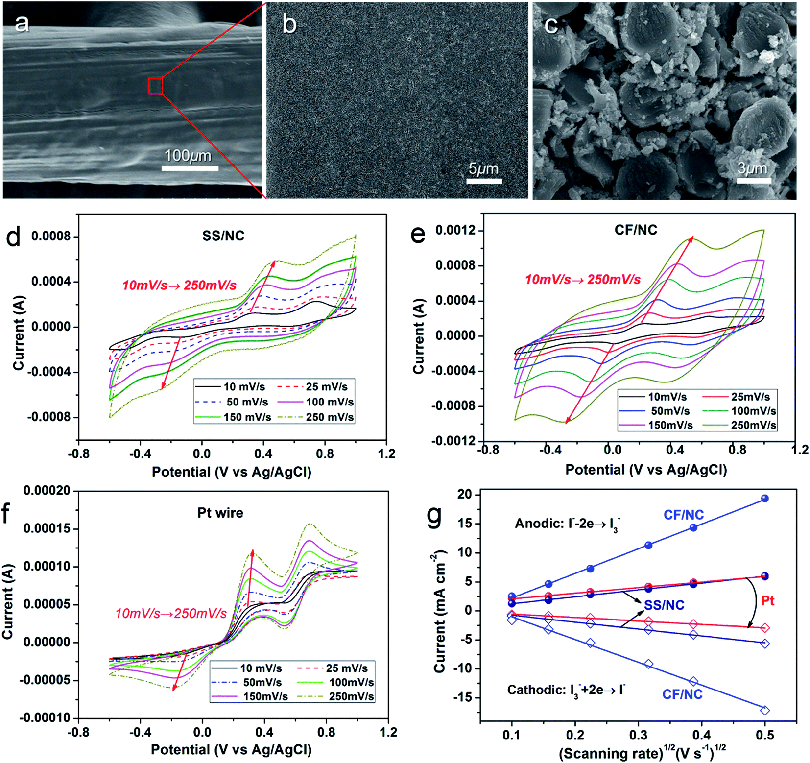 | ||
| Fig. 7 (a) SEM image of CF/NC electrode; (b) enlarged SEM image of NC film; (c) cross-sectional SEM image of CF/NC electrode. Cyclic voltammetry (CV) of (d) SS/NC, (e) CF/NC, (f) Pt wire electrode at different scanning rates; (g) the relationship between the redox current density and the scanning rate for SS/NC, CF/NC and Pt wire electrode, respectively. | ||
Eventually, preliminarily optimized PVWs based on Pt wire (D-Pt), CF/NC (D-CF), and SS wire/NC (D-SS) CEs were prepared and investigated, with the I–V curves displayed in Fig. 8. The Voc, Jsc, and FF of D-Pt were 0.751 V, 9.02 mA cm−2, and 0.702, respectively, giving rise to an η value of 4.76%. As for D-CF, the Voc, Jsc, and FF were 0.741 V, 9.35 mA cm−2 and 0.736, respectively, giving an η value of 5.10%. The improved photovoltaic performance of D-CF was mainly due to the superior catalytic ability of the CF/NC CE with multiple CF cores, which offered more NC loading sites and microfiber current collectors, in accordance with the CV results. Through collaborative optimization of the photoanode, the η value of D-SS reached 6.09%, with a Voc, Jsc, and FF of 0.633 V, 14.47 mA cm−2 and 0.665, respectively.
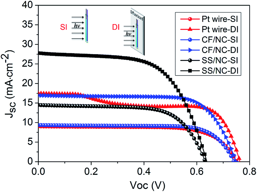 | ||
| Fig. 8 I–V curves of PVWs based on Pt wire, CF/NC, and SS wire/NC CEs. SI: standard illumination, AM1.5G, light intensity of 100 mW cm−2; DI: SI mode with a diffuse board at the bottom of the device. | ||
Considering the unique symmetry of the device architecture, a prominent advantage of PVWs over traditional planar-type photovoltaics is their outstanding 3D light harvesting capability. PVWs can capture reflected light, diffuse light, and stray light conveniently from all directions.16,20,39,40 When introducing a foam board as a diffuse reflector below the PVW, the photocurrent and photoelectrical output was greatly improved, and even doubled. For instance, D-Pt achieved an apparent efficiency of 8.64%. From Fig. 8, the anomalous change in the I–V curve for D-Pt in DI mode was caused by the restricted and insufficient electrocatalysis of Pt wire CE under concentrated intense light. For D-CF and D-SS with DI illumination, the apparent photoelectric conversion efficiency reached 9.09% and 10.8%, both representing a 1.8-fold, which was less than two-fold due to photon loss caused by the electrode shadow. In comparison with regular planar photovoltaic architectures, PVWs based on the above fibrous CEs are promising for developing low-cost, transparent, conductive, oxide-free, bifacial, and highly flexible/wearable photovoltaics using relatively simple processing. When compared with typical PVWs adopting a Pt wire CE, PVWs produced from both SS wire/NC CEs and CF/NC CEs exhibited better photoelectrical conversion performance. Furthermore, pen inks have been successfully used for more than 100 years. The NC-based electrodes produced herein were cheap and easy to prepare, owing to the low cost of commercial ink NC and its tolerance of a variety of substrate materials and film-processing methods. Interestingly, ultra-long flexible ink NC-based functional wires, with lengths exceeding several meters, can be produced and scaled-up by continuous “cup-to-cup” solution production.41 In particular, the all-carbon CF/NC fibrous CE was appealing for advancing lightweight, flexible and highly cost-efficient PVWs.
Conclusions
Using a facile and controlled dip-coating method, fibrous and Pt-free ink NC-penetrated Ti/TNTs, SS wire/NC, and CF/NC electrodes were prepared under mild conditions. The NC loading amount on the different substrate materials could be regulated by adjusting the anodization time to achieve in situ growth of ordered TiO2 nanotube arrays, film thicknesses, and multiple-carbon microfiber substrates. To achieve high performance PVWs, balancing the effect of NC loading on conductive fibers was key, taking into consideration the charge transport and electrolyte diffusion limitations in NC-based fibrous CEs. PVWs assembled from SS wire/NC CE exhibited the highest power conversion efficiency of more than 6%, with metal-free CF/NC CE expected to play a role in developing lightweight, bifacial, and flexible PVWs. Further investigations into electrolytes, such as replacing the liquid electrolyte with a gel or non-volatile ionic liquid, and device mechanical flexibility will help to develop even more efficient NC-based PVWs. Notably, NC-assembled PVWs could provide an alternative way to promote next-generation low-cost bifacial high performance flexible/wearable photovoltaics.Acknowledgements
This work was jointly supported by the Natural Science Foundation of China (NSFC 51602109, NSFC 91333107) and the Guangdong Provincial Science and Technology Project (No. 2016A050502048, No. 2014A030310427).References
- W. Weng, P. N. Chen, S. S. He, X. M. Sun and H. S. Peng, Angew. Chem., Int. Ed., 2016, 55, 6140–6169 CrossRef CAS PubMed.
- L. Li, Z. Wu, S. Yuan and X. B. Zhang, Energy Environ. Sci., 2014, 7, 2101–2122 CAS.
- X. Wang, X. Lu, B. Liu, D. Chen, Y. Tong and G. Shen, Adv. Mater., 2014, 26, 4763–4782 CrossRef CAS PubMed.
- H. C. Weerasinghe, F. Z. Huang and Y. B. Cheng, Nano Energy, 2013, 2, 174–189 CrossRef CAS.
- X. Cai, M. Peng, X. Yu, Y. P. Fu and D. C. Zou, J. Mater. Chem. C, 2014, 2, 1184–1200 RSC.
- M. Hamedi, R. Forchheimer and O. Inganas, Nat. Mater., 2007, 6, 357–362 CrossRef CAS PubMed.
- C. Muller, M. Hamedi, R. Karlsson, R. Jansson, R. Marcilla, M. Hedhammar and O. Inganas, Adv. Mater., 2011, 23, 898–901 CrossRef PubMed.
- G. Z. Sun, J. Q. Liu, L. X. Zheng, W. Huang and H. Zhang, Angew. Chem., Int. Ed., 2013, 52, 13351–13355 CrossRef CAS PubMed.
- B. O'Connor, K. H. An, Y. Zhao, K. P. Pipe and M. Shtein, Adv. Mater., 2007, 19, 3897–3900 CrossRef.
- D. C. Zou, Z. B. Lv, X. Cai and S. C. Hou, Nano Energy, 2012, 1, 273–281 CrossRef CAS.
- S. W. Pan, Z. T. Zhang, W. Weng, H. J. Lin, Z. B. Yang and H. S. Peng, Mater. Today, 2014, 17, 276–284 CrossRef CAS.
- Y. P. Fu, X. Cai, H. W. Wu, Z. B. Lv, S. C. Hou, M. Peng, X. Yu and D. C. Zou, Adv. Mater., 2012, 24, 5713–5718 CrossRef CAS PubMed.
- Y. H. Kwon, S. W. Woo, H. R. Jung, H. K. Yu, K. Kim, B. H. Oh, S. Ahn, S. Y. Lee, S. W. Song, J. Cho, H. C. Shin and J. Y. Kim, Adv. Mater., 2012, 24, 5192–5197 CrossRef CAS PubMed.
- G. Z. Sun, X. W. Wang and P. Chen, Mater. Today, 2015, 18, 215–226 CrossRef CAS.
- R. R. He, T. D. Day, M. Krishnamurthi, J. R. Sparks, P. J. A. Sazio, V. Gopalan and J. V. Badding, Adv. Mater., 2013, 25, 1461–1467 CrossRef CAS PubMed.
- M. R. Lee, R. D. Eckert, K. Forberich, G. Dennler, C. J. Brabec and R. A. Gaudiana, Science, 2009, 324, 232–235 CrossRef CAS PubMed.
- D. Y. Liu, M. Y. Zhao, Y. Li, Z. Q. Bian, L. H. Zhang, Y. Y. Shang, X. Y. Xia, S. Zhang, D. Q. Yun, Z. W. Liu, A. Y. Cao and C. H. Huang, ACS Nano, 2012, 6, 11027–11034 CAS.
- X. Fan, Z. Z. Chu, F. Z. Wang, C. Zhang, L. Chen, Y. W. Tang and D. C. Zou, Adv. Mater., 2008, 20, 592–595 CrossRef CAS.
- L. B. Qiu, S. S. He, J. H. Yang, F. Jin, J. Deng, H. Sun, X. L. Cheng, G. Z. Guan, X. M. Sun, H. B. Zhao and H. S. Peng, J. Mater. Chem. A, 2016, 4, 10105–10109 CAS.
- M. Peng and D. C. Zou, J. Mater. Chem. A, 2015, 3, 20435–20458 CAS.
- S. Zhang, C. Y. Ji, Z. Q. Bian, P. R. Yu, L. H. Zhang, D. Y. Liu, E. Z. Shi, Y. Y. Shang, H. T. Peng, Q. Cheng, D. Wang, C. H. Huang and A. Y. Cao, ACS Nano, 2012, 6, 7191–7198 CrossRef CAS PubMed.
- S. W. Pan, Z. B. Yang, H. P. Li, L. B. Qiu, H. Sun and H. S. Peng, J. Am. Chem. Soc., 2013, 135, 10622–10625 CrossRef CAS PubMed.
- Z. B. Yang, H. Sun, T. Chen, L. B. Qiu, Y. F. Luo and H. S. Peng, Angew. Chem., Int. Ed., 2013, 52, 7545–7548 CrossRef CAS PubMed.
- S. Zhang, C. Ji, Z. Bian, R. Liu, X. Xia, D. Yun, L. Zhang, C. Huang and A. Cao, Nano Lett., 2011, 11, 3383–3387 CrossRef CAS PubMed.
- S. C. Hou, X. Cai, H. W. Wu, X. Yu, M. Peng, K. Yan and D. C. Zou, Energy Environ. Sci., 2013, 6, 3356–3362 CAS.
- S. C. Hou, X. Cai, H. W. Wu, Z. B. Lv, D. Wang, Y. P. Fu and D. C. Zou, J. Power Sources, 2012, 215, 164–169 CrossRef CAS.
- L. Chen, H. Dai, Y. Zhou, Y. Hu, T. Yu, J. Liu and Z. Zou, Chem. Commun., 2014, 50, 14321–14324 RSC.
- L. Chen, Y. Zhou, H. Dai, T. Yu, J. Liu and Z. Zou, Nano Energy, 2015, 11, 697–703 CrossRef CAS.
- F. Hao, P. Dong, Q. Luo, J. B. Li, J. Lou and H. Lin, Energy Environ. Sci., 2013, 6, 2003–2019 CAS.
- X. Cai, Z. B. Lv, H. W. Wu, S. C. Hou and D. C. Zou, J. Mater. Chem., 2012, 22, 9639–9644 RSC.
- Z. Lv, J. Yu, H. Wu, J. Shang, D. Wang, S. Hou, Y. Fu, K. Wu and D. Zou, Nanoscale, 2012, 4, 1248–1253 RSC.
- P. Roy, D. Kim, K. Lee, E. Spiecker and P. Schmuki, Nanoscale, 2010, 2, 45–59 RSC.
- Z. Huang, X. H. Liu, K. X. Li, D. M. Li, Y. H. Luo, H. Li, W. B. Song, L. Q. Chen and Q. B. Meng, Electrochem. Commun., 2007, 9, 596–598 CrossRef CAS.
- M. Y. Yen, C. C. Teng, M. C. Hsiao, P. I. Liu, W. P. Chuang, C. C. M. Ma, C. K. Hsieh, M. C. Tsai and C. H. Tsai, J. Mater. Chem., 2011, 21, 12880–12888 RSC.
- J. R. Jennings, A. Ghicov, L. M. Peter, P. Schmuki and A. B. Walker, J. Am. Chem. Soc., 2008, 130, 13364–13372 CrossRef CAS PubMed.
- J. D. Roy-Mayhew, D. J. Bozym, C. Punckt and I. A. Aksay, ACS Nano, 2010, 4, 6203–6211 CrossRef CAS PubMed.
- J. Song, G. R. Li, K. Xi, B. Lei, X. P. Gao and R. V. Kumar, J. Mater. Chem. A, 2014, 2, 10041–10047 CAS.
- L. H. Chang, C. K. Hsieh, M. C. Hsiao, J. C. Chiang, P. I. Liu, K. K. Ho, C. C. M. Ma, M. Y. Yen, M. C. Tsai and C. H. Tsai, J. Power Sources, 2013, 222, 518–525 CrossRef CAS.
- Y. P. Fu, Z. B. Lv, S. C. Hou, H. W. Wu, D. Wang, C. Zhang, Z. Z. Chu, X. Cai, X. Fan, Z. L. Wang and D. C. Zou, Energy Environ. Sci., 2011, 4, 3379–3383 CAS.
- T. Chen, L. Qiu, Z. Yang and H. Peng, Chem. Soc. Rev., 2013, 42, 5031–5041 RSC.
- A. Bedeloglu, A. Demir, Y. Bozkurt and N. S. Sariciftci, Text. Res. J., 2010, 80, 1065–1074 CrossRef CAS.
| This journal is © The Royal Society of Chemistry 2017 |