
 Open Access Article
 This Open Access Article is licensed under a Creative Commons Attribution-Non Commercial 3.0 Unported Licence
Cd2SnO4 transparent conductive oxide: a promising alternative candidate for highly efficient hybrid halide perovskite solar cells†
Dong Liu‡
 ,
Shengqiang Ren‡,
Xiao Ma,
Cai Liu,
Lili Wu*,
Wei Li,
Jingquan Zhang* and
Lianghuan Feng
,
Shengqiang Ren‡,
Xiao Ma,
Cai Liu,
Lili Wu*,
Wei Li,
Jingquan Zhang* and
Lianghuan Feng
Institute of Solar Energy Materials and Devices, College of Materials Science and Engineering, Sichuan University, Chengdu, 610064, China. E-mail: wulily77@163.com; zhangjq@scu.edu.cn; Fax: +86 28 85412542; Tel: +86 28 85412542
First published on 24th January 2017
Abstract
Organic–inorganic hybrid perovskite solar cells have attracted significant research attention in terms of perovskite materials, fabrication, device architecture, and interfacial engineering to increase their power conversion efficiency (PCE). However, the state-of-the-art front electrode of perovskite solar cells is mainly focused on indium tin oxide (ITO) and fluorine-doped tin oxide (FTO). To further improve the optical characteristics of front electrodes for perovskite devices, it is necessary to explore a new and suitable transparent conductive oxide material. Herein, we introduce a Cd2SnO4 film for constructing a perovskite device with a novel structure. The as-prepared Cd2SnO4 film shows higher optical transmission in the visible region compared to the FTO substrate. The matching energy band alignment can ensure efficient carrier transport and collection between the TiO2 layer and Cd2SnO4 electrode. The higher PCEs with an average of 15.58% under AM 1.5 irradiation for Cd2SnO4-based perovskite solar cells were obtained compared to those of the FTO-based devices. This renders the Cd2SnO4 film a promising transparent conductive oxide candidate for highly efficient perovskite solar cells. However, the toxicity of lead and cadmium components still remain a major concern for its commercial applications.
Introduction
In recent years, organic/inorganic perovskite hybrid photovoltaic devices have attracted considerable attention due to the abnormally excellent optical and electrical properties, such as ambipolar charge transport, high absorption coefficient, and wide band gap tunability, of perovskite materials.1–4 The power conversion efficiency has dramatically increased over the last few years. A PCE of up to 20% was obtained based on a p–i–n device architecture consisting of FTO/TiO2/perovskite/HTM/Au via vacuum flash-assisted solution process.5 Note that these large-area perovskite devices show great potential for commercial application. For the p–i–n device architecture fabrication, the conventional devices have multiple layers including a front electrode, electron transport layer, perovskite layer, hole transport material (HTM) layer, and metal back electrode. Inverted planar heterojunction perovskite solar cells employ indium-doped-tin oxide, hole transport layer, perovskite layer, electron transport layer, and metal back electrode. The main research studies for investigating the performance of perovskite solar cells have been carried out on the interfacial modification,6,7 perovskite materials,8–10 stability,11 etc. Improving the optical characteristics of the front electrode plays an important role in perovskite solar cells. However, the current sputtered transparent conductive oxides for perovskite solar cells are based on tin-doped indium-oxide and fluorine-doped tin oxide. It is necessary to find excellent transparent conductive oxide materials to realize high performance perovskite solar cells. Recently, other novel transparent conductive materials were employed as electrode layers to fabricate the perovskite-based hybrid solar cells, as shown in Table 1. The oxidized Ni/Au electrode was developed for perovskite solar cells with a conventional architecture, which exhibited potential applications for cost-effective, low weight, and stable solar cells.12 Copper nanowires as a vacuum-free and noble-metal-free transparent top electrode in perovskite solar cells were utilized and they exhibited promising device performance.13 Conducting polymers have been used as transparent electrodes to realize high efficiency, good flexibility, and low-cost perovskite planar heterojunction solar cells on flexible substrates.14–16 Highly transparent graphene, replacing the conventional transparent conductive oxide, had been applied in highly efficient perovskite solar cells.17In addition, for conventional transparent conductive oxides used for commercial applications, the sheet resistance and transmittance spectra of FTO do not show significant changes before and after thermal heating at 500 °C. Note that the electrical properties of ITO show significant changes as compared to those of FTO. This indicates that FTO shows relatively high stability against thermal heating. Therefore, ITO as a TCO layer for TiO2 structure devices is unsuitable. Moreover, SnO2 films prepared by sputtering show an average transmission of about 80% with a sheet resistivity of 10 Ω per square. Moreover, they possess a narrow range of adjustability and flexibility for their optoelectrical properties and manufacturing costs. Optimizing the device performance or processing cost adhesion not only improves their properties, but also provides greater latitude in the material treatment process. Considering the photovoltaic performance and manufacturing cost of the perovskite solar cell modules, conventional transparent conductive oxides have shown a lower design latitude.
Cadmium stannate (Cd2SnO4) is a well-known transparent conductive oxide (TCO) that has been used in CdTe solar cells owing to its high electrical conductivity and optical transmission in the visible range compared to those of FTO.18–20 The thin film has demonstrated an electron mobility and resistivity of up to 100 cm2 V−1 s−1 and 1.28 × 10⁻⁴ Ω cm, respectively.19,21 It is a n-type semiconductor material with a band gap of around 3.0 eV, in which oxygen vacancies act as donor states.21 The conduction band edge position is closely matched with the conduction band minimum of TiO2. The structure and optical characteristics of cadmium stannate thin films can be further tailored by gamma irradiation21 and suitable dopants, such as In and Sb.22 Furthermore, Cd2SnO4 thin films require cost-effective preparation techniques including radio frequency magnetron sputtering,23 sol–gel,24 dip coating,25 and spray pyrolysis.22 In addition to acquiring both high conductivity and stretch ability of the electrodes, Cd2SnO4 transparent conductive oxide renders these as excellent candidates for realizing high performance solar cells. However, serious issues of these materials cannot be ignored. Tin and cadmium are rare elements. Moreover, lead and cadmium components can cause serious environmental pollution. The material cost and toxicity should be considered for their application and commercialization in the future. Reducing the cost of the preparation process and reasonable device encapsulation should be carefully considered for rectifying these problems.
Herein, we exploited the Cd2SnO4 film to serve as a transparent conductive oxide for the Cd2SnO4/bl-TiO2/mp-TiO2/perovskite/spiro-MeOTAD/Au device. The presence of a Cd2SnO4 layer exhibited superior transmittance in the visible and NIR regions compared to the FTO substrate. Energy band diagram and interfacial features were discussed by constructing the thermal equilibrium energy band structure diagram from the vacuum energy level. Higher PCEs with an average of 15.58% under AM 1.5 irradiation for Cd2SnO4-based perovskite solar cells were obtained compared to those of the FTO-based devices. We believe that Cd2SnO4 film will be the most promising candidate for high performance perovskite solar cell applications.
Experimental
Materials
Lead iodide, lead chloride, titanium diisopropoxide bis(acetylacetonate) (75% in isopropanol), and N,N-dimethylformamide were purchased from Alfa Aesar. Chlorobenzene was purchased from Acros. Spiro-MeOTAD was purchased from Lumtec. CH3NH3I was prepared using the method reported in literature.26 The conventional transparent conductive oxide substrate was FTO (Pilkington, thickness: 3.2 mm, sheet resistance 10 Ω per square). Cd2SnO4 thin films used as solar cell substrates were deposited by radio frequency magnetron sputtering on corning glass (sheet resistance: ∼10 Ω per square).Device fabrication
The devices Cd2SnO4 (and FTO)/bl-TiO2/mp-TiO2/CH3NH3PbI3−xClx/spiro-OMeTAD/Au were fabricated. First, the transparent conductive oxide substrates were cleaned with a detergent. They were then sonicated with high purity water in an ultrasonic bath for 15 min, and finally placed in boiling water for 5 min, and the abovementioned steps were repeated three times. TiO2 blocking layer (bl-TiO2) of 40 nm was prepared by spray pyrolysis using titanium diisopropoxide bis(acetylacetonate) (75% in isopropanol) (diluted in ethanol in a volumetric ratio of 1![[thin space (1/6-em)]](https://www.rsc.org/images/entities/char_2009.gif) :40) at 450 °C. To prepare a 120 nm mesoporous TiO2 layer (mp-TiO2), diluted 18NR-T (Dyesol 18NR-T:ethanol = 2:15, m/m) was spin coated on the substrate at 4200 rpm for 40 s, and then annealed at 500 °C for 60 min. CH3NH3I was mixed with PbI2 and PbCl2 (mole ratio of PbI2:PbCl2:CH3NH3I = 1:1:4, 50 wt%) in DMF. Stirring at 65 °C and filtration led to transparent precursor solution. To obtain CH3NH3PbI3−xClx films, the precursor solution was spin-coated on the mp-TiO2 layer at 4000 rpm for 50 s, and then placed in a drying cabinet for 50 min (at 20% relative humidity), followed by thermal annealing at 100 °C for 75 min. The spiro-MeOTAD layer was spin coated on the perovskite layer at 2000 rpm for 30 s from a hybrid solution (dissolved in chlorobenzene, 72 mg/1 mL; 17 μL Li-bis(trifluoromethanesulfonyl)-imide (Li-TFSI), dissolved in acetonitrile, 520 mg mL−1 and 20 μL tert-butylpyridine (t-BP)). The gold film of 100 nm was deposited on the spiro-MeOTAD layer as the back electrode by thermal evaporation technology.
:40) at 450 °C. To prepare a 120 nm mesoporous TiO2 layer (mp-TiO2), diluted 18NR-T (Dyesol 18NR-T:ethanol = 2:15, m/m) was spin coated on the substrate at 4200 rpm for 40 s, and then annealed at 500 °C for 60 min. CH3NH3I was mixed with PbI2 and PbCl2 (mole ratio of PbI2:PbCl2:CH3NH3I = 1:1:4, 50 wt%) in DMF. Stirring at 65 °C and filtration led to transparent precursor solution. To obtain CH3NH3PbI3−xClx films, the precursor solution was spin-coated on the mp-TiO2 layer at 4000 rpm for 50 s, and then placed in a drying cabinet for 50 min (at 20% relative humidity), followed by thermal annealing at 100 °C for 75 min. The spiro-MeOTAD layer was spin coated on the perovskite layer at 2000 rpm for 30 s from a hybrid solution (dissolved in chlorobenzene, 72 mg/1 mL; 17 μL Li-bis(trifluoromethanesulfonyl)-imide (Li-TFSI), dissolved in acetonitrile, 520 mg mL−1 and 20 μL tert-butylpyridine (t-BP)). The gold film of 100 nm was deposited on the spiro-MeOTAD layer as the back electrode by thermal evaporation technology.
Characterization
The transmittance spectra were obtained using a Perkin Elmer Lambda 950 Spectrometer. The ultraviolet photoelectron spectroscopy (UPS) measurements of Cd2SnO4 film were performed using Thermo Scientific Escalab 250Xi. The SEM images were obtained using a Hitachi S-5200. Atomic force microscopy (AFM) measurements of the samples were conducted using Bruker multimode 8 scanning probe microscopy. The photo I–V curves were obtained using a Keithley 2400 Source meter under simulated AM 1.5G sunlight irradiation (100 mW cm−2) (ABET technologies Sun 2000 solar simulator). The light intensity was calibrated using a GaAs reference cell certificated by NREL. The dark I–V curves were obtained using an Agilent 4284A precision LCR meter. The external quantum efficiency (EQE) was measured using a QEX10 measurement system (PV Measurements, Inc.). The active area of the devices was typically 0.15 cm2. The steady-state and time-resolved photoluminescence spectra were obtained using a FLS 980 fluorescence spectrometer (Edinburgh Instruments) with excitation at 655 nm.Results and discussion
The transmittance spectra of the FTO and Cd2SnO4 transparent conductive oxide substrates with a similar sheet resistivity of 10 Ω per square are illustrated in Fig. 1(a). Typically, to obtain a similar sheet resistivity with FTO, the thickness of the Cd2SnO4 film was controlled to ∼250 nm during the sputter deposition process. As shown in Fig. 1(a), the Cd2SnO4 film showed better optical transmittance than the SnO2:F film in the vis-NIR region. The onset of the transmittance spectra showed a slight difference due to difference in the optical band gap (Eg). According to the Tauc equation,27| αhν = A(hν − Eg)n | (1) |
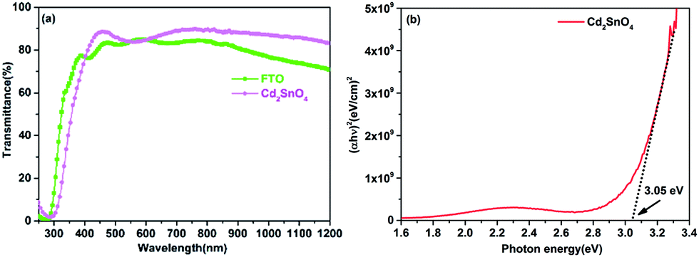 | ||
| Fig. 1 (a) Transmittance spectra of different transparent conductive oxide substrates with similar sheet resistivity of 10 Ω per square and (b) plot of (αhν)2 versus photon energy (hν) for Cd2SnO4 film. | ||
The UPS spectrum was obtained to calculate the work function of the Cd2SnO4 layer, as shown in Fig. 2. According to the linear fit at the secondary electron onset, we can obtain the sample inelastic cut-off (ECutoff) of 17.02 eV. In the valence band emission region, the distance between the valence band (EVBM) and Fermi edge (EFermi) can be estimated to 3.03 eV from the intercept of the linear fitting plot. Based on the Einstein's photoemission law, the work function (Φ) can be described as follows:32
| Φ = hν − (ECutoff − EFermi) | (2) |
| χ = Φ + EVBM − Eg | (3) |
 | ||
| Fig. 2 UPS spectrum of Cd2SnO4 film on glass. | ||
According to eqn (3), we can obtain an χ value of 4.18 eV for the Cd2SnO4 film. This electron affinity for Cd2SnO4 film is comparable to that of FTO (4.4 eV (ref. 28)) transparent conductive oxide film. This indicates that the Cd2SnO4 film shows a compatible energy level for a transparent conductive oxide substrate.
To investigate the effect of energy band matching at the Cd2SnO4/TiO2 interface, the thermal equilibrium energy band diagram of the Cd2SnO4/TiO2 interface is shown in Fig. 3. Typically, the energy band parameters of TiO2 are reported in another study.33 The energy band parameters of the TiO2 and Cd2SnO4 layers are listed in ESI Table S1.† In the front contact region of the photovoltaic devices, the electron-transporting layer/transparent conductive oxide layer interface has a key influence on electron collection. The high resistivity of the TiO2 layer coated on the Cd2SnO4 layer provides reasonable electronic levels with favorable electron collection, associating with low recombination at the TiO2/electrode interface.34 As shown in Fig. 3, the work function of the TiO2 layer is higher than that of Cd2SnO4 at the Cd2SnO4/TiO2 interface, which renders it possible for charge injection and collection from TiO2 to the electrode. The energy band bending of 0.45 eV occurs in this heterojunction. The very small band barrier ΔEc of 0.08 eV exists at the interface, enhancing the interfacial charge transport and decreasing the electronic reflux and charge accumulation.35 It is reasonable to form an energy band structure-matching between the Cd2SnO4 electrode and electron-transporting layer for an efficient charge transport process. This suggests that the Cd2SnO4 layer is a promising and excellent transparent conductive oxide substrate for TiO2-based perovskite solar cells.
 | ||
| Fig. 3 Energy band structure diagram of the TiO2/Cd2SnO4 layer interface. | ||
To investigate the effect of interfacial recombination on the Cd2SnO4 and TiO2 layers, Cd2SnO4 (and FTO)/bl-TiO2/spiro-OMeTAD/Au devices were prepared. Fig. 4(a–e) shows SEM and AFM images of the bl-TiO2 on FTO and Cd2SnO4 substrates and the dark current density–voltage characteristics of the TCO/TiO2/spiro-OMeTAD/Au devices. Their interface quality plays a key role in the performance of devices. As can be seen in Fig. 4(a–d), the morphology of TiO2 is strongly dependent on the substrate. TiO2 on the FTO substrate shows a large size compared to that on the Cd2SnO4 substrate. Highly dense and homogeneous TiO2 films were formed by spray pyrolysis. AFM was carried out to study the morphology of different substrates. The AFM images of FTO and Cd2SnO4 substrates are shown in ESI Fig. S1.† According to the AFM images, the surface root-mean-square (RMS) roughness of FTO, Cd2SnO4, FTO/TiO2, and Cd2SnO4/TiO2 were 12.2 nm, 7.24 nm, 8.16 nm, and 3.97 nm, respectively. The Cd2SnO4 and Cd2SnO4/TiO2 layers show lower surface roughness as compared to the FTO substrate. Note that a smooth and compact TiO2 coating layer can effectively be formed on the Cd2SnO4 substrate due to the smaller grain size of Cd2SnO4. As can be observed from the dark current density–voltage curves of TCO/TiO2/spiro-OMeTAD/Au devices, the Cd2SnO4-based device shows a dark current density of 10−5 mA cm−2, which is lower than that of the FTO-based device. This indicates that charge recombination can be decreased at the electron-transporting layer/Cd2SnO4 electrode interface. The higher surface roughness increases the interfacial charge recombination and reduces electron collection from the TiO2 layer to the electrode.17
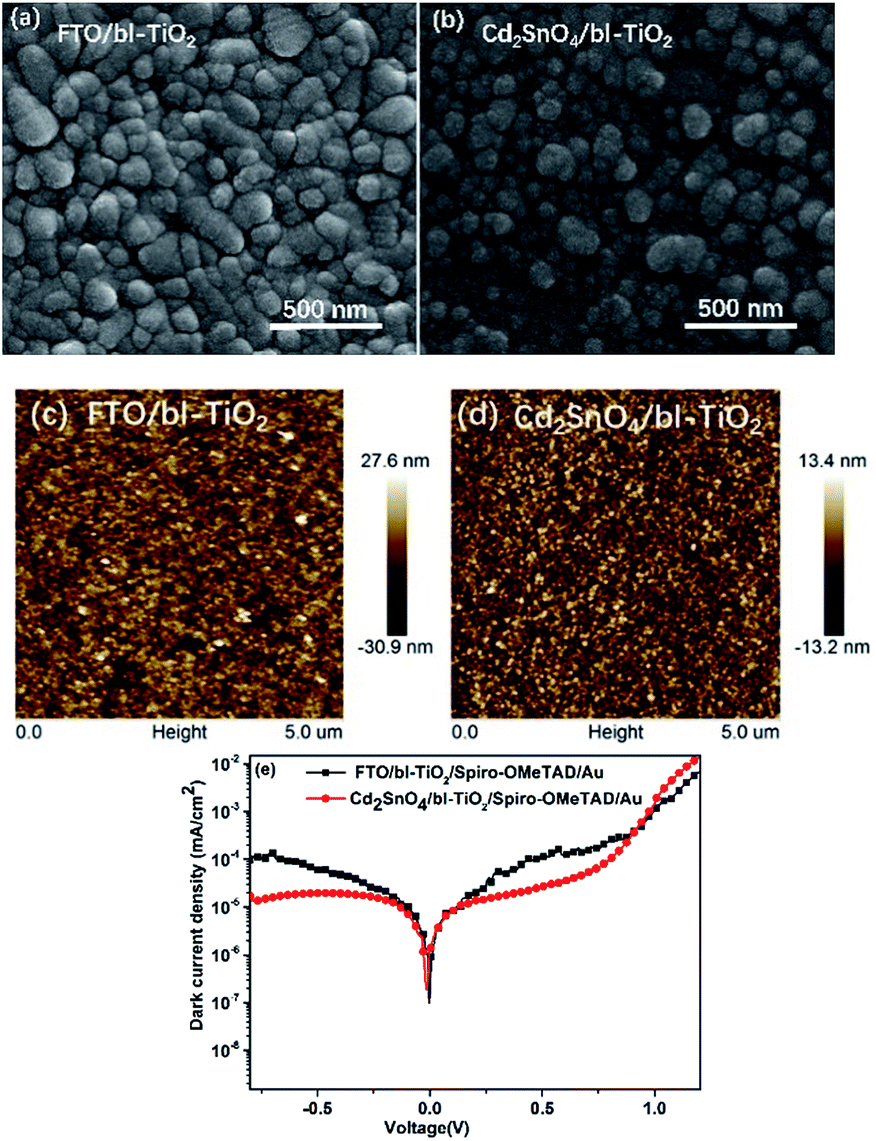 | ||
| Fig. 4 SEM and AFM images of bl-TiO2 on FTO (a and c) and Cd2SnO4 (b and d) substrates; (e) dark current density–voltage characteristics of the FTO and Cd2SnO4/TiO2/spiro-OMeTAD/Au devices. | ||
Fig. 5(a and b) shows the typical structure configuration of perovskite device and the energy level alignment of the perovskite device employing the Cd2SnO4-based substrate. The glass/TCO/TiO2/CH3NH3PbI3−xClx/spiro-MeOTAD/Au devices were fabricated. The detailed preparation approaches are discussed in the methods section. The perovskite films absorb the incident photons under light irradiation, resulting in rapid generation, drift, and diffusion of excitons in the built-in electric field. Then, photoexcited charge transfer occurs at the TiO2/perovskite/HTM interface.36 The holes of the valence band maximum position are extracted from the HOMO level of HTM. The electrons are injected into the conduction band minimum position of the TiO2 layer. Thus, the electrons are collected by the Cd2SnO4 electrode. The matching energy-band alignment can ensure smooth carrier transport between the TiO2 and Cd2SnO4 electrode layers.
 | ||
| Fig. 5 (a) Structure of perovskite devices and (b) energy band diagram of the perovskite devices. Cross-sectional SEM image of the devices: (c) glass/FTO/TiO2/CH3NH3PbI3−xClx/spiro-MeOTAD/Au and (d) glass/Cd2SnO4/TiO2/CH3NH3PbI3−xClx/spiro-MeOTAD/Au. | ||
Fig. 5(c and d) shows cross-sectional SEM images of the FTO and Cd2SnO4-based devices. As can be seen in the two devices, the interfacial layers are effectively contacted to ensure charge transfer. These homogeneous and dense perovskite films fabricated using a high precursor concentration method were formed on the mp-TiO2 layer. The morphology of the perovskite film has been reported in a previous study.37 Compared to the cross-sectional SEM images of the two devices, the thickness of FTO substrate can be up to ∼400 nm. As abovementioned, both substrates have a similar sheet resistivity of 10 Ω per square. The thickness of Cd2SnO4 substrate is only about 250 nm. This is important for regulating the film thickness of the front electrode, which presumably has an influence on the optical properties of the perovskite solar cells. A thicker transparent conductive oxide film decreases the optical transmittance and further affects the photovoltaic performance.
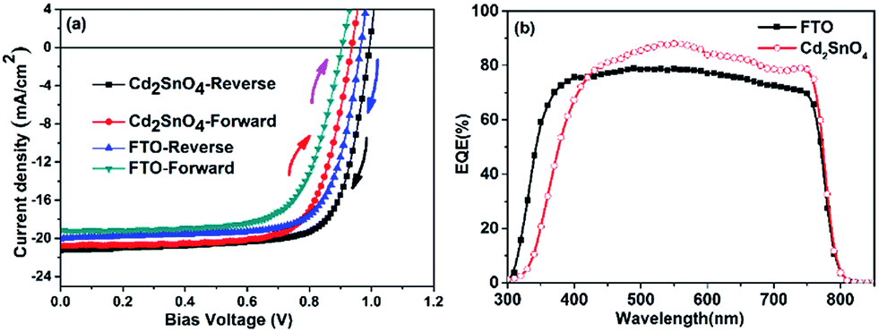
Fig. 6(a) shows the J–V curves of the FTO and Cd2SnO4-based devices obtained under an air mass 1.5 global irradiation of 100 mW cm−2 for reverse and forward scanning. Table 2 lists the average photovoltaic parameters for the FTO and Cd2SnO4-based perovskite devices. Histograms of their device efficiency are shown in ESI Fig. S2.† Typically, the devices were investigated with a delay time of 10 ms from −0.1 V to 1.1 V for the reverse and forward scanning direction. Both the FTO and Cd2SnO4-based devices exhibit slight hysteresis, as shown in Fig. 6(a), which is similar to the behavior of perovskite solar cells with a TiO2 architecture reported in other studies possibly due to the unusual defect physics and grain boundary ion migration.38–40 The average photovoltaic performance parameters for the FTO-based device exhibit a PCE of 14.05%, open circuit voltage (Voc) of 0.97 V, short-circuit current density (Jsc) of 20.04 mA cm−2, and fill factor (FF) of 72.65% for the reverse scanning direction, and a Jsc of 19.14 mA cm−2, Voc of 0.90 V, FF of 70.2%, and PCE of 12.1% for the forward scanning direction. For the Cd2SnO4-based device, the performance shows a PCE of 15.58%, Voc of 0.99 V, Jsc of 21.24 mA cm−2, and FF of 73.83% for the reverse scanning direction, and a PCE of 14.06%, Voc of 0.94 V, Jsc of 20.79 mA cm−2, and FF of 72.2% for the forward scanning direction. As shown in Table 2, the Jsc, Voc, and FF for the Cd2SnO4-based device are higher than those for the FTO-based device. Specifically, a higher photocurrent can be expected from the more incident photons absorbed by the perovskite film. Due to the high transmittance in the visible spectra region of the transparent conductive oxide layer, as shown in Fig. 1, more incident photons reach the perovskite layer from the front contact. More absorption and transition from the valance band to the conduction band occur in the photoactive layer. In addition, due to the high roughness of the FTO/TiO2 interface, trapping states distributed in the energy band gap increase at the heterojunction interface, leading to an energy level offset that is deviated from the predicted level position.41 In this case, electron–hole recombination loss may occur due to the undesirable charge separation efficiency in the device, contributing to the lower Voc and FF.17 Fig. 6(b) shows the external quantum efficiency of the devices. The spectral response of the Cd2SnO4-based devices begins at ∼320 nm, which exhibits narrow response compared to that of the FTO based-devices due to the lower optical energy band gap. This is consistent with the transmittance spectra, as shown in Fig. 1(a). The EQE dramatically increases in the 500–600 nm spectral range. This suggests that efficient charge extraction and transportation occur in the built-in electric field for the Cd2SnO4-based device, leading to a higher photogenerated current.
 | ||
| Fig. 6 (a) Typical J–V curve of the FTO and Cd2SnO4-based devices obtained under AM1.5 light irradiation for the reverse and forward scanning directions and (b) EQE spectra of the devices. | ||
| Substrate | Jsc (mA cm−2) | Voc (V) | FF (%) | PCE (%) |
|---|---|---|---|---|
| FTO | 20.04 ± 1.39 | 0.97 ± 0.03 | 72.65 ± 2.12 | 14.05 ± 1.3 |
| Cd2SnO4 | 21.24 ± 1.96 | 0.99 ± 0.04 | 73.83 ± 1.14 | 15.58 ± 3.25 |
We further analyzed the I–V properties of the solar cells. According to the Shockley equation and equivalent circuit model for a single heterojunction solar cell, the I–V characteristic equation is described as follows:42,43
 | (4) |
 | (5) |
 | (6) |
For perovskite devices, the shunt resistances of the devices are estimated to be 3000 Ω cm2.42 The value of Rs is the intercept by linear curve fitting, as shown in Fig. 7(a). The series resistance of FTO and Cd2SnO4-based devices was estimated to be 1.63 Ω cm2 and 1.46 Ω cm2, respectively. This indicates that the Cd2SnO4-based device shows a lower series resistance due to the thickness of the films. Similarly, the value of J0 can be obtained by linear curve fitting, as shown in Fig. 7(b). The values of the intercept for the FTO and Cd2SnO4-based devices are −12.85 and −13.67 and the recombination current density can be estimated to be 2.62 × 10⁻⁶ mA cm−2 and 1.16 × 10⁻⁶ mA cm−2, respectively. The lower J0 of the Cd2SnO4-based devices indicates that interface charge recombination loss can be effectively decreased by interfacial engineering, leading to a higher Voc and FF.
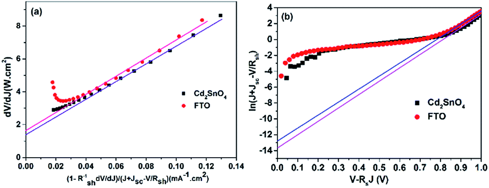 | ||
Fig. 7 (a) Plots of  against against  and (b) plots of ln(J + Jsc − V/Rsh) against (V − RsJ). and (b) plots of ln(J + Jsc − V/Rsh) against (V − RsJ). | ||
The steady-state photoluminescence and time-resolved photoluminescence spectra were acquired to explore the photoinduced charge dynamical process in the devices. We prepared CH3NH3PbI3−xClx films on FTO/TiO2 and Cd2SnO4/TiO2 substrates. Fig. 8(a) presents the steady-state photoluminescence spectra for CH3NH3PbI3−xClx films on FTO/TiO2 and Cd2SnO4/TiO2 substrates. The PL intensity at 773 nm for the perovskite film on Cd2SnO4/TiO2 clearly shows a decrease as compared to that for the perovskite film on the FTO/TiO2 substrate. This indicates that the charge dissociation process on the Cd2SnO4 electrode with TiO2 layer is more efficient. Fig. 8(b) shows the time-resolved photoluminescence spectra of the perovskite films on various substrates. The PL decay lifetimes were obtained by fitting the data to the biexponential decay function containing a fast decay component (τ1) and a slow decay component (τ2). The detailed fitting parameters are summarized in ESI Table S2.† The fast decay component might be considered as the result of the quenching of free electrons in the perovskite via transport to TiO2. The slow decay component can be originated from the radiative recombination of the free carriers in the perovskite film.15,44,45 For the FTO/TiO2/CH3NH3PbI3−xClx film sample, the fast decay lifetime was 0.55 ns and the slow decay lifetime was 14.4 ns, whereas the weight fractions were 67.7% and 32.3%, respectively. This indicates that the decay of free charges was dominated by charge collection through the TiO2/perovskite interface. However, the τ1 and τ2 for the Cd2SnO4/TiO2/CH3NH3PbI3−xClx sample decreased to 0.46 ns and 9.26 ns, respectively. The weight fraction of the fast decay component drastically increased to 89.6%. The Cd2SnO4 electrode facilitates faster charge transfer from perovskite to TiO2. The electrode can enable the much faster and more efficient collection of the photogenerated electrons due to lower interfacial recombination loss as discussed above, leading to the enhancement of photovoltaic performance.15
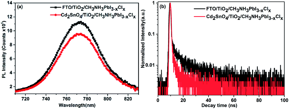 | ||
| Fig. 8 (a) Steady-state photoluminescence spectra and (b) time-resolved photoluminescence spectra of the CH3NH3PbI3−xClx films on the FTO/TiO2 and Cd2SnO4/TiO2 substrates. | ||
Furthermore, we investigated the long-term device stability of the Cd2SnO4-based device in a relative humidity of ∼10% at room temperature, as shown in Fig. 9. The stability of the FTO-based device is shown in ESI Fig. S3.†
 | ||
| Fig. 9 Stability of the device stored in a relative humidity of ∼10% for 60 days. | ||
When the device was stored for 60 days, the Voc showed a slight decay. The device efficiency drops ∼35% after 60 days. The FF and Jsc of the device maintained 85% of its initial value. For the FTO-based device, the FF and Jsc of the device can retain ∼95% of the initial value when the device was stored for 25 days. The dense HTM layer hinders the penetration of water molecule for a long time, which can improve the device stability. The device parameters did not show significant degradation in two months. However, the instability of perovskite devices is the main issue while exposing them to an ambient air environment. Moisture degradation and photooxidation may take place at the interface in the presence of oxygen, light, and moisture. Further enhancements of the stability of the device are required. Interface modification on TiO2/CH3NH3PbI3−xClx may be an effective method to improve the stability. In further studies, we believe that the introduction of surface treatment technology by passivation surface defects of TiO2 layer to protect the perovskite devices from corrosion by moisture and oxygen is required. Solving the extrinsic and intrinsic degradation problem of the perovskite devices, which have potential for large scale applications, overcomes the major obstacles in their practical applications.
Conclusion
We demonstrated a new structure of perovskite solar cell using a Cd2SnO4 transparent conducting oxide substrate. Owing to its higher electrical conductivity, optical transmission in the visible range, and lower surface roughness as compared to those of FTO, a higher PCE of 15.58% for the Cd2SnO4-based perovskite solar cell was obtained. The energy band structure and interfacial characteristics of Cd2SnO4/TiO2 interface were investigated. The results showed that the matching energy band alignment could ensure smooth carrier transport and collection between the TiO2 and Cd2SnO4 electrode layers, which suggests that Cd2SnO4 transparent conducting oxide would be the most promising candidate for high performance perovskite solar cells.Acknowledgements
This work was financially supported by the Science and Technology Program of Sichuan Province (No. 2016GZX0272) and the Innovation Program of Sichuan University (No. 201510611374, No. 201510610799 and No. 201510610437).References
- D. P. McMeekin, G. Sadoughi, W. Rehman, G. E. Eperon, M. Saliba, M. T. Horantner, A. Haghighirad, N. Sakai, L. Korte, B. Rech, M. B. Johnston, L. M. Herz and H. J. Snaith, Science, 2016, 351, 151–155 CrossRef CAS PubMed.
- D. Bi, W. Tress, M. I. Dar, P. Gao, J. Luo, C. Renevier, K. Schenk, A. Abate, F. Giordano, J. P. Correa Baena, J. D. Decoppet, S. M. Zakeeruddin, M. K. Nazeeruddin, M. Gratzel and A. Hagfeldt, Sci. Adv., 2016, 2, e1501170 Search PubMed.
- D. Liu, L. Wu, C. Li, S. Ren, J. Zhang, W. Li and L. Feng, ACS Appl. Mater. Interfaces, 2015, 7, 16330–16337 CAS.
- Q. Tai, P. You, H. Sang, Z. Liu, C. Hu, H. L. W. Chan and F. Yan, Nat. Commun., 2016, 7, 11105 CrossRef CAS PubMed.
- X. Li, D. Bi, C. Yi, J.-D. Décoppet, J. Luo, S. M. Zakeeruddin, A. Hagfeldt and M. Grätzel, Science, 2016, 353, 58–62 CrossRef CAS PubMed.
- Z. Zhou, J. Xu, L. Xiao, J. Chen, Z. A. Tan, J. Yao and S. Dai, RSC Adv., 2016, 6, 78585–78594 RSC.
- L. F. Zhu, Y. Z. Xu, J. J. Shi, H. Y. Zhang, X. Xu, Y. H. Zhao, Y. H. Luo, Q. B. Meng and D. M. Li, RSC Adv., 2016, 6, 82282–82288 RSC.
- Z. Zhang, X. Yue, D. Wei, M. Li, P. Fu, B. Xie, D. Song and Y. Li, RSC Adv., 2015, 5, 104606–104611 RSC.
- D. Liu, C. Liu, L. Wu, W. Li, F. Chen, B. Xiao, J. Zhang and L. Feng, RSC Adv., 2016, 6, 51279–51285 RSC.
- X. Xia, W. Wu, H. Li, B. Zheng, Y. Xue, J. Xu, D. Zhang, C. Gao and X. Liu, RSC Adv., 2016, 6, 14792–14798 RSC.
- H. Sohrabpoor, G. Puccetti and N. E. Gorji, RSC Adv., 2016, 6, 49328–49334 RSC.
- W.-C. Lai, K.-W. Lin, Y.-T. Wang, T.-Y. Chiang, P. Chen and T.-F. Guo, Adv. Mater., 2016, 28, 3290–3297 CrossRef CAS PubMed.
- H. Hwang, A. Kim, Z. Zhong, H.-C. Kwon, S. Jeong and J. Moon, Adv. Funct. Mater., 2016, 26, 6545–6554 CrossRef CAS.
- M. Dianetti, F. Di Giacomo, G. Polino, C. Ciceroni, A. Liscio, A. D'Epifanio, S. Licoccia, T. M. Brown, A. Di Carlo and F. Brunetti, Sol. Energy Mater. Sol. Cells, 2015, 140, 150–157 CrossRef CAS.
- Y. Li, L. Meng, Y. M. Yang, G. Xu, Z. Hong, Q. Chen, J. You, G. Li, Y. Yang and Y. Li, Nat. Commun., 2016, 7, 10214 CrossRef CAS PubMed.
- K. Sun, P. C. Li, Y. J. Xia, J. J. Chang and J. Y. Ouyang, ACS Appl. Mater. Interfaces, 2015, 7, 15314–15320 CAS.
- H. Sung, N. Ahn, M. S. Jang, J.-K. Lee, H. Yoon, N.-G. Park and M. Choi, Adv. Energy Mater., 2016, 6, 1501873 CrossRef.
- J. A. Stoke, J. D. Beach, W. C. Bradford and T. R. Ohno, Thin Solid Films, 2014, 562, 254–259 CrossRef CAS.
- X. Wu, Sol. Energy, 2004, 77, 803–814 CrossRef CAS.
- B. A. Korevaar, J. R. Cournoyer, O. Sulima, A. Yakimov and J. N. Johnson, Prog. Photovoltaics Res. Appl., 2014, 22, 1040–1049 CrossRef CAS.
- S. M. Al-Sofiany and H. E. Hassan, J. Alloys Compd., 2015, 651, 149–156 CrossRef CAS.
- R. Kumaravel and K. Ramamurthi, J. Alloys Compd., 2011, 509, 4390–4393 CrossRef CAS.
- R. Mamazza, D. L. Morel and C. S. Ferekides, Thin Solid Films, 2005, 484, 26–33 CrossRef CAS.
- G. Valincius, V. Reipa, V. Vilker, J. T. Woodward and M. Vaudin, J. Electrochem. Soc., 2001, 148, E341–E347 CrossRef CAS.
- R. B. H. Tahar, T. Ban, Y. Ohya and Y. Takahashi, J. Am. Ceram. Soc., 2001, 84, 85–91 CrossRef CAS.
- J. H. Im, I. H. Jang, N. Pellet, M. Gratzel and N. G. Park, Nat. Nanotechnol., 2014, 9, 927–932 CrossRef CAS PubMed.
- J. Tauc, Mater. Res. Bull., 1968, 3, 37–46 CrossRef CAS.
- M. A. Green, A. Ho-Baillie and H. J. Snaith, Nat. Photonics, 2014, 8, 506–514 CrossRef CAS.
- J. Werner, C.-H. Weng, A. Walter, L. Fesquet, J. P. Seif, S. De Wolf, B. Niesen and C. Ballif, J. Phys. Chem. Lett., 2016, 7, 161–166 CrossRef CAS PubMed.
- T. Duong, N. Lal, D. Grant, D. Jacobs, P. Zheng, S. Rahman, H. Shen, M. Stocks, A. Blakers, K. Weber, T. P. White and K. R. Catchpole, IEEE J. Photovolt., 2016, 6, 679–687 CrossRef.
- J. Werner, G. Dubuis, A. Walter, P. Löper, S.-J. Moon, S. Nicolay, M. Morales-Masis, S. De Wolf, B. Niesen and C. Ballif, Sol. Energy Mater. Sol. Cells, 2015, 141, 407–413 CrossRef CAS.
- Y. Park, V. Choong, Y. Gao, B. R. Hsieh and C. W. Tang, Appl. Phys. Lett., 1996, 68, 2699–2701 CrossRef CAS.
- A. Dymshits, A. Henning, G. Segev, Y. Rosenwaks and L. Etgar, Sci. Rep., 2015, 5, 8704 CrossRef CAS PubMed.
- J. Shi, X. Xu, D. Li and Q. Meng, Small, 2015, 11, 2472–2486 CrossRef CAS PubMed.
- Z. Zhou, S. Pang, Z. Liu, H. Xu and G. Cui, J. Mater. Chem. A, 2015, 3, 19205–19217 CAS.
- G. Xing, B. Wu, S. Chen, J. Chua, N. Yantara, S. Mhaisalkar, N. Mathews and T. C. Sum, Small, 2015, 11, 3606–3613 CrossRef CAS PubMed.
- D. Liu, C. Liu, L. Wu, W. Li, F. Chen, B. Xiao, J. Zhang and L. Feng, RSC Adv., 2016, 6, 51279–51285 RSC.
- S. Wozny, M. Yang, A. M. Nardes, C. C. Mercado, S. Ferrere, M. O. Reese, W. Zhou and K. Zhu, Chem. Mater., 2015, 27, 4814–4820 CrossRef CAS.
- H.-S. Kim and N.-G. Park, J. Phys. Chem. C, 2014, 5, 2927–2934 CAS.
- Y. Shao, Y. Fang, T. Li, Q. Wang, Q. Dong, Y. Deng, Y. Yuan, H. Wei, M. Wang, A. Gruverman, J. Shield and J. Huang, Energy Environ. Sci., 2016, 9, 1752–1759 CAS.
- Q.-K. Wang, R.-B. Wang, P.-F. Shen, C. Li, Y.-Q. Li, L.-J. Liu, S. Duhm and J.-X. Tang, Adv. Mater. Interfaces, 2015, 2, 1400528 CrossRef.
- J. Shi, J. Dong, S. Lv, Y. Xu, L. Zhu, J. Xiao, X. Xu, H. Wu, D. Li, Y. Luo and Q. Meng, Appl. Phys. Lett., 2014, 104, 063901 CrossRef.
- J. Qing, H.-T. Chandran, Y.-H. Cheng, X.-K. Liu, H.-W. Li, S.-W. Tsang, M.-F. Lo and C.-S. Lee, ACS Appl. Mater. Interfaces, 2015, 7, 23110–23116 CAS.
- P.-W. Liang, C.-Y. Liao, C.-C. Chueh, F. Zuo, S. T. Williams, X.-K. Xin, J. Lin and A. K. Y. Jen, Adv. Mater., 2014, 26, 3748–3754 CrossRef CAS PubMed.
- Y. Shi, Y. Xing, Y. Li, Q. Dong, K. Wang, Y. Du, X. Bai, S. Wang, Z. Chen and T. Ma, J. Phys. Chem. C, 2015, 119, 15868–15873 CAS.
Footnotes |
| † Electronic supplementary information (ESI) available: Detailed energy band parameters of the TiO2 and Cd2SnO4 films; AFM images for FTO and Cd2SnO4 layers; histograms of their devices efficiency; stability of FTO-based device stored in relative humidity of ∼10% for 27 days. See DOI: 10.1039/c6ra27146d |
| ‡ These authors contributed equally to this work. |
| This journal is © The Royal Society of Chemistry 2017 |