
 Open Access Article
 This Open Access Article is licensed under a Creative Commons Attribution-Non Commercial 3.0 Unported Licence
Controllable gold-capped nanoporous anodic alumina chip for label-free, specific detection of bacterial cells†
Do-Kyun Kim‡
a,
Dong Min Kim‡b,
Seung Min Yoo *a and
Sang Yup Lee*a
*a and
Sang Yup Lee*a
aDepartment of Chemical and Biomolecular Engineering (BK21 Plus Program), BioProcess Engineering Research Center, KAIST, Daejeon, 34141, Republic of Korea. E-mail: smyoo@kaist.ac.kr; leesy@kaist.ac.kr; Fax: +82 42 350 8800; Tel: +82 42 350 8814
bCenter for Applied Life Science, Hanbat National University, Daejeon, 34158, Republic of Korea
First published on 28th March 2017
Abstract
We describe the development of a gold-capped nanostructured porous anodic alumina (PAA) chip, which makes use of localized surface plasmon resonance and interferometry for the label-free and specific detection of pathogenic bacterial cells via changes in relative reflected intensity (RRI) and wavelength shift. This chip is composed of PAA and gold layers that provide a reproducible and sensitive RRI and wavelength shift. We investigated the effects of varying the thicknesses of the PAA and gold layers on the optical responses of the chip. With this chip, we successfully detected and identified Pseudomonas aeruginosa in a proof-of-concept experiment; this chip can detect bacterial cells in a quantitative manner with a detection limit of 20 CFU per assay. Further, this chip based system can clearly identify target bacterial species in a multiplexed mode with high specificities on a single chip, so will be useful for the detection of various pathogenic microbes.
Introduction
Optical biosensors can provide rapid, easy-to-use, and cost-effective sensing or detection of various biomolecules. In particular, plasmonic biosensors exhibit superior sensitivity and multiplexing capability, so have been developed for the detection of biomolecules; several companies are ready to supply such sensors and some are already commercially available.1 The sensing capabilities of plasmonic biosensors arise through control of the composition and features of their plasmonic nanostructures.Several plasmonic nanostructures have been developed, including coupled nanoparticle arrays, periodic or random nanohole arrays, gold-capped mushroom arrays, and arrays of nanoimprinted nanodisks or nanosquares.2–10 Of these nanostructures, gold-coated nanostructured porous anodic alumina (PAA) has been found to exhibit enhanced optical properties through the combination of two sensing approaches, namely localized surface plasmon resonance (LSPR) spectroscopy and interferometry.11–16 Nanostructured PAA is composed of an alumina lattice template with periodic nanopores of uniform size and a regular diameter along their length.17,18 PAA has several advantages such as high stability at physiological pH levels, mechanical robustness, biocompatibility, and the facile fabrication of self-hexagonal pore arrangements, making it suitable for use in the preparation of large-scale templates that are cost-effective and provide stable optical biosensing without the need for further passivation. In the gold-capped nanostructured PAA chip, the wavelength shift and the change in relative reflected intensity (RRI) are enhanced through the combination of interferometry and LSPR.13,15,16,19 Interference causes a wavelength shift and the change in RRI. The surface binding event leads to a change in the wavelength-dependent refractive index of sensing membrane. A very small change in the interfacial refractive index of the surrounding media can be detected using LSPR, which is greatly affected by the binding of biomolecules. Thus, this chip results in a significant change in sensitivity, as observed by both interferometry and LSPR.13,15,16,19 Moreover, the gold layer is biocompatible and enables the easy functionalization of biomolecules and thus the optimal attachment of biomolecules via a self-assembled monolayer (SAM). These advantages mean that such gold-capped PAA nanostructures have been successfully utilized in various biosensors, including devices for the detection of DNA,16 proteins,12–14 chemicals,14,20 and cancer cells.21
Here, we describe a gold-capped nanostructured PAA chip for the label-free and specific detection of bacterial cells. There has been no previous report, to our knowledge, of a gold-capped nanostructured PAA bacterial cell sensing chip. We demonstrate that RRI and wavelength shift can be tuned by controlling the thicknesses of the PAA and gold layers. For our proof-of-concept experiment, we adopted Pseudomonas aeruginosa and its aptamer as a model system. Specific bacterial cells can be successfully detected without cross-reactivity by employing an aptamer-functionalized chip in multiplex mode. Therefore, we anticipate that the chip developed here will prove useful in the high specificity detection of bacterial cells.
Experimental
Materials
All chemicals were purchased from Sigma-Aldrich Co. Oligonucleotides were synthesized at Genotech Co (Korea). The sequences of the P. aeruginosa-specific aptamers (Pae-apt) are 5′-CCCCCGTTGCTTTCGCTTTTCCTTTCGCTTTTGTTCGTTTCGTCCCTGCTTCCTTTCTTG–(CH2)3–SH-3′.22 Reference bacteria except Escherichia coli were obtained from the American Type Culture Collection (ATCC; USA) and the Korean Collection for Type Cultures (KCTC; Korea), and cultured according to the provided instructions. The bacteria used in this study are as follows: P. aeruginosa PA01 (ATCC 27853), Salmonella typhimurium (KCTC 2053), Lactobacillus acidophilus (KCTC 3164), and E. coli DH5a.Preparation of gold-capped PAA nanostructure chip
The PAA layer nanostructure was fabricated with two-step anodizing method (Fig. 1a). Prior to anodizing procedure, glass slide (76 × 26 × 1 mm3) was treated by ultrasonication for 10 min in acetone, ethanol, and ultrapure deionized water and then deposited with aluminum (3 μm in height) by using a thermal evaporator (SVC-700TM/700-2, Sanyu Electron Co. Ltd). The growth rate in thickness was monitored by Inficon SQM-160 monitor and manually adjusted to 1.0 Å s−1 (Fig. 1a-i). After that, the substrate was sealing with liquid silicon for 24 h. The first anodizing step was carried out under the voltage of 40 V in a 0.3 M oxalic acid solution for 40 s to 14 min (PAA layer thickness = 0.05–1 μm) (Fig. 1a-ii) while keeping the anode temperature at 10 °C by vigorously stirring. After that, the Al-deposited slide glass was immersed into the solution containing a mixture of phosphoric acid (1.8%, w/v) and chromic acid (2%, w/v), resulting in a partial removal of the generated PAA layer on the Al-deposited slide glass (Fig. 1a-iii). Then the second anodizing step was carried out with the same conditions as described in the first anodizing step for 40 s to 14 min (Fig. 1a-iv). The PAA layers with various thicknesses were obtained by changing the time for the anodizing steps. For creating multiple spots on a chip, a multispot (3 mm in diameter) stainless steel mask was placed on the surface of PAA nanostructured chip (Fig. 1a-v). After that, the PAA chip was plated with a 50 Å Cr layer and a 0–300 Å Au layer (Fig. 1a-vi). The Cr was used as adhesion layer between aluminum oxide (grown on Al substrate) and Au.23 The different thickness of Au layer was deposited onto the PAA layer using a thermal evaporator (SVC-700TM/700-2, Sanyu Electron Co. Ltd) for different time. The growth rate of thickness was monitored by Inficon SQM-160 monitor and was manually adjusted to 1.0 Å s−1. The uniform nanostructure of the spots on the chip was confirmed by AFM image (ESI, Fig. S1†).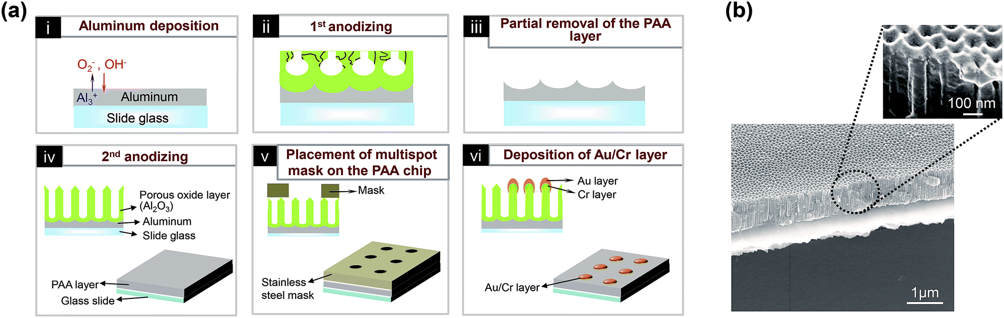 | ||
| Fig. 1 Gold-capped nanoporous anodic alumina chip. (a) Schematic illustration of the process for the fabrication of a gold-capped nanostructured PAA chip. (b) Cross-sectional SEM image of the resulting chip. | ||
Detection of bacterial cells
Ten μM thiol-modified aptamer in 1 M KH2PO4 (pH 6.7) was incubated on the chip at room temperature (RT) for 4 h and excessive DNAs were washed tree times with 0.2% (w/v) sodium dodecyl sulfate (SDS) for 5 min. The bacterial cells samples were prepared at the concentrations of 101 to 109 CFU mL−1 with phosphate buffered saline (PBS) solution and these samples were incubated onto the different spots of the chip at RT for 1 h under the humidified condition. After washing three times with PBS for 5 min, the chips were dried under a nitrogen stream. The wavelength spectra from the chip were measured before and after incubating of target cells under ambient conditions.Instrumentation
The optical measurement system for the evaluation of the optical responses on the chip was based on a spectroscopy system. The optical system was equipped with a light source (wavelength range, 360–2000 nm), spectrophotometer (wavelength range, 200–1100 nm) and an optical fiber probe bundle (fiber core diameter, 300 μm; wavelength range, 250–900 nm) as a spectroscopy system, purchased from Ocean Optics (USA). All wavelength spectra were taken from 350 to 850 nm in air at RT. Scanning electron microscopic (SEM) images of the chip were obtained using Hitachi SEM equipment (S-4800; Hitachi, Japan). The optical probe was fixed on the stand in the vertical direction to the stage and a chip was placed on the X–Y–Z axis stage. White light, emerging from an optical fiber bundle provided incident light, and this light was reflected upon hitting the chip surface coupled into the detection probe of the optical fiber bundle and analyzed by a spectrometer (ESI, Fig. S2†).Results and discussion
Effects of varying the thicknesses of the PAA and gold layers on the optical responses of a gold-capped nanostructured PAA chip
Fig. 1a shows a schematic illustration of the process for the fabrication of the nanostructured PAA chip and SEM images of the resulting chip. The details of the fabrication process can be found in the Experimental section. Briefly, PAA layer is firstly deposited on a slide glass with a two-step anodizing process, which provides a uniform surface and enables interferometry-induced wavelength shifts.15,16 The neighboring pore distance in this highly uniform chip is approximately 120 nm (Fig. 1b); it is well-known that distances between the nanopores in nanoporous structures that are less than 50 nm result in low sensitivity.13,19 A gold layer is then coated onto the PAA layer, which leads to dramatic increases in the wavelength shift and the RRI, as measured with LSPR and interferometry.13,15,16The LSPR and interferometric properties of the chip depend on the thickness of the PAA and gold layer; hence we investigated the effects of varying the PAA and gold layer thickness on the wavelength shift and the RRI.15,16 First, chips were fabricated with various PAA layer thicknesses (50, 100, 250, 500, 750, and 1000 nm) and each individual chip was coated with a 10 nm thick gold layer (see ESI, Fig. S3†). It was found that the RRI decreases with increases in the PAA layer thickness up to 500 nm, but becomes saturated above this thickness. The number of fringes increased with the thickness of the PAA layer. This increase arises because the number of fringe depends on the thickness of product, as given by eqn (1), Fabry–Pérot equation, where, m is the order of the interference maximum, λ is wavelength of light, n is reflective index, L is thickness of product.
| mλ = 2nL | (1) |
These observations are in good agreement with those of previous reports.15,16
We also investigated the effects of varying the thickness of the gold layer on the optical responses. Chips with various PAA layer thicknesses in the range 50 to 1000 nm were coated with gold layers with thicknesses in the range 0 to 30 nm. When the Au layer is thicker than 10 nm, the RRI decreases and the peak shifts to a shorter wavelength (Fig. 2; ESI, Fig. S3 and S4†). This trend was observed for all the chips with different PAA layer thicknesses. This might be due to a coverage of porous nanostructure by Au layer deposition on PAA layer and thus lead to the disappearance of nanoporous structure and the change of interferometric and LSPR properties. The chip with a 5 nm Au layer undergoes a red shift in the wavelength and low RRI, bearing no relation to the above trend (Fig. 2; ESI, Fig. S3 and S4†). This effect probably arises because a coverage thickness of 5 nm is insufficient to enhance the optical response. We used a chip with a 1 μm thick PAA layer and a 10 nm thick Au layer for the subsequent experiments because of its highly reproducible and reliable wavelength peak.
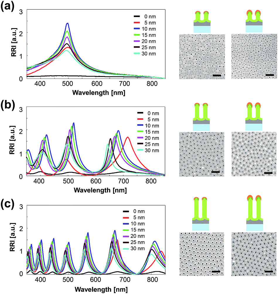 | ||
| Fig. 2 The optical responses of gold-capped nanostructured PAA chips prepared with various PAA and gold layer thicknesses. The panels on the left show the overlaid spectra of the surfaces prepared by varying the gold layer thickness in chips with PAA layer thicknesses of (a) 50 nm, (b) 500 nm, and (c) 1 μm. For each chip with a different PAA layer thickness (a–c), the thickness of the gold layer was varied from 0 to 30 nm. The panels on the right show representative top view SEM images of the surfaces with (left) a 5 nm thick gold layer and (right) a 25 nm thick gold layer on chips with PAA layer thicknesses of (a) 50 nm, (b) 500 nm, and (c) 1 μm. The scale bar is 200 nm. | ||
Effects of aptamer-binding and bacterial cell-binding on the optical responses of the gold-capped nanostructured PAA chip
To investigate the effects of surface binding events on the optical responses of the chip, thiolated aptamers and P. aeruginosa cells were incubated sequentially on the chip. P. aeruginosa is one of the most important pathogenic bacteria that cause nosocomial infections, and thus significantly increase the mortality risk of inpatients.24,25 We used an aptamer modified with thiol group (–SH) to its 3-terminus for thiol–gold interaction.26,27 The chips were functionalized with 10 μM P. aeruginosa-specific aptamer for 4 h and subsequently incubated with 109 CFU mL−1 of P. aeruginosa for 1 h. After washing, the changes in the wavelength shift and the RRI after each process were determined (Fig. 3a). The immobilization of the aptamer on the chip results in a red shift and an increase in the RRI, which is in good agreement with previous results (Fig. 3b).15,16 After bacterial cells have been incubated on the aptamer-functionalized chip, there is a dramatic decrease in the RRI, a slight blue-shift in the wavelength, and the number of fringes remains the same (Fig. 3b; ESI, Fig. S5†). The decrease in the RRI and blue-shift could be due to the large cell size, i.e., the cells cover the nanopores in the chip, lead to the disappearance of nanostructure, and thereby the change of optical properties. No change in the number of fringes probably arises because the incident light can penetrate the cells undergone the dehydration before the sensing procedure and can be reflected within the nanopores of the chip. An aptamer-free chip was also exposed to bacterial cells. No significant change was observed in this chip. These data demonstrate that this chip, when functionalized with species-specific aptamer, successfully detects bacterial cells and that physical adsorption does not occur on the bare chip.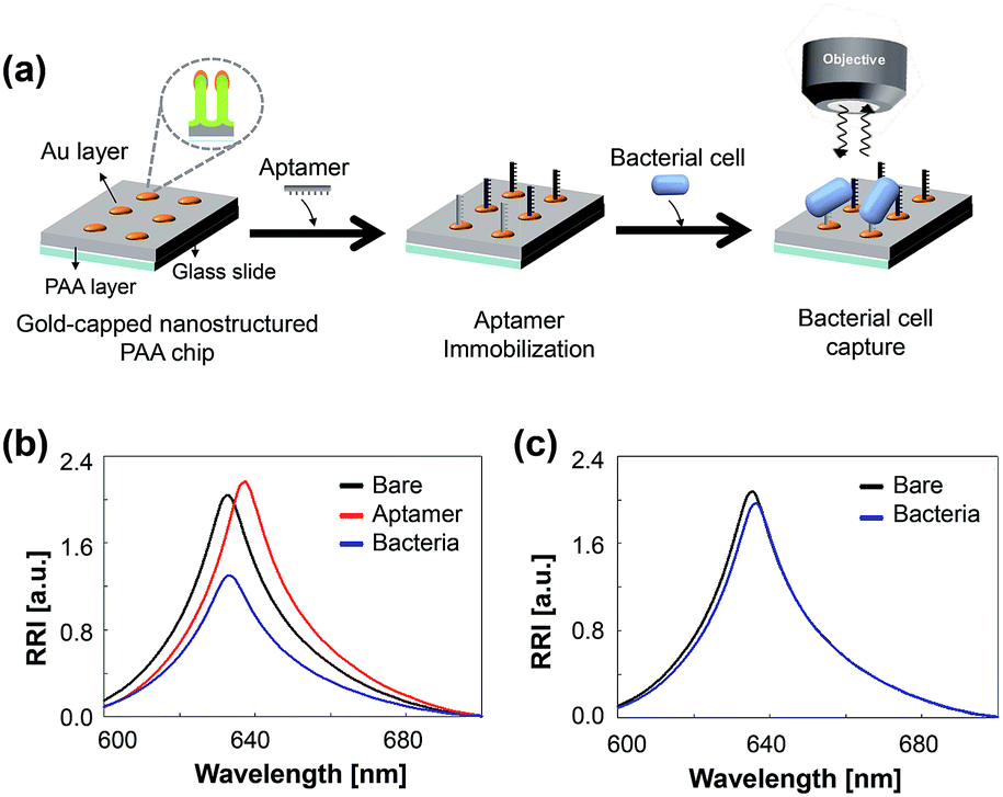 | ||
| Fig. 3 The detection of bacterial cells with the gold-capped nanostructured PAA chip. (a) Schematic illustration of the detection of bacterial cells by an aptamer-functionalized chip. (b) RRI spectra of the bare chip: after immobilizing the aptamer on the chip, and after incubating bacterial cells on the aptamer-functionalized chip. (c) Overlaid RRI spectra of a bare chip and a chip incubated with bacteria without exposure to the aptamer. | ||
We further investigated how the loading volume of the bacterial cells affects the optical responses of this chip. Aptamer-functionalized chips were incubated with various sample volumes (1–4 μL) containing 109 CFU mL−1 of P. aeruginosa. As shown in Fig. 4, the changes in RRI and wavelength shift increases with increases in the sample volume up to 2 μL and becomes saturated at higher volumes. This saturation probably arises because a sample volume of 2 μL is sufficient to cover the surfaces of the spots, which have a diameter of 3 mm, in our chip. Based on these results, the change in the optical responses of the aptamer-bound chip is sufficient to enable the detection with this chip of bacterial cells.
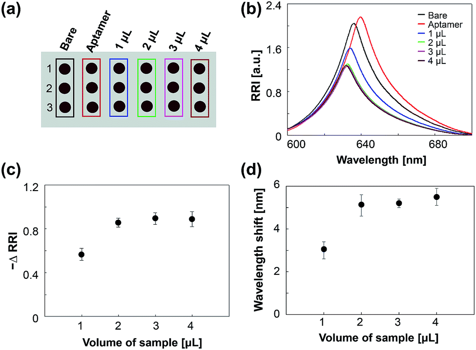 | ||
| Fig. 4 Effects of varying the loading volume of bacterial cells on the optical responses of the gold-capped nanostructured PAA chip. (a) Design of the chip. P. aeruginosa-specific aptamer was immobilized on all spots of the chip except on those shown in the “Bare” column; the chips were subsequently incubated with various sample volumes (1–4 μL) containing 109 CFU mL−1 of bacterial cells or cell-free solution (the “Aptamer” column) in triplicate. (b) Overlaid spectra showing the optical responses of the chips. (c) Plot of the variation in the RRI with the loading volume. (d) Plot of the variation in the wavelength shift with the loading volume. These data were obtained from three measurements; the error bars are the standard deviations. | ||
Sensitivity and specificity of the chip
To determine the detection limits of the chip, thiolated aptamers were immobilized on multiple spots on a chip and samples with various cell concentrations ranging from 101 to 109 CFU mL−1 of P. aeruginosa were vertically spotted in triplicate on the chip (Fig. 5a). The change in RRI and wavelength shift increase linearly with the increase of target bacterial cell concentrations between 103 and 109 CFU mL−1 and become saturated at higher concentrations (Fig. 5b; ESI, Fig. S6†). This result indicates that our chip provides quantitative detection of bacterial cells. The detection limit of this chip was estimated to be 104 CFU mL−1 for the tested bacteria. Thus for this assay volume, our sensing system can detect 20 CFU of bacteria in an assay, which is comparable to other sensing methods including electrical signals,28,29 electrochemical sensing,30–32 SERS,33 LSPR,34 and optical sensing,35,36 which have detection limits in the range 101 to 3 × 10⁴ CFU mL−1.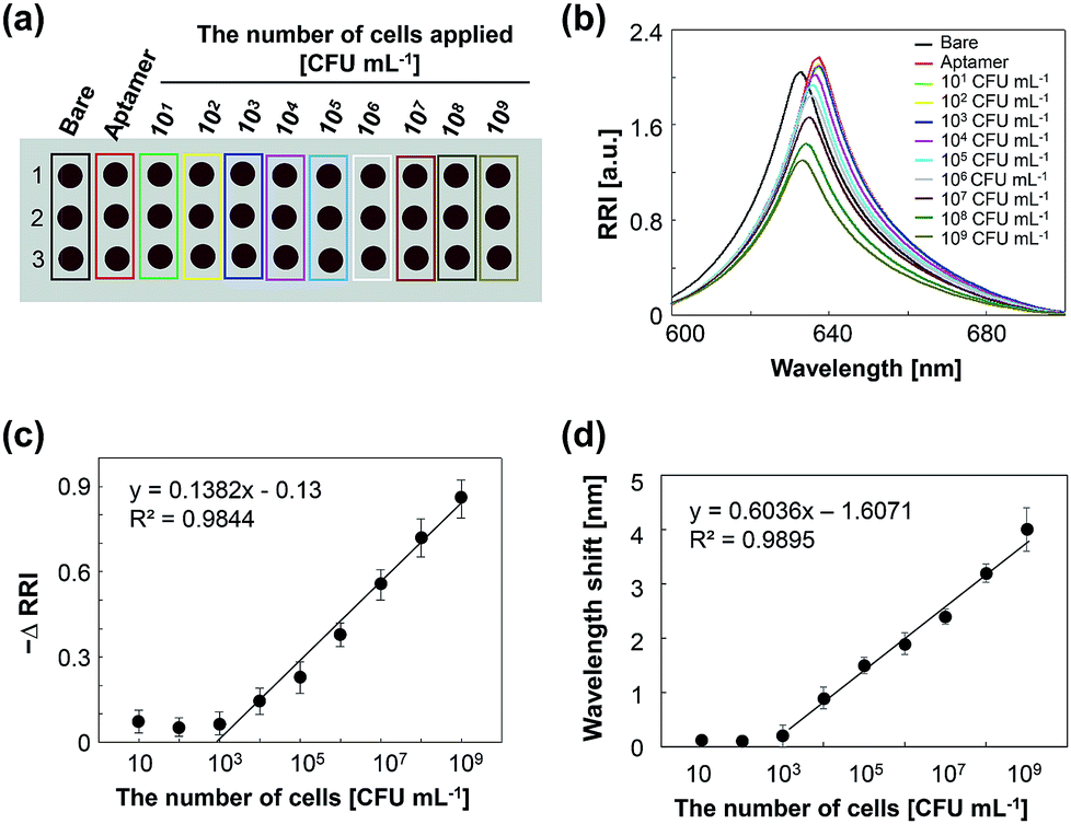 | ||
| Fig. 5 The detection limits of the gold-capped nanostructured PAA chip. (a) Design of the chip. The detection limit was determined by analyzing the optical responses for various cell concentrations ranging from 101 to 109 CFU mL−1 of P. aeruginosa. The chip in the “Bare” column was not treated with any aptamer or cells. The chip in the “Aptamer” column was exposed only to thiolated aptamers, but not to cells. (b) Overlaid spectra showing the optical responses of the chips. (c) Plot of the variation in the RRI with the cell concentration. (d) Plot of the variation in the wavelength shift with the cell concentration. The data were obtained from three measurements; the error bars are standard deviations. | ||
To assess the selectivity of the chip, the P. aeruginosa-specific aptamers were immobilized on all spots of the chip and we observed whether the aptamers specifically bind to the P. aeruginosa (see the inset in Fig. 6). A dramatic reduction in the RRI was observed as a result of the binding between the aptamer and P. aeruginosa (Fig. 6). Incubation with other bacteria or a cell-free PBS solution did not trigger any significant reduction in the RRI. These results demonstrate that our chip can detect target bacterial cells with high specificity.
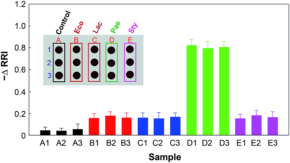 | ||
| Fig. 6 Selectivity of the gold-capped nanostructured PAA chip for the detection of bacterial cells. The inset shows the design of the chip. P. aeruginosa-specific aptamers were immobilized on all spots of the chip and subsequently each bacterial species (109 CFU mL−1) was applied in triplicate to a column (e.g. the deposition of E. coli at B1, B2, and B3). The data were obtained from three measurements; the error bars are standard deviations. Control: cell-free PBS solution; Eco: E. coli; Lac: L. acidophilus; Pae: P. aeruginosa; Sty: S. typhimurium. | ||
Conclusions
We have developed a gold-capped nanostructured PAA chip that uses aptamers for the label-free, specific, and quantitative detection of bacterial cells. This bacterial cell sensing chip has the following advantages. First, the gold-capped nanostructured PAA platform produces highly reproducible and reliable changes in the RRI and wavelength shift as a result of surface binding events due to its uniform geometric architecture. Second, multiple spots on the chip can be used for the high throughput detection of a variety of bacteria, and requires only a small sample volume (>2 μL). Third, the biocompatibility and easy functionalization of the gold-capped nanostructure enables the use of bacteria-specific aptamers, which enables the simple and rapid detection of bacterial cells without additional modification or purification of the samples. In this study, we demonstrated that the chip undergoes reproducible changes in the wavelength peak and in the RRI only in the presence of the target bacterial cells. The change in RRI and wavelength shift was found to be linearly proportion to the cell concentration in the range 103 to 109 CFU mL−1 with a detection limit of 20 CFU per assay. By employing this aptamer-functionalized chip in multiplex mode, it can successfully detect bacterial cells without the non-specific binding of other bacterial cells. We believe that this gold-capped nanoporous PAA chip is a promising sensing platform for the detection of various bacterial cells in environmental and clinical settings.Acknowledgements
This work was supported by the Intelligent Synthetic Biology Center (2011-0031963) through the Global Frontier Project of the Ministry of Education, Science and Technology. Further supports by C1 Gas Refinery Program through the National Research Foundation of Korea (NRF) funded by the Ministry of Science, ICT and Future Planning (NRF-2016M3D3A1A01913265) are appreciated.References
- S. M. Yoo and S. Y. Lee, Trends Biotechnol., 2016, 34, 7–25 CrossRef CAS PubMed.
- J. N. Anker, W. P. Hall, O. Lyandres, N. C. Shah, J. Zhao and R. P. Van Duyne, Nat. Mater., 2008, 7, 442–453 CrossRef CAS PubMed.
- M. Jahn, S. Patze, I. J. Hidi, R. Knipper, A. I. Radu, A. Mühlig, S. Yüksel, V. Peksa, K. Weber, T. Mayerhöfer, D. Cialla-May and J. Popp, Analyst, 2016, 141, 756–793 RSC.
- M. E. Stewart, C. R. Anderton, L. B. Thompson, J. Maria, S. K. Gray, J. A. Rogers and R. G. Nuzzo, Chem. Rev., 2008, 108, 494–521 CrossRef CAS PubMed.
- F. Liu, M. M. Wong, S. Chiu, H. Lin, J. C. Ho and S. W. Pang, Biosens. Bioelectron., 2014, 55, 141–148 CrossRef CAS PubMed.
- X. Zhao, M. M. Wong, S. Chiu and S. W. Pang, Biosens. Bioelectron., 2015, 74, 799–807 CrossRef CAS PubMed.
- W. Li, X. Jiang, J. Xue, Z. Zhou and J. Zhou, Biosens. Bioelectron., 2015, 68, 468–474 CrossRef CAS PubMed.
- M. Saito, A. Kitamura, M. Murahashi, K. Yamanaka, L. Q. Hoa, Y. Yamaguchi and T. Eiichi, Anal. Chem., 2012, 84, 5494–5500 CrossRef CAS PubMed.
- J. Park, Y. Choi, M. Lee, H. Jeon and S. Kim, Nanoscale, 2014, 7, 426–431 RSC.
- S. Zhu, H. Li, M. Yang and S. W. Pang, Nanotechnology, 2016, 27, 295101 CrossRef PubMed.
- L. P. Hernández-Eguía, J. Ferré-Borrull, G. Macias, J. Pallarès and L. F. Marsal, Nanoscale Res. Lett., 2014, 9, 414 CrossRef PubMed.
- G. Macias, L. P. Hernández-Eguía, J. Ferré-Borrull, J. Pallares and L. F. Marsal, ACS Appl. Mater. Interfaces, 2013, 5, 8093–8098 CAS.
- S. H. Yeom, O. G. Kim, B. H. Kang, K. J. Kim, H. Yuan, D. H. Kwon, H. R. Kim and W. W. Kang, Opt. Express, 2011, 19, 22882–22891 CrossRef CAS PubMed.
- A. Santos, T. Kumeria and D. Losic, Anal. Chem., 2013, 85, 7904–7911 CrossRef CAS PubMed.
- D. K. Kim, K. Kerman, H. M. Hiep, M. Saito, S. Yamamura, Y. Takamura, Y. S. Kwon and E. Tamiya, Anal. Biochem., 2008, 379, 1–7 CrossRef CAS PubMed.
- D. K. Kim, K. Kerman, M. Saito, R. R. Sathuluri, T. Endo, S. Yamamura, Y. S. Kwon and E. Tamiya, Anal. Chem., 2007, 79, 1855–1864 CrossRef CAS PubMed.
- A. Santos, T. Kumeria and D. Losic, Trends Anal. Chem., 2013, 44, 25–38 CrossRef CAS.
- Y. Chen, A. Santos, Y. Wang, T. Kumeria, D. Ho, J. Li, C. Wang and D. Losic, Sci. Rep., 2015, 5, 12893 CrossRef CAS PubMed.
- X. Lang, L. Qian, P. Guan, J. Zi and M. Chen, Appl. Phys. Lett., 2011, 98, 093701 CrossRef.
- T. Kumeria, L. Parkinson and D. Losic, Nanoscale Res. Lett., 2011, 6, 634 CrossRef PubMed.
- T. Kumeria, M. D. Kurkuri, K. R. Diener, L. Parkinson and D. Losic, Biosens. Bioelectron., 2012, 35, 167–173 CrossRef CAS PubMed.
- Y. Wang, Y. L. Zeng, X. Y. Yang, W. B. Li and X. P. Lan, Eur. J. Clin. Microbiol. Infect. Dis., 2011, 30, 273–278 CrossRef PubMed.
- L. S. Weinman, T. W. Orent and T. S. Liu, Thin Solid Films, 1980, 72(1), 143–150 CrossRef CAS.
- G. M. Mutlu and R. G. Wunderink, Curr. Opin. Crit. Care, 2006, 12, 458–463 CrossRef PubMed.
- M. L. Lambert, C. Suetens, A. Savey, M. Palomar, M. Hiesmayr, I. Morales, A. Agodi, U. Frank, K. Mertens, M. Schumacher and M. Wolkewitz, Lancet Infect. Dis., 2011, 11, 30–38 CrossRef PubMed.
- X. Yurui, L. Xun, L. Hongbin and Z. Wenke, Nat. Commun., 2014, 5, 4348 Search PubMed.
- E. Pensa, E. Cortés, G. Corthey, P. Carro, C. Vericat, M. H. Fonticelli, G. Benítez, A. A. Rubert and R. C. Salvarezza, Acc. Chem. Res., 2012, 45, 1183–1192 CrossRef CAS PubMed.
- H. M. So, D. W. Park, E. K. Jeon, Y. H. Kim, B. S. Kim, C. K. Lee, S. Y. Choi, S. C. Kim, H. Chang and J. O. Lee, Small, 2008, 4, 197–201 CrossRef CAS PubMed.
- M. S. Mannoor, S. Zhang, A. J. Linkb and M. C. McAlpine, Proc. Natl. Acad. Sci. U. S. A., 2010, 107, 19207–19212 CrossRef CAS PubMed.
- Z. T. La Belle, M. Shah, J. Reed, V. Nandakumar, T. L. Alford, J. W. Wilson, C. A. Nickerson and L. Joshi, Electroanalysis, 2009, 21, 2267–2271 CrossRef.
- R. de la Rica, C. Pejoux, C. Fernandez-Sanchez, A. Baldi and H. Matsui, Small, 2010, 6, 1092–1095 CrossRef CAS PubMed.
- A. Shabani, C. A. Marquette, R. Mandeville and M. F. Lawrence, Talanta, 2013, 116, 1047–1053 CrossRef CAS PubMed.
- S. P. Ravindranath, Y. Wang and J. Irudayaraj, Sens. Actuators, B, 2011, 152, 183–190 CrossRef CAS.
- S. M. Yoo, D. K. Kim and S. Y. Lee, Talanta, 2015, 132, 112–117 CrossRef CAS PubMed.
- C. Wang and J. Irudayaraj, Small, 2008, 4, 2204–2208 CrossRef CAS PubMed.
- G. Wandermur, D. Rodrigues, R. Allil, V. Queiroz, R. Peixoto, M. Werneck and M. Miguel, Biosens. Bioelectron., 2014, 54, 661–666 CrossRef CAS PubMed.
Footnotes |
| † Electronic supplementary information (ESI) available: Optical responses of chip surfaces prepared with various PAA and gold layer thicknesses, the RRI spectra after sequentially incubating aptamers and bacterial cells on the chip, plot of the variation in the optical responses with various cell concentrations. See DOI: 10.1039/c6ra27130h |
| ‡ These authors contributed equally in this study. |
| This journal is © The Royal Society of Chemistry 2017 |