DOI:
10.1039/C6RA27101D
(Paper)
RSC Adv., 2017,
7, 12783-12792
Electronic and transport behavior of doped armchair silicene nanoribbons exhibiting negative differential resistance and its FET performance†
Received
21st November 2016
, Accepted 26th January 2017
First published on 23rd February 2017
Abstract
In the present work, density functional theory (DFT) combined with non-equilibrium Green’s function (NEGF) formalism is performed. The electronic properties (band structure and density of states) and transport properties (transmission spectrum and I–V characteristics) of armchair silicene nanoribbons (ASiNRs) doped with various elements, such as Al, Ga, In, Tl, P, As, Sb and Bi, are investigated. The negative differential resistance is observed for each doped ASiNR. The most geometrically stable structure and the maximum peak current to valley current (Ip/Iv) ratio is observed in indium (In) doped ASiNRs. Finally, In doped ASiNRs are proposed for field effect transistor (ASiNR-FET) formation using the high dielectric constant value of lanthanum oxide (La2O3 = 29) at different applied gate voltages (−0.1 to 0.4 V). The In doped ASiNR device shows a negative differential resistance phenomenon, which can be controlled by an applied gate voltage. It is found that doping with In in the electrodes and scattering region provides a higher drain current, and higher Ion/Ioff and Ip/Iv ratios. Our results have great application in digital devices and memory devices, and high frequency applications for future nanoelectronics.
1. Introduction
Silicene, a cousin of graphene, is currently of interest to researchers in the field of two-dimensional (2D) materials for nanoelectronic applications.1–5 The properties of silicene resemble those of graphene, as both of the materials possess Dirac-like electron dispersion at the K-point of the Brillouin zone in their electronic structures.6 Silicene was first created in the laboratory in 2012.7 Silicene has a low-buckled honeycomb structure because the Si atoms in silicene tend to adopt an sp3 hybridized state over the sp2 form.7–9 The advantages of silicene in comparison to graphene and other two-dimensional materials are that it is compatible with present silicon-based electronics and it can be integrated into them more easily.10 Like graphene, silicene also lacks an electronic band gap. This can be resolved by cutting silicene along one direction of an axis, to produce silicene nanoribbons (SiNRs). The two types of SiNRs that exist are armchair silicene nanoribbons (ASiNRs) and zigzag silicene nanoribbons (ZSiNRs).5 Hydrogen atom terminated ASiNRs exhibit a band gap that varies with the width of the ribbons in an oscillatory manner10 and ZSiNRs additionally demonstrate ferromagnetism along their edges.11 Experimentally, the synthesis of SiNRs on Ag surfaces has been successfully achieved.12 Various studies have reported the electronic properties of ASiNRs, which attest their semiconducting behavior, and band gaps of up to 0.5 eV.10,13 Recently, attempts have been made to modulate the electronic properties of SiNRs such as by creating defects (point defects, Stone–Wales),13 doping,14 hydrogen passivation,15 by applying a perpendicular electric field,16,17 chemical functionalization of silicene sheets,18,19 surface adsorption,20,21 substitution,14,22 substrate interaction,23–25 creating vacancies13 and introducing periodic nanoholes on the silicene sheet known as a silicene nanomesh.26,27 More recently, it was reported that short ASiNR based field effect transistors (FETs) have a large on-off current ratio of 106 which is not found in graphene nanoribbon FETs.1 Negative differential resistance (NDR) based FETs have also been discussed, and a current peak to valley ratio (Ip/Iv) of approximately 1.6 and 1.1 at a channel length L = 2 and L = 4, respectively, has been reported.20 Similarly, the transport properties and current voltage (I–V) characteristics of SiNRs have also been reported, and it was confirmed that NDR was approximately 1.4 and 1.2 for pristine ZSiNRs and Stone–Wales defected ZSiNRs, respectively.28 Recently, ASiNRs doped with two phosphorus atoms in place of two adjacent silicon atoms in the same sublattice A have been studied, and the substitution results in striking rectifying behavior.29
In the present work, we report the existence of negative differential resistance in ASiNRs by modulating their electrodes and channel regions using various elements in the III (Al, Ga, In and Tl) and V (P, As, Sb and Bi) groups of the periodic table. For a complete explanation of our results we have calculated the electronic properties, such as geometrical stability and band structure, and quantum transport properties, such as current voltage characteristics (I–V) and transmission spectrum, of the doped ASiNRs. Finally, on concluding that the In atom was the best dopant, we simulated In doped ASiNR based field effect transistors (ASiNR-FETs). Various characteristics of the ASiNR-FETs are also explored, such as the cutoff frequency, maximum frequency of oscillation, and maximum power consumed.
2. Computational methods
The electronic and transport properties were calculated using the ab initio package Atomistix ToolKit 12.08.02, which is based on density functional theory (DFT) coupled to non-equilibrium Green’s functions (NEGFs). The Brillouin zone was sampled using a 21 × 21 × 1 k-mesh in the Monkhorst–Pack scheme for ASiNRs and all of the doped ASiNRs. An energy cut off of 75 Hartrees and double zeta polarization basis orbitals were used in the calculations for each atom in the ASiNRs, such as H and Si atoms, and the ASiNRs doped with different elements such as Al, Ga, In, Tl, P, As, Sb and Bi. The exchange–correlation functional was treated at the level of the local density approximation (LDA). Transport studies comprise independent calculations of the electronic structures of the two electrodes and two probe calculations in the central scattering or channel regions. The calculations on the electrodes were performed under periodic boundary conditions and the transport calculations were performed using a k sampling of 1 × 1 × 100 for the current and voltage in two probe (source and drain) calculations and three probe (source, drain and gate) measurements. The gate region was formed using the high dielectric constant value of lanthanum oxide (La2O3 = 29) followed by a metallic region used to apply variation in the gate voltage. Cohesive energies are calculated using the following formula:30| |
 | (1) |
where Ecoh is the cohesive energy of the system, Etot is the total energy of the system, n is the no. of atoms, E is the energy of an individual atom, x represents an individual atom and N is the total no. of atoms in the system. To calculate the current voltage (I–V) characteristics in the channel region, the Landauer Buttiker formula is used:| |
 | (2) |
where fl(E − μl) and fr(E − μr) are the Fermi–Dirac distributions of electrons in the left and right electrodes, respectively. The energy region of the transmission spectra that contributes to the current is referred to as the bias window. The total transmission probability is| | |
T(E,V) = Tr[ΓlGRΓrGA]
| (3) |
where GR and GA are retarded and advanced Green’s function of the central region, respectively, and Γl and Γr are the contact broadening functions associated with the left and right electrodes, respectively.
The conductance of a simulated transistor at different temperatures such as T = 0 K and T = 300 K is obtained by using the following formula:31
| |
 | (4) |
where
T(
E) is the transmission coefficient,
Ef is the Fermi level,
kB is the Boltzmann constant and
T is the temperature in Kelvin.
3. Results and discussion
Geometrical stability
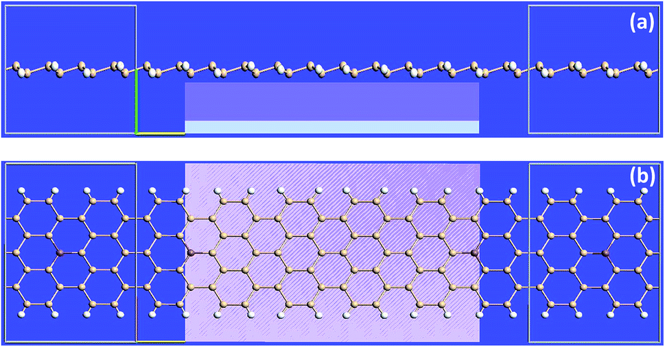
The two-dimensional structure of pristine ASiNR and doped ASiNR devices is designed in the Virtual Nano Lab software package, as shown in Fig. 1(a and b) and Fig. 1(c), respectively.
 |
| | Fig. 1 (a) Top view of a pristine armchair nanoribbon (ASiNR), (b) the front view of an ASiNR, (c) the dopant (pink color) and the change in bond length (δ1, δ2 and δ3) of a doped ASiNR. | |
The geometrical structure of hydrogen passivated pristine ASiNRs and doped ASiNRs is optimized and relaxed up to 0.05 eV Å−1. The ASiNRs show a bulked structure of 0.537 Å and the lattice constants were stabilized at 3.845 Å and 2.286 Å as shown in Fig. 1(a). The Si–Si and Si–H bond lengths are set to be 2.286 Å and 1.1 Å, respectively, and the Si–Xp,n (Xp = Al, Ga, In and Tl for p-type doping and Xn = P, As, Sb and Bi for n-type doping) bond lengths are δ1, δ2, and δ3 = 2.286 Å as shown in Fig. 1(b and c); these values have been previously tested and reported.30 Hence, each dopant does not disturb the planar geometry and bulked structure of the ASiNR. A further device was formed to analyze its transport characteristics, see Fig. 1(b), with two electrode regions (left and right) and a scattering or channel region. In the formation of the device, a width (N = 7, as N is no. of silicon atoms) of 13.9 Å and a channel length of 39.9 Å were used. The doping site is selected to be at the 4th position of the left and right electrodes, and the same position was also selected for the channel region as well. The 4th position (S4) was selected to maintain the symmetry of the ASiNRs along the A and C directions as shown in Fig. 1(c). The total energy and cohesive energy of each doped ASiNR was calculated (see Table 1 in ESI†) which shows that the In doped ASiNR was the best among each of the p-type and n-type doped ASiNRs.
Band gap analysis
The electronic properties of pristine and doped ASiNRs are examined and the band structures of pristine and doped ASiNRs are plotted in Fig. 2. The pristine ASiNRs have a band gap of 0.512 eV, which is similar to that from top previous studies.10,13 The trivalent impurity dopants such as Al, Ga, In and Tl showed p-type semiconducting behavior with band gaps of 0.501, 0.506, 0.510 and 0.510 eV, respectively, as shown in Fig. 2. The pentavalent impurity dopants such as P, As, Sb and Bi showed n-type semiconducting behavior with band gaps of 0.519, 0.522, 0.520 and 0.533 eV, respectively, which are also shown in Fig. 2. In case of the trivalent impurities, the Fermi level is shifted towards the valance band and for pentavalent impurities, the Fermi level is shifted towards the conduction band, as shown in Fig. 2(b–g) (see Table 2 in ESI†). The band structure of each pristine and doped ASiNR confirms that they all have a direct band gap. It is observed that in the case of p-type dopants the band gap is slightly decreased in comparison to those of pristine ASiNRs, whereas in the case of n-type dopants the band gap is increased in comparison to those of ASiNRs. The average decrease in the band gaps of p-type dopants is 1.7% and for n-type dopants the average increase in the band gaps is 2.5% relative to pristine ASiNRs. Hence, p-type dopants reduce the band gap and n-type dopants enhances the band gap. Finally, each doped ASiNR is used as an electrode in the device to achieve negative differential resistance.
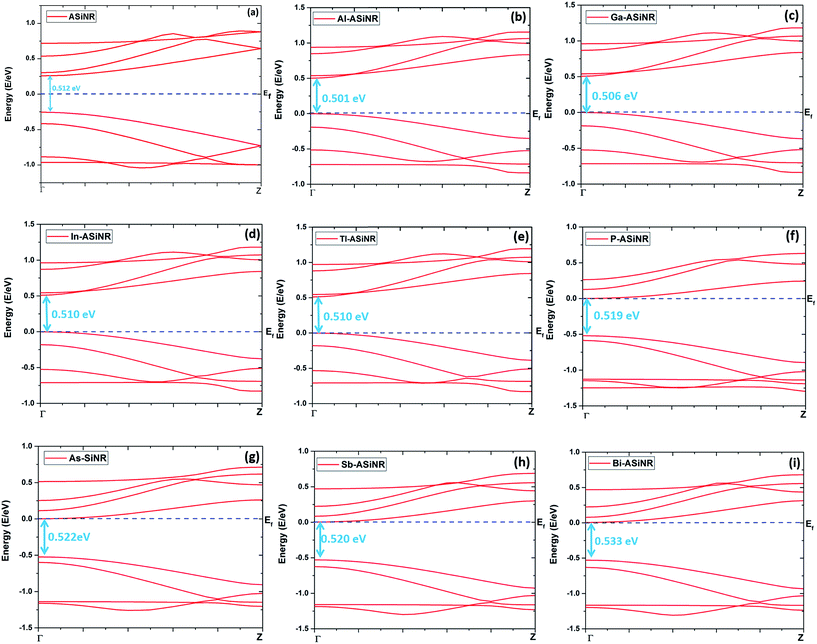 |
| | Fig. 2 Calculated band structure of pristine armchair silicene nanoribbons (ASiNRs) (a), and armchair silicene nanoribbons doped with aluminum (Al-ASiNRs) (b), gallium (Ga-ASiNRs) (c), indium (In-ASiNRs) (d), thallium (Tl-ASiNRs) (e), phosphorus (P-ASiNRs) (f), arsenic (As-ASiNRs) (g), antimony (Sb-ASiNRs) (h) and bismuth (Bi-ASiNRs) (i). The red line shows the available energy band and the blue line represents the Fermi level (Ef). | |
The density of states (DOS) is an essential property to understand the electronic behavior of a material. Therefore, the density of states of ASiNRs and doped ASiNRs is analyzed. The band structure of pristine ASiNRs, DOS = 0 eV−1 at 0 eV, in the range +0.5 to −0.5 eV is observed at the Fermi level as shown in Fig. 3(a). This is due to the band gap being available in pristine ASiNRs. In the case of p-type dopants an appropriate density of states is available due to the shifting of the Fermi level towards the valance band (VB), and the value for the density of states present at the Fermi level is DOS ∼ 12 eV−1 at 0 eV as shown in Fig. 3(b–e). In the case of n-type dopants, a greater density of states is observed in comparison to that for p-type doped ASiNRs, and a value of DOS ∼ 17 eV−1 at 0 eV is observed as shown in Fig. 3(f–i). This can be attributed to the shifting of the Fermi level towards the conduction band (CB). Hence, the size of the dopant results in a minute difference in the DOS and provides a similar value for all of the p-type and n-type dopants. These DOS present at the Fermi level and in the energy range −1 eV to +1 eV will provide a large amount of charge to flow through the electrode region from the source and the drain. The discrete peaks in the DOS will result in the existence of a nonlinear charge flow. Moreover, the wider and higher the width of the DOS peak is for a particular dopant, the higher the number of states available for the charge to flow from the source to the drain. To provide a better analysis of our work we have compared the obtained electronic properties with those from previous reports on similar 2D materials and their one-dimensional (1D) nanoribbons, as shown in Table 1. A comparison of its electronic properties is made by the following parameters: the bond length of unit cell in Angstroms (Å), the band gap in electron volts (eV). Hence, it is clear that graphene, silicene and germenene contain a Dirac point, which provides a band gap of 0 eV, and so they are not suitable for device formation. On the other hand, graphene, germenene and silicene zigzag nanoribbons (ZGNR, ZGeNR and ZSiNR, respectively) also contain a band gap of 0 eV due to both the CB and the VB touching each other at the Fermi level which is responsible for its semi-metallic nature. Hence, only the armchair configurations of graphene, germenene and silicene nanoribbons (AGNRs, AGeNRs and ASiNRs, respectively) have an appropriate band gap of 0.39, 0.54 and 0.51 eV, respectively. Therefore, we have selected ASiNRs because they provide a desirable band gap and they are more feasible with the present silicon based technology in comparison to AGNRs and AGeNRs.
 |
| | Fig. 3 Calculated density of states for pristine armchair silicene nanoribbons (ASiNRs) (a), and armchair silicene nanoribbons doped with aluminum (Al-ASiNRs) (b), gallium (Ga-ASiNRs) (c), indium (In-ASiNRs) (d), thallium (Tl-ASiNRs) (e), phosphorus (P-ASiNRs) (f), arsenic (As-ASiNRs) (g), antimony (Sb-ASiNRs) (h) and bismuth (Bi-ASiNRs) (i). | |
Table 1 A comparison of the electronic properties from the present work on ASiNRs with other reported 2D materials
| Sr. no. |
Material |
Electronic properties |
| Bond length of unit cell (Å) |
Band gap (eV) |
Electronic behavior |
| 1 |
Graphene30,32 |
1.42 |
0 |
Dirac point |
| 2 |
ZGNR33 |
1.43 |
0 |
Semi-metallic |
| 3 |
AGNR34 |
1.43 |
0.39 |
Semi-conducting |
| 4 |
Germenene32 |
2.49 |
0 |
Dirac point |
| 5 |
ZGeNR35 |
∼2.4 |
0.1 |
Semi-metallic |
| 6 |
AGeNR35 |
∼2.4 |
0.54 |
Semi-conducting |
| 7 |
Silicene32 |
2.24 |
0 |
Dirac point |
| 8 |
ZSiNR36 |
2.2 |
0 |
Semi-metallic |
| 9 |
ASiNR10 |
2.28 |
0.49 |
Semi-conducting |
| 10 |
ASiNR (our work) |
2.28 |
0.51 |
Semi-conducting |
Quantum transport
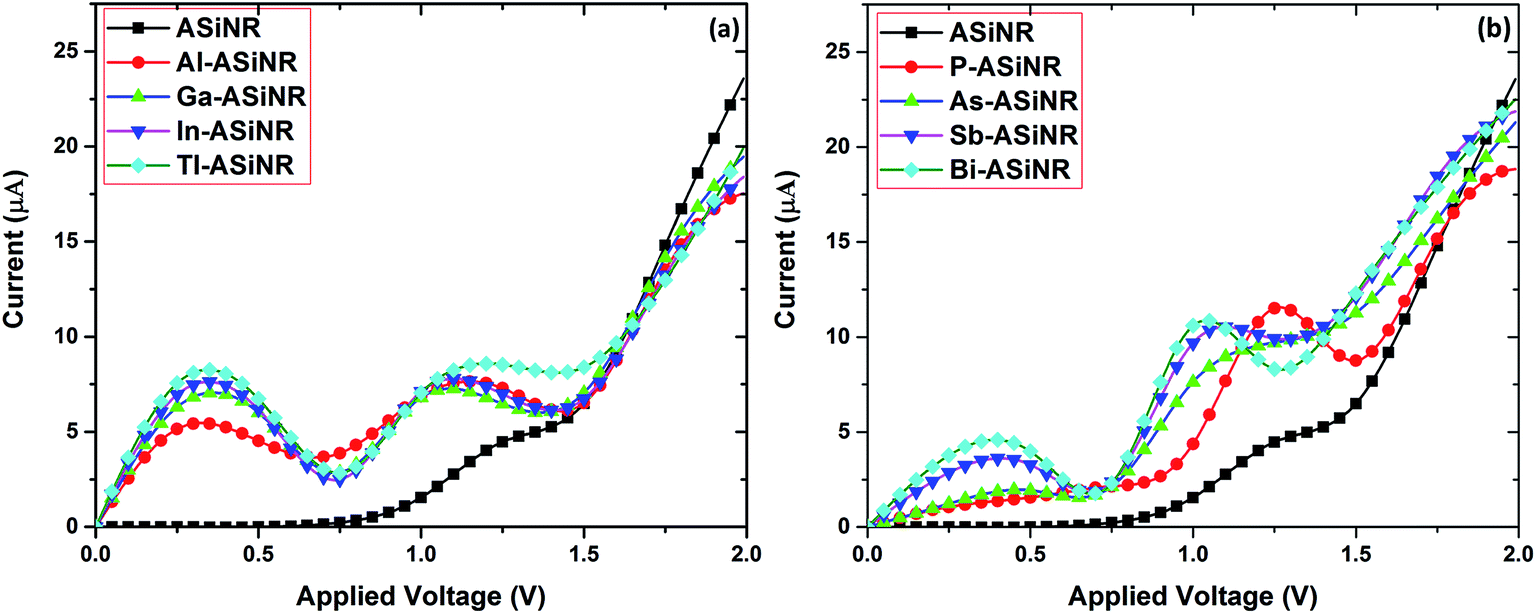
To analyze the quantum charge transport behavior, the device is formed as shown in Fig. 1, then optimized at 300 K electron temperature. The left and right electrodes are both doped with p-type and n-type dopants, and pristine electrodes are also studied to provide a comparison, as shown in Fig. 4(a and b), respectively. A bias voltage is applied from 0 to 2 volts. Firstly, in pristine ASiNRs due to the lack of DOS present at the Fermi level, the current voltage (I–V) characteristics show a threshold of 0.7 eV, beyond which an increase in the current value is observed w.r.t. the applied voltage.37 The absence of NDR is observed in the case of pristine ASiNRs as shown in Fig. 4(a and b) with the black line. Secondly, in the case of p-type dopants, a large amount of NDR is observed with a peak valley ratio (Ip/Iv) for Al, Ga, In and Tl of 1.491, 2.486, 3.091 and 2.908, respectively, as shown in Fig. 4(a). A high value in the DOS at the Fermi level, which is touching the VB, provides a maximum number of allowed states for charge particles to transfer from the source to the drain. When the value of the applied voltage is increased, the value for the present DOS decreases, which provides a smaller or less allowed DOS in comparison to that from when a small applied voltage in each doped ASiNR device is applied. Finally, in the case of n-type dopants a smaller value for NDR is observed due to the Fermi level present at the DOS touching the CB as shown in Fig. 3(f–i). The NDR observed for P, As, Sb and Bi is 1.321, 1.261, 1.972 and 2.617, respectively, as shown in Fig. 4(b). Hence, the current voltage characteristics of p-type dopants in comparison to those from n-type dopants provide a greater value of NDR. From the analysis of each doped ASiNR it is observed that In doped ASiNRs provide the highest value of NDR. In doped ASiNRs are observed to have the best NDR with a maximum value of PVR (see Table 3 in ESI†).
 |
| | Fig. 4 Current voltage (I–V) characterization of (a) pristine armchair silicene nanoribbons ASiNRs (black), and armchair silicene nanoribbons doped with aluminum (Al-ASiNRs) (red), gallium (Ga-ASiNRs) (green), indium (In-ASiNRs) (dark blue) and thallium (Tl-ASiNRs) (light blue), and (b) phosphorus (P-ASiNRs) (red), arsenic (As-ASiNRs) (green), antimony (Sb-ASiNRs) (dark blue) and bismuth (Bi-ASiNRs) (light blue). | |
The NDR behavior of each doped ASiNR structure and the I–V characteristics can be explained by examining the transmission spectra, which are shown in Fig. 5(a and b). The transmission spectra of the p-type and n-type doped ASiNRs along with pristine ASiNRs are shown in Fig. 5(a and b) at 0, 0.5, and 1 V. Firstly, in the case of pristine ASiNRs (black line) no transmission peak is observed in the energy window (dashed blue line) when the applied voltage is 0 or 0.5 V, and so the current value does not rise, but when the applied voltage is further increased, the current value rises from 0.7 eV because of the available transmission peak in the energy window of 1 V as shown in Fig. 5(a). Secondly, in the case of p-type doped ASiNRs the various dopant transmission peaks are also shown in Fig. 5(a). For each p-type doped ASiNR, a similar value of the transmission peak T(E) ∼1.2 and ∼1.5 is observed at 0 V and 0.5 V of applied bias, respectively, and these values are approximately equal in the range of 0.12 eV to −0.25 eV for all of the dopants at 0.5 V. Furthermore, at an applied voltage of 1 V the transmission peaks T(E) for each p-type doped ASiNR are again observed at −0.5 eV and +0.47 eV which cover a similar area under the curve from −0.35 eV to −0.5 eV and from 0.25 to 0.5 eV. Therefore, these transmission peaks in the transmission spectrum provide transmission pathways for the charge carriers at different applied voltages and results in NDR behavior of all of the p-type doped ASiNRs showing similar I–V characteristics. For n-type doped ASiNRs with various dopants, the transmission spectrum possesses a similar transmission value T(E) ∼ 1.2 to the p-type doped ASiNRs at 0 V and T(E) ∼ 1.2 at 0.5 V but this covers a smaller area under the curve from 0.17 eV to 0.25 eV in comparison to that of p-type doped ASiNRs. Further increasing the applied voltage to 1 V, a maximum value of transmission T(E) ∼ 1 is obtained for each n-type doped ASiNR. However, the peak covers a different area under the curves of each dopant with P, As, Sb and Bi covering −0.5 to −0.4 eV, −0.5 to +0.1 eV, −0.5 to +0.1 eV and −0.5 to −0.25 eV, respectively, as shown in Fig. 5(b), due to which the maximum current achieved by each n-type dopant is different, as shown in Fig. 4(b). Therefore, it is observed that p-type doped ASiNRs have a greater transmission value and cover a greater area in comparison to n-type doped ASiNRs at 0 V and 0.5 V and not at 1 V. Finally, NDR behavior is observed in both p-type and n-type doped ASiNRs, which is not a feature of pristine ASiNRs, whereas the p-type dopants show higher NDR in comparison to n-type dopants. The availability of transmission pathways is in agreement with the available density of states in the bias window. We have also compared the transport properties to those of ZGNRs, AGNRs, ZGeNRs, AGeNRs, ZSiNRs and ASiNRs as shown in Table 2. This results in the existence of transmission gaps in the transmission spectra when the applied voltage is 0 V, due to the presence of band gaps in AGNRs, AGeNRs and ASiNRs. Whereas, ZGNRs and ZSiNRs show a transmission value T(E) of 2 and 0.3, respectively. Hence, our present results have a resemblance to those from previous studies at applied low voltages from 0 to 2 V and demonstrate non-linear I–V behavior.
 |
| | Fig. 5 Transmission spectrum at an applied voltage of 0, 0.5 and 1 V for pristine armchair silicene nanoribbons (ASiNRs) (black) (a), and armchair silicene nanoribbons doped with aluminum (Al-ASiNRs) (red), gallium (Ga-ASiNRs) (blue), indium (In-ASiNRs) (green), and thallium (Tl-ASiNRs) (pink), and (b) phosphorus (P-ASiNRs) (red), arsenic (As-ASiNRs) (blue), antimony (Sb-ASiNRs) (green) and bismuth (Bi-ASiNRs) (pink). | |
Table 2 A comparison of the transport properties from the present work on ASiNRs with other reported 2D materials, (—) values not reported
| Sr. no |
Material |
Transport properties |
| Transmission coefficient at 0 V applied voltage (T(E)) |
Current–voltage (I–V) characteristics |
Transport behavior |
| 1 |
ZGNR33 |
2 |
Non-linear |
Ballistic conduction |
| 2 |
AGNR37 |
0 |
Linear |
Transmission gap |
| 3 |
ZGeNR35 |
0 |
— |
Transmission gap |
| 4 |
AGeNR35 |
0 |
— |
Transmission gap |
| 5 |
ZSiNR28,35 |
0.3 |
Non-linear (NDR) |
Non ballistic conduction |
| 6 |
ASiNR (our work) |
0 |
Non-linear (NDR) |
(Transmission gap) |
In doped ASiNR nanotransistor (ASiNR-FET) performance
To determine the performance of ASiNR based devices in the application of nanoelectronics based field effect transistors (FETs), we have studied in detail the interpretation of In doped ASiNR field effect nanotransistors (ASiNR-FETs) as shown in Fig. 6(a and b). The indium (In) doped ASiNR was selected for FET performance testing because it provides the best results for the electronic properties (greatest cohesive energy with an appropriate band gap) and transport properties (NDR with a maximum peak to valley ratio). The device ASiNR-FET structure is optimized as shown in Fig. 6(a) (side view) and Fig. 6(b) (top view) using the high dielectric constant value of lanthanum oxide (La2O3 = 29) at different applied gate voltages (−0.1 to 0.4 V) as shown in Fig. 7(a). The geometry of the ASiNR-FET is optimized and stabilized at 300 K electron temperature. The dimensions of the dielectric and metallic regions are 20 × 4 × 30 nm and 20 × 1 × 30 nm respectively, with a similar configuration for the source and the drain as used in the I–V characteristics part. The contact of the dielectric region to the channel region shifts the peak current and the valley current and is enhanced due to which the Ip/Iv ratio is decreased from 3.091 to 1.639. In Fig. 7(a) it is shown that by varying the VgS from −0.1 V to 0.1 V, Ip is enhanced and Iv is decreased due to which Ip/Iv is increased, and by further varying VgS from 0.2 to 0.4 it is observed that Ip is decreased and Iv is increased which causes a reduction in the Ip/Iv value (see Table 4 in ESI†). The best NDR with the greatest Ip/Iv value is observed at VgS = 0.2 and is 4.603 (blue line). Hence, by applying a gate voltage, we can modulate the Ip/Iv value at each NDR. Secondly, the conductance (G) plot of the In doped ASiNR-FET is also analyzed as shown in Fig. 7(b) at a temperature of T = 0 K and T = 300 K, which proves that its ambipolar nature is comparable to that of the graphene based transistor.38 A Dirac cone is observed at 0.5 V which is due to the p-type doping in the In doped ASiNR-FET. The behaviour of hole conduction in the In doped ASiNR-FET remains unchanged, whereas the behaviour of electron conduction is enhanced in the case of 300 K, comparable to that of 0 K due to a rise in temperature.
 |
| | Fig. 6 (a) Side view of the In doped ASiNR device and (b) the top view of the doped ASiNR device. | |
 |
| | Fig. 7 (a) Current voltage characteristics of the ASiNR device with a constant applied gate voltage from −0.1 to 0.4 V, (b) conductance vs. gate voltage plot at T = 0 K and T = 300 K, (c) transverse characteristics of the ASiNR-FET using a drain current vs. gate voltage plot at VdS = 0.8, 0.9 and 1 V. | |
The transverse curve and FET parameters are calculated to analyze the frequency based performance as shown in Fig. 7(c) and Table 3. The transverse curves are produced at VdS = 0.8, 0.9 and 1.0 V with a varying applied gate voltage (VgS) from −0.2 to 0.4 V, and the Ion/Ioff ratio is 4, 5 and 3, respectively. Each transverse curves show that the FETs have an ambipolar nature, as represented by the conductance plots. Our results for the Ion/Ioff ratio are better than those in the previously reported literature.39 The oscillation and the maximum power consumed by the In doped ASiNR-FET are also computed at a VgS and VdS of −0.1 and 1.0 V, respectively. The maximum power consumed by the In doped ASiNR-FET is defined as Pmax = IdVdS max, the cutoff frequency is fco = gm/2πCgs and the maximum frequency of oscillation is defined as fmax = (fco/2) (gm × Rd)1/2 and is shown in Table 1. The values of transconductance gm (=dId/dVg) and drain resistance Rd (=(dId/dVd)−1) are also shown in Table 3. Our result for the cutoff frequency fco is better than that in previously reported graphene based transistors.40–46 Finally, the comparison between the In doped ASiNR-FET and other 2D materials has been made by presenting the figures of merit (FOM) in Table 4, which shows that the highest Ip/Iv ratio is achieved at room temperature (300 K), with a peak current density of 0.137 μA nm−2. Furthermore, it is interesting that the NDR effect generally appeared within the high bias regions, while the NDR behaviors in the ASiNR-FET are observed at low bias (from 0.0 to 0.7 V), which reduced the power consumption in the device design process.
Table 3 Parameters representing the performances of indium atom doped ASiNR-FET
| In doped ASiNR-FET parameters |
| Maximum power consumed (Pmax) |
5646 nW |
| Cutoff frequency (fco) |
616 GHz |
| Maximum frequency (fmax) |
107 GHz |
| Transconductance (gm) |
12![[thin space (1/6-em)]](https://www.rsc.org/images/entities/char_2009.gif) 236 nΩ−1 236 nΩ−1 |
| Drain resistance (Rd) |
9.874 × 10³ dΩ |
| Gate to source capacitance (Cgs) |
3.163 nF |
Table 4 Comparison of the figures of merit (FOMs) of various NDR values achieved by various 2D materials and the present work, (—) values not reported
| Sr. no. |
Material used as a channel in the field effect transistor |
Performance of the field effect transistor |
| Peak current/valley current (Ip/Iv) |
Peak voltage–valley voltage (|PV–VV|) (in V) |
Peak current |
| 1 |
Nitrogen passivated-graphene47 |
2.7 |
|0.80–0.85| = 0.05 |
1.5 × 10⁷ A cm−2 |
| 2 |
Boron nitride + graphene48 |
1.1 |
|0.40–0.50| = 0.10 |
0.1 (2e2 h−1) |
| 3 |
Graphene45 |
∼1 |
|3.32–3.80| = 0.48 |
— |
| 4 |
Graphene49 |
∼1 |
|1.9–1.5| = 0.40 |
— |
| 5 |
Graphene50 |
2.2 |
0.60 |
1.01 mA μm−1 |
| 6 |
Graphene + boron nitride46 |
1.38 |
0.32 |
0.0153 kA cm−2 |
| 7 |
Silicene20 |
∼1.6 |
|0.3–0.8| = 0.5 |
— |
| 8 |
Our work |
3.091 |
|0.3–0.7| = 0.4 |
0.137 μA nm−2 |
4. Conclusion
In the current work, we present the electronic (band gap and density of states) and transport (I–V characteristics and transmission spectrum) properties of pristine ASiNRs and doped ASiNRs. The ASiNRs having direct band gap semiconducting behavior can effortlessly be modulated to have a p-type and n-type semiconducting nature. The modulation is done by using trivalent impurities (Al, Ga, In and Tl) and pentavalent impurities (P, As, Sb and Bi) as the dopants. The In doped ASiNR is observed to be the second most stable with the highest cohesive energy (−6.0409 eV). In particular, the maximum NDR behavior is observed with Ip/Iv = 3.091. Hence, the device performance of the In doped ASiNR was selected to be analyzed after optimizing its geometrical structure by applying a high dielectric constant value of lanthanum oxide (La2O3 = 29). It is observed that the NDR region of the In doped ASiNR based FET (ASiNR-FET) can be tuned by applying various gate voltages from −0.1 to 0.4 V. It is also observed that the value of PVR is enhanced by a factor of two from VgS −0.1 V to 0.1 V and is reduced by 4.6 times the value. The transverse characteristics are also analyzed to find the Ion/Ioff ratios at different VdS such as 0.8, 0.9 and 1 V these are found to be 4, 5 and 3, respectively, which are also better than those of previously reported FETs.39 Finally, the FET based frequency parameters are also analyzed to detect its potential application in RF oscillators. Our calculated values of In doped ASiNR-FET show better results than those of graphene based FETs, and show that n-type doped ASiNR based FETs can be used in nanoelectronic based devices requiring a modulated or controlled NDR effect, such as in memory devices and RF oscillators.
Acknowledgements
The authors acknowledge funding support from Council of Scientific and Industrial Research, Nanotechnology: Impact on Safety, Health and Environment Program (CSIR-NANOSHE) and Academic support from Central Scientific Instruments Organisation (CSIR-CSIO), Academy of Scientific and Innovative Research (AcSIR). We also acknowledge Rajiv Gandhi National Fellowship (RGNF) for financial support and other group members at CSIO, especially Vandana Gupta, Shriniwas Yadav, Ravi Mehla, Jetinder Kumar, Shashank Sundriyal, Manil Kukkar and Rhishab Kholi for their valuable suggestions and input.
References
- L. Tao, E. Cinquanta, D. Chiappe, C. Grazianetti, M. Fanciulli, M. Dubey, A. Molle and D. Akinwande, Nat. Nanotechnol., 2015, 10, 227–231 CrossRef CAS PubMed.
- G. Le Lay, Nat. Nanotechnol., 2015, 10, 202–203 CrossRef PubMed.
- E. Cinquanta, E. Scalise, D. Chiappe, C. Grazianetti, B. van den Broek, M. Houssa, M. Fanciulli and A. Molle, J. Phys. Chem. C, 2013, 117, 16719–16724 CAS.
- A. Kara, H. Enriquez, A. P. Seitsonen, L. C. Lew Yan Voon, S. Vizzini, B. Aufray and H. Oughaddou, Surf. Sci. Rep., 2012, 67, 1–18 CrossRef CAS.
- D. Zha, C. Chen and J. Wu, Solid State Commun., 2015, 219, 21–24 CrossRef CAS.
- D. Zhang, M. Long, X. Zhang, C. Cao, H. Xu, M. Li and K. Chan, Chem. Phys. Lett., 2014, 616–617, 178–183 CrossRef CAS.
- P. Vogt, P. De Padova, C. Quaresima, J. Avila, E. Frantzeskakis, M. C. Asensio, A. Resta, B. Ealet and G. Le Lay, Phys. Rev. Lett., 2012, 108, 155501 CrossRef PubMed.
- P. Lagarde, M. Chorro, D. Roy and N. Trcera, J. Phys.: Condens. Matter, 2016, 28, 075002 CrossRef CAS PubMed.
- H. Şahin, S. Cahangirov, M. Topsakal, E. Bekaroglu, E. Akturk, R. T. Senger and S. Ciraci, Phys. Rev. B: Condens. Matter Mater. Phys., 2009, 80, 155453 CrossRef.
- S. M. Aghaei and I. Calizo, J. Appl. Phys., 2015, 118, 104304 CrossRef.
- Y. Ding and J. Ni, Appl. Phys. Lett., 2009, 95, 083115 CrossRef.
- P. De Padova, O. Kubo, B. Olivieri, C. Quaresima, T. Nakayama, M. Aono and G. Le Lay, Nano Lett., 2012, 12, 5500–5503 CrossRef CAS PubMed.
- K. Iordanidou, M. Houssa, B. v. d. Broek, G. Pourtois, V. V. Afanas’ev and A. Stesmans, J. Phys.: Condens. Matter, 2016, 28, 035302 CrossRef CAS PubMed.
- Y. C. Cheng, Z. Y. Zhu and U. Schwingenschlögl, EPL, 2011, 95, 17005 CrossRef.
- D. Zhang, M. Long, F. Xie, J. Ouyang, H. Xu and Y. Gao, Sci. Rep., 2016, 6, 23677 CrossRef CAS PubMed.
- N. D. Drummond, V. Zólyomi and V. I. Fal’ko, Phys. Rev. B: Condens. Matter Mater. Phys., 2012, 85, 075423 CrossRef.
- W.-F. Tsai, C.-Y. Huang, T.-R. Chang, H. Lin, H.-T. Jeng and A. Bansil, Nat. Commun., 2013, 4, 1500 CrossRef PubMed.
- L. C. Lew Yan Voon, E. Sandberg, R. S. Aga and A. A. Farajian, Appl. Phys. Lett., 2010, 97, 163114 CrossRef.
- N. Gao, W. T. Zheng and Q. Jiang, Phys. Chem. Chem. Phys., 2012, 14, 257–261 RSC.
- Z. Ni, H. Zhong, X. Jiang, R. Quhe, G. Luo, Y. Wang, M. Ye, J. Yang, J. Shi and J. Lu, Nanoscale, 2014, 6, 7609–7618 RSC.
- Y. Du, J. Zhuang, H. Liu, X. Xu, S. Eilers, K. Wu, P. Cheng, J. Zhao, X. Pi, K. W. See, G. Peleckis, X. Wang and S. X. Dou, ACS Nano, 2014, 8, 10019–10025 CrossRef CAS PubMed.
- A. Lopez-Bezanilla, J. Phys. Chem. C, 2014, 118, 18788–18792 CAS.
- Z.-X. Guo, S. Furuya, J.-i. Iwata and A. Oshiyama, Phys. Rev. B: Condens. Matter Mater. Phys., 2013, 87, 235435 CrossRef.
- J. Zhu and U. Schwingenschlögl, ACS Appl. Mater. Interfaces, 2014, 6, 11675–11681 CAS.
- H. Liu, J. Gao and J. Zhao, J. Phys. Chem. C, 2013, 117, 10353–10359 CAS.
- X.-S. Ye, Z.-G. Shao, H. Zhao, L. Yang and C.-L. Wang, RSC Adv., 2014, 4, 37998–38003 RSC.
- F. Pan, Y. Wang, K. Jiang, Z. Ni, J. Ma, J. Zheng, R. Quhe, J. Shi, J. Yang, C. Chen and J. Lu, Sci. Rep., 2015, 5, 9075 CrossRef CAS PubMed.
- D. Zha, C. Chen, J. Wu and M. Wang, Int. J. Mod. Phys. B, 2015, 29, 1550061 CrossRef CAS.
- C. Cheng, H. Hu, Z. Zhang and H. Zhang, RSC Adv., 2016, 6, 7042–7047 RSC.
- S. Ullah, A. Hussain, W. Syed, M. A. Saqlain, I. Ahmad, O. Leenaerts and A. Karim, RSC Adv., 2015, 5, 55762–55773 RSC.
- H. H. B. Sørensen, P. C. Hansen, D. E. Petersen, S. Skelboe and K. Stokbro, Phys. Rev. B: Condens. Matter Mater. Phys., 2009, 79, 205322 CrossRef.
- P. Miro, M. Audiffred and T. Heine, Chem. Soc. Rev., 2014, 43, 6537–6554 RSC.
- S. Singh, A. D. Sarkar and I. Kaur, Mater. Res. Bull., 2017, 87, 167–176 CrossRef CAS.
- S. Dutta and S. K. Pati, J. Mater. Chem., 2010, 20, 8207–8223 RSC.
- K. Yang, S. Cahangirov, A. Cantarero, A. Rubio and R. D’Agosta, Phys. Rev. B: Condens. Matter Mater. Phys., 2014, 89, 125403 CrossRef.
- L. Yunye, W. Vei, M. Hiroshi and K. Yoshiyuki, J. Phys.: Condens. Matter, 2012, 24, 455302 CrossRef PubMed.
- E. Gracia-Espino, F. Lopez-Urias, H. Terrones and M. Terrones, RSC Adv., 2016, 6, 21954–21960 RSC.
- H. Sadeghi, J. Nanosci. Nanotechnol., 2014, 14, 4178–4184 CrossRef CAS PubMed.
- J. Kedzierski, P. L. Hsu, P. Healey, P. W. Wyatt, C. L. Keast, M. Sprinkle, C. Berger and W. A. D. Heer, IEEE Trans. Electron Devices, 2008, 55, 2078–2085 CrossRef CAS.
- S. K. Gupta and G. N. Jaiswal, Superlattices Microstruct., 2015, 86, 355–362 CrossRef.
- L. Liao, Y.-C. Lin, M. Bao, R. Cheng, J. Bai, Y. Liu, Y. Qu, K. L. Wang, Y. Huang and X. Duan, Nature, 2010, 467, 305–308 CrossRef CAS PubMed.
- Y. M. Lin, C. Dimitrakopoulos, K. A. Jenkins, D. B. Farmer, H. Y. Chiu, A. Grill and P. Avouris, Science, 2010, 327, 662 CrossRef CAS PubMed.
- G. Liu, S. Ahsan, A. G. Khitun, R. K. Lake and A. A. Balandin, J. Appl. Phys., 2013, 114, 154310 CrossRef.
- A. Radoi, M. Dragoman, A. Cismaru, G. Konstantinidis and D. Dragoman, J. Appl. Phys., 2012, 112, 064327 CrossRef.
- Y. Wu, D. B. Farmer, W. Zhu, S.-J. Han, C. D. Dimitrakopoulos, A. A. Bol, P. Avouris and Y.-M. Lin, ACS Nano, 2012, 6, 2610–2616 CrossRef CAS PubMed.
- L. Britnell, R. V. Gorbachev, A. K. Geim, L. A. Ponomarenko, A. Mishchenko, M. T. Greenaway, T. M. Fromhold, K. S. Novoselov and L. Eaves, Nat. Commun., 2013, 4, 1794 CrossRef CAS PubMed.
- W. Qiu, P. D. Nguyen and E. Skafidas, J. Appl. Phys., 2015, 117, 054306 CrossRef.
- Y. Zhao, Z. Wan, X. Xu, S. R. Patil, U. Hetmaniuk and M. P. Anantram, Sci. Rep., 2015, 5, 10712 CrossRef CAS PubMed.
- P. Sharma, L. S. Bernard, A. Bazigos, A. Magrez and A. M. Ionescu, ACS Nano, 2015, 9, 620–625 CrossRef CAS PubMed.
- P. Sharma, L. S. Bernard, A. Bazigos, A. Magrez and A. M. Ionescu, IEEE Electron Device Lett., 2015, 36, 865–867 CrossRef CAS.
Footnote |
| † Electronic supplementary information (ESI) available. See DOI: 10.1039/c6ra27101d |
|
| This journal is © The Royal Society of Chemistry 2017 |
Click here to see how this site uses Cookies. View our privacy policy here. 
 Open Access Article
 This Open Access Article is licensed under a
  ab,
Abir De Sarkarc,
Bijender Singhd and
Inderpreet Kaur
ab,
Abir De Sarkarc,
Bijender Singhd and
Inderpreet Kaur