
 Open Access Article
 This Open Access Article is licensed under a
 Creative Commons Attribution 3.0 Unported Licence
Efficient green electroluminescence based on an iridium(III) complex with different device structures†
Yi-Ming Jinga,
You-Xuan Zheng *abc and
Jing-Lin Zuoa
*abc and
Jing-Lin Zuoa
aState Key Laboratory of Coordination Chemistry, Collaborative Innovation Center of Advanced Microstructures, School of Chemistry and Chemical Engineering, Nanjing University, Nanjing 210093, P. R. China. E-mail: yxzheng@nju.edu.cn
bMaAnShan High-Tech Research Institute of Nanjing University, MaAnShan, 238200, P. R. China
cState Key Laboratory of Luminescence and Applications, Changchun Institute of Optics, Fine Mechanics and Physics, Chinese Academy of Science, Changchun 130033, P. R. China
First published on 12th January 2017
Abstract
A series of phosphorescent organic light-emitting diodes (OLEDs) with single or double light-emitting layer(s) were fabricated using a green iridium(III) complex Ir(BTBP)2POP containing 2′,6'-bis(trifluoromethyl)-2,4′-bipyridine (BTBP) cyclometalated ligand and 2-(5-phenyl-1,3,4-oxadiazol-2-yl)phenol (POP) ancillary ligand. The single light-emitting layer devices with the structure of ITO/MoO3 (5 nm)/TAPC (1,1-bis[4-(di-p-tolylamino)phenyl]cyclohexane, 30 nm)/mCP (N,N′-dicarbazolyl-3,5-benzene, 5 nm)/Ir(BTBP)2POP:PPO21 (3-(diphenylphosphoryl)-9-(4-(diphenylphosphoryl)phenyl)-9H-carbazole, 8 wt%, 10 nm)/TmPyPB (1,3,5-tri(m-pyrid-3-yl-phenyl)benzene, 40 nm)/LiF (1 nm)/Al (100 nm) achieved the highest luminance, current efficiency, power efficiency and external quantum efficiency (EQE) up to 47![[thin space (1/6-em)]](https://www.rsc.org/images/entities/char_2009.gif) 599 cd m−2, 86.5 cd A−1, 52.2 lm W−1 and 31.0%, respectively. Furthermore, the double EML device with the structure of ITO/MoO3 (5 nm)/TAPC (30 nm)/mCP:Ir(BTBP)2POP (8 wt%, 10 nm)/PPO21:Ir(BTBP)2POP (8 wt%, 10 nm)/TmPyPB (40 nm)/LiF (1 nm)/Al (100 nm) obtained a higher maximum luminance of 49139 cd m−2 and slightly lower maximum current efficiency, power efficiency and EQE of 75.8 cd A−1, 51.7 lm W−1 and 27.2%, respectively, with lower turn-on voltage. This research suggested that not only the doping concentration but also the thickness of the emissive and electron transport layers strongly affect the EL performances.
599 cd m−2, 86.5 cd A−1, 52.2 lm W−1 and 31.0%, respectively. Furthermore, the double EML device with the structure of ITO/MoO3 (5 nm)/TAPC (30 nm)/mCP:Ir(BTBP)2POP (8 wt%, 10 nm)/PPO21:Ir(BTBP)2POP (8 wt%, 10 nm)/TmPyPB (40 nm)/LiF (1 nm)/Al (100 nm) obtained a higher maximum luminance of 49139 cd m−2 and slightly lower maximum current efficiency, power efficiency and EQE of 75.8 cd A−1, 51.7 lm W−1 and 27.2%, respectively, with lower turn-on voltage. This research suggested that not only the doping concentration but also the thickness of the emissive and electron transport layers strongly affect the EL performances.
Introduction
Organic light-emitting diodes (OLEDs) have attracted great interest during the last few decades owing to their promising features, including flexibility, color tunability and low power consumption.1 Phosphorescent transition metal complexes have been widely used in OLEDs as the emitter because phosphors can gather both singlet and triplet excitons therefore accomplishing the theoretical 100% internal quantum efficiency.2 Among these complexes, iridium(III) complexes have been intensively studied because of their high phosphorescent quantum efficiency, short lifetime of triplet excited states and broad range of emission colors.3 The strong spin–orbit coupling (SOC) introduced by the central heavy atom can promote the triplet to singlet state radiative transition, which results in extremely high phosphorescence quantum yields at room temperature.However, the device efficiency roll-off ratios of many OLEDs with high efficiency using Ir(III) complexes as the emitter are serious, which is mainly due to the deterioration of charge-carrier balance and increase in nonradiative quenching processes including triplet–triplet annihilation (TTA), triplet–polaron annihilation (TPA), and electric-field-induced dissociation of excitons at high current density.4 In addition, it is well known that the electron mobility of electron transport materials is roughly 2–3 orders of magnitude lower than the hole mobility of most hole transport materials, the efficiency roll-off of devices is dependent on the capability of electron transport. Therefore, that is essential to use bipolar host materials or synthesize Ir(III) complexes with high electron mobility to achieve phosphorescent OLEDs (PhOLEDs) with low efficiency roll-off.
Recently, our group has developed high efficient PhOLEDs using Ir(III) complexes 2′,6′-bis(trifluoromethyl)-2,4′-bipyridine (BTBP) as the main ligand.5 The electron affinity would be increased by the nitrogen heterocycle, while the electron mobility of the complexes may be improved by a more negative framework of ligand C^N such as bipyridine. Moreover, trifluoromethyl unit could enhance the electron mobility and lead to a better balance of charge injection and transfer. The lower vibrational frequency of the C–F bond would reduce the rate of radiationless deactivation. Furthermore, the bulky CF3 substituents could affect the molecular packing, and the steric protection around the metal would suppress the self-quenching behavior.6 In addition, PhOLEDs based on Ir(III) complexes with 1,3,4-oxadiazole derivatives as ancillary ligands also have good performances owing to their high electron mobility, high photoluminescence quantum yield and good thermal/chemical stability.7
In this work, a series of single or double light-emitting layers (EMLs) OLEDs were fabricated with a heteroleptic Ir(III) complex (Ir(BTBP)2POP) using 2′,6′-bis(trifluoromethyl)-2,4′-bipyridine (BTBP) as the main ligand and 2-(5-phenyl-1,3,4-oxadiazol-2-yl)phenol (HPOP) as the ancillary ligand. Finally, efficient green OLEDs with maximum brightness, current efficiency, power efficiency and external quantum efficiency (EQE) up to 47599 cd m−2, 86.5 cd A−1, 52.2 lm W−1 and 31.0%, respectively, was realized by optimizing the doping concentration, the thickness of EML and electron transport layer (ETL).
Results and discussion
OLEDs performance
Device structure and energy level diagram of the OLEDs are depicted in Fig. 1. MoO3 film was deposited upon indium-tin-oxide (ITO) layer as anode modification layer to improve the injection of holes. TAPC (di-[4-(N,N-ditolyl-amino)-phenyl]cyclohexane), which possesses high hole mobility (μh = 1 × 10⁻² cm2 V−1 s−1), was used as hole transport layer (HTL).8 TmPyPB (1,3,5-tri(m-pyrid-3-yl-phenyl)benzene), which possesses low-lying HOMO level (−6.70 eV) and high electron mobility (μe = 1 × 10⁻³ cm2 V−1 s−1), was used as hole block/electron transport layer (HBL/ETL).9 Bipolar PPO21 (3-(diphenylphosphoryl)-9-(4-(diphenylphosphoryl)phenyl)-9H-carbazole) was introduced as the host material (HOMO = −6.21 eV), which has a similar transport capability of holes and electrons (μh = 9 × 10⁻⁶ cm2 V−1 s−1 and μe = 3.0 × 10⁻⁶ cm2 V−1 s−1).4 mCP (N,N′-dicarbazolyl-3,5-benzene) was added as another hole transport layer to lower the HOMO energy barrier between TAPC and PPO21,10 which was also used as the host material in the double EML devices. The molecular structures of materials above are also shown in Fig. 1. | ||
| Fig. 1 Energy level diagram of HOMO and LUMO levels (relative to vacuum level) for materials investigated in this study and their molecular structures. | ||
In our previous report, graded distribution of the HOMO levels of TAPC (−5.50 eV), mCP (−5.90 eV), PPO21 (−6.21 eV) and the LUMO levels of TmPyPB (−2.70 eV), PPO21 (−2.68 eV), mCP (−2.30 eV) is beneficial for the injection and transport of holes and electrons, respectively.11 Thus, balanced distribution of carriers and wide recombination zone could be expected in our device structure. Furthermore, the HOMO and LUMO levels of Ir(BTBP)2POP (−5.58 eV and −2.76 eV, respectively) are within those of PPO21, carrier trapping is conceived to be the dominant EL mechanism of these devices.12
To optimize the doping concentration of Ir(BTBP)2POP, three single EML devices with the structure of ITO/MoO3 (5 nm)/TAPC (30 nm)/mCP (5 nm)/PPO21:Ir(BTBP)2POP (x wt%, 10 nm)/TmPyPB (20 nm)/LiF (1 nm)/Al (100 nm) were fabricated and studied by adjusting x to be 6 (DS1), 8 (DS2), 10 (DS3), respectively. Fig. 2 lists the EL spectra at 8 V, the doping concentration dependence of current density–luminance–voltage, current efficiency–luminance and power efficiency–luminance characteristics of these devices. The EL performances of these devices were summarized in Table 1. From Fig. 2(a) it can be observed that the similarity of the EL and PL (ESI, Fig. S2†) spectra indicates that the EL is caused by emission from the triplet excited states of the iridium complex Ir(BTBP)2POP. The absence of residual emission from PPO21 suggests a complete energy transfer from the host to the dopant in these devices under the electric excitation.
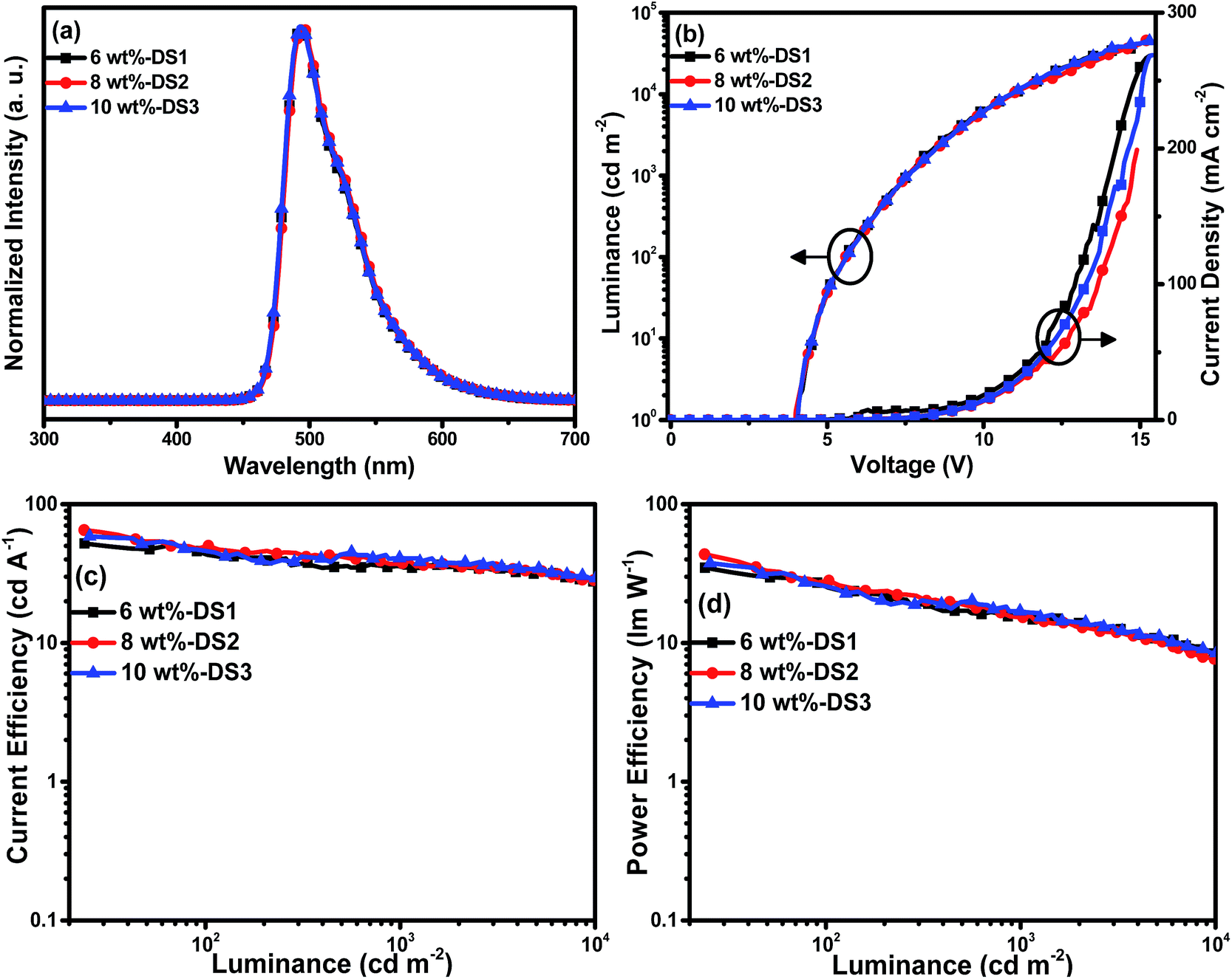 | ||
| Fig. 2 Characteristics of single EML devices with Ir(BTBP)2POP at different doping concentrations: (a) normalized EL spectra at 8 V; (b) current density–luminance–voltage (J–L–V) curves; (c) current efficiency–luminance (ηc–L) curves and (d) power efficiency–luminance (ηp–L) curves. | ||
| Device | Dopant concentration | Vturn-ona (V) | Lmaxb [cd m−2 (V)] | ηc,maxc (cd A−1) (EQEmaxd) | ηc,L1000e (cd A−1) (EQEL1000f) | ηp,maxg (lm W−1) | λmaxh (nm) | CIEi (x, y) |
|---|---|---|---|---|---|---|---|---|
| a Turn-on voltage recorded at a luminance of 1 cd m−2.b Maximum luminance.c Maximum current efficiency.d Maximum external quantum efficiency.e Current efficiency at 1000 cd m−2.f EQE at 1000 cd m−2.g Maximum power efficiency.h Values were collected at 8 V.i Commission Internationale de l'Eclairage coordinates (CIE) at 8 V. | ||||||||
| DS1 | 6 wt% | 4.1 | 36549 (14.7) |
52.1 (18.7%) | 34.9 (12.5%) | 34.8 | 493 | 0.19, 0.54 |
| DS2 | 8 wt% | 4.0 | 45445 (15.2) |
65.1 (23.4%) | 37.6 (13.5%) | 43.5 | 494 | 0.19, 0.55 |
| DS3 | 10 wt% | 4.1 | 44872 (15.3) |
58.7 (21.1%) | 40.7 (14.6%) | 37.6 | 493 | 0.19, 0.54 |
Results suggested that 8 wt% is the optimal concentration of Ir(BTBP)2POP for the single EML devices. As shown in Table 1, the 8 wt% doped device (DS2) achieved the highest luminance, current efficiency, power efficiency and external quantum efficiency (EQE) of 45445 cd m−2, 65.1 cd A−1, 43.5 lm W−1 and 23.4%, respectively. It can also be observed that the turn on voltages of these devices are high (around 4.0 V) though the dopants have good electron mobility, and the charge transport ability of TAPC/TmPyPB is also excellent. One reason is that the carrier mobility of the host material PPO21 is low (μh = 9 × 10⁻⁶ cm2 V−1 s−1 and μe = 3.0 × 10⁻⁶ cm2 V−1 s−1).4 Furthermore, the insertion of mCP would also cause energy loss during the current flow. These two factors may lead to the high turn-on voltages of the devices. Moreover, the efficiency roll-off is somehow apparent, the current efficiency and EQE decreased to 37.6 cd A−1 and 13.5% as the luminance increased to 1000 cd m−2, because of the poor carrier mobility of PPO21.
To further improve the EL performances of Ir(BTBP)2POP, more devices were fabricated by optimizing the thickness of EML and ETL based on the 8 wt% doped single EML device. The EL performances of devices with different thickness of EML or ETL were shown in Fig. 3 and Table 2. From the curves and values in Table 2 it can be observed that the device luminance and efficiency increase firstly to a maximum value and then decrease gradually with increasing thickness of ETL by keeping the thickness of EML constant as 10 nm. The device DS5 with 40 nm ETL achieved the best device performances with maximum luminance, current efficiency, power efficiency and EQE of 47599 cd m−2, 86.5 cd A−1, 52.2 lm W−1 and 31.0%, respectively. With increasing thickness of ETL, the increasing electron transport distance balanced injection and recombination of charge carriers and decreased electron density within EML. As a result, the distribution of holes and electrons tended to balance firstly and then deteriorated gradually when the thickness of ETL was thicker than 40 nm.
 | ||
| Fig. 3 (a) Current density–luminance–voltage (J–L–V), (b) current efficiency–luminance (ηc–L) curves of single EML devices (DS2, DS4–DS7) with different thickness of EML or ETL and (c) current density–luminance–voltage (J–L–V), (d) current efficiency–luminance (ηc–L) curves of single EML device DS5 and double EML device DD1. | ||
| Device | EMLa (nm) | ETLb (nm) | Vturn-onc (V) | Lmaxd [cd m−2 (V)] | ηc,maxe (cd A−1) (EQEmaxf) | ηc,L1000g (cd A−1) (EQEL1000h) | ηp,maxi (lm W−1) |
|---|---|---|---|---|---|---|---|
| a Thickness of EML.b Thickness of ETL.c Turn-on voltage recorded at a luminance of 1 cd m−2.d Maximum luminance.e Maximum current efficiency.f Maximum external quantum efficiency.g Current efficiency at 1000 cd m−2.h EQE at 1000 cd m−2.i Maximum power efficiency. | |||||||
| DS2 | 10 | 20 | 4.0 | 45445 (15.2) |
65.1 (23.4%) | 37.6 (13.5%) | 43.5 |
| DS4 | 10 | 30 | 4.2 | 46743 (16.4) |
82.0 (29.4%) | 49.5 (17.8%) | 51.5 |
| DS5 | 10 | 40 | 4.0 | 47599 (16.5) |
86.5 (31.0%) | 49.2 (17.6%) | 52.2 |
| DS6 | 10 | 50 | 4.0 | 40624 (15.9) |
82.8 (29.7%) | 48.4 (17.4%) | 51.0 |
| DS7 | 15 | 40 | 4.3 | 63954 (19.2) |
83.7 (30.0%) | 51.5 (18.5%) | 37.5 |
| DD1 | — | — | 3.6 | 49139 (13.9) |
75.8 (27.2%) | 43.0 (15.4%) | 51.7 |
Furthermore, the device DS7 with 15 nm EML was also fabricated based on the device DS5. It can be seen that DS7 has higher luminance (63954 cd m−2) and little lower efficiencies (83.7 cd A−1, 37.5 lm W−1 and EQE 30.0%) than that of DS5. The increased thickness of EML caused larger recombination zone and fewer recombination probabilities, within which more dopants were excited to emit but fewer charge carriers recombined, in result of higher luminance and lower efficiencies.
Subsequently, the double EMLs device DD1 with the structure of ITO/MoO3 (5 nm)/TAPC (30 nm)/mCP:Ir(BTBP)2POP (8 wt%, 10 nm)/PPO21:Ir(BTBP)2POP (8 wt%, 10 nm)/TmPyPB (40 nm)/LiF (1 nm)/Al (100 nm) was also fabricated. The EL characteristics of single EML device DS5 and double EML device DD1 are shown in Fig. 3 and Table 2. In most cases, the double EMLs devices will broaden the exciton formation zone, in result of high efficiency and low efficiency roll-off. But compared with DS5, double EML device DD1 obtained a higher maximum luminance of 49139 cd m−2 and lower maximum current efficiency, power efficiency and EQE of 75.8 cd A−1, 51.7 lm W−1 and 27.2%, respectively, and the efficiencies declined obviously as the luminance increased, while the turn-on voltage of 3.6 V was much lower than DS5. The usage of double EML led to the lower charge injection barrier and broadening recombination zone, resulting in the lower turn-on voltage and higher luminance than the single EML device. However, the reduced efficiencies and the high efficiency roll-off were probably due to the poor electron mobility of mCP and PPO21, especially under the high electric field, which would cause the imbalanced injection, transport and recombination of carriers, leading to the lower efficiencies and the high efficiency roll-off.
Experimental section
OLEDs fabrication and measurement
The Ir(BTBP)2POP complex was prepared in our laboratory (ESI†) with emission peak at 503 nm, photoluminescence quantum yield (Φp) of 88%, phosphorescence lifetime (τ) of 2.86 μs in degassed CH2Cl2 solution and HOMO/LUMO levels of −5.58/−2.76 eV in deaerated solution (CH2Cl2:CH3CN = 1:1). All OLEDs with the emission area of 0.1 cm2 were fabricated on the pre-patterned ITO-coated glass substrate with a sheet resistance of 15 Ω sq−1. All chemicals used for devices were sublimed in vacuum (2.0 × 10⁻⁴ Pa) prior to use. The deposition rate for organic compounds is 1–2 Å s−1. The phosphor and host were co-evaporated from two separate sources. The cathode consisting of LiF/Al was deposited by evaporation of LiF with a deposition rate of 0.1 Å s−1 and then by evaporation of Al metal with a rate of 3 Å s−1. The effective area of the emitting diode is 0.1 cm2. The characteristics of the devices were measured with a computer controlled KEITHLEY 2400 source meter with a calibrated silicon diode in air without device encapsulation. On the basis of the uncorrected PL and EL spectra, the CIE coordinates were calculated using a test program of the Spectra scan PR650 spectrophotometer.
Conclusions
In this work, we synthesized a novel heteroleptic Ir(III) complex (Ir(BTBP)2POP) using 2′,6′-bis(trifluoromethyl)-2,4′-bipyridine (BTBP) as the main ligand and 2-(5-phenyl-1,3,4-oxadiazol-2-yl)phenol (HPOP) as the ancillary ligand. A series of devices using Ir(BTBP)2POP as the emitter with single or double EML(s) were fabricated and compared. To balance the distribution of holes and electrons, not only the doping concentration but also the thicknesses of EML and ETL were experimentally optimized. Finally, efficient green device with maximum luminance, current efficiency, power efficiency and EQE up to 47599 cd m−2, 86.5 cd A−1, 52.2 lm W−1 and 31.0%, respectively, was realized. The high efficiency of the device suggests the complex has potential applications in OLEDs.
Acknowledgements
This work was supported by the National Natural Science Foundation of China (21371093, 91433113), the Major State Basic Research Development Program (2013CB922101) and the Natural Science Foundation of Jiangsu Province (BK20130054).Notes and references
- (a) C. W. Tang, S. A. VanSlyke and C. H. Chen, J. Appl. Phys., 1989, 65, 3610 CrossRef CAS; (b) M. A. Baldo, D. F. O'Brien, Y. You, A. Shoustikov, S. Sibley, M. E. Thompson and S. R. Forrest, Nature, 1998, 395, 151 CrossRef CAS; (c) H. Sun, S. Liu, W. Lin, K. Y. Zhang, W. Lv, X. Huang, F. Huo, H. Yang, G. Jenkins, Q. Zhao and W. Huang, Nat. Commun., 2014, 5, 3601 Search PubMed; (d) P. Tao, W. L. Li, J. Zhang, S. Guo, Q. Zhao, H. Wang, B. Wei, S. J. Liu, X. H. Zhou, Q. Yu, B. S. Xu and W. Huang, Adv. Funct. Mater., 2016, 26, 881 CrossRef CAS; (e) K. Y. Zhang, X. Chen, G. Sun, T. Zhang, S. Liu, Q. Zhao and W. Huang, Adv. Mater., 2016, 28, 7137 CrossRef CAS PubMed.
- (a) X. K. Liu, W. C. Chen, H. T. Chandran, J. Qing, Z. Chen, X. H. Zhang and C. S. Lee, ACS Appl. Mater. Interfaces, 2016, 8, 26135 CrossRef CAS PubMed; (b) H. A. Al Attar and A. P. Monkman, Adv. Mater., 2016, 28, 8014 CrossRef CAS PubMed; (c) H. W. Mo, Y. Tsuchiya, Y. Geng, T. Sagawa, C. Kikuchi, H. Nakanotani, F. Ito and C. Adachi, Adv. Funct. Mater., 2016, 26, 6703 CrossRef CAS; (d) R. Gómez-Bombarelli, J. Aguilera-Iparraguirre, T. D. Hirzel, D. Duvenaud, D. Maclaurin, M. A. Blood-Forsythe, H. S. Chae, M. Einzinger, D. G. Ha, T. Wu, G. Markopoulos, S. Jeon, H. Kang, H. Miyazaki, M. Numata, S. Kim, W. Huang, S. I. Hong, M. Baldo, R. P. Adams and A. Aspuru-Guzik, Nat. Mater., 2016, 15, 1120 CrossRef PubMed; (e) Y. H. Zhou, Q. L. Xu, H. B. Han, Y. Zhao, Y. X. Zheng, L. Zhou, J. L. Zuo and H. J. Zhang, Adv. Opt. Mater., 2016, 4, 1726 CrossRef CAS.
- (a) S. Lamansky, P. Djurovich, D. Murphy, F. Abdel-Razzaq, H. E. Lee, C. Adachi, P. E. Burrows, S. R. Forrest and M. E. Thompson, J. Am. Chem. Soc., 2001, 123, 4304 CrossRef CAS PubMed; (b) F. Han, X. Zhang, J. Zhang, Y. Wei, X. Zhang, W. Huang and H. Xu, Chem. Commun., 2016, 52, 5183 RSC; (c) J. X. Cai, T. L. Ye, X. F. Fan, C. M. Han, H. Xu, L. L. Wang, D. G. Ma, Y. Lin and P. F. Yan, J. Mater. Chem., 2011, 21, 15405 RSC; (d) H. Xu, R. Chen, Q. Sun, W. Lai, Q. Su, W. Huang and X. Liu, Chem. Soc. Rev., 2014, 43, 3259 RSC; (e) F. Q. Han, C. M. Han and H. Xu, Chin. Chem. Lett., 2016, 27, 1193 CrossRef CAS.
- W. S. Jeon, T. J. Park, S. Y. Kim, R. Pode, J. Jang and J. H. Kwon, Appl. Phys. Lett., 2008, 93, 063303 CrossRef.
- Q. L. Xu, X. Liang, S. Zhang, Y. M. Jing, X. Liu, G. Z. Lu, Y. X. Zheng and J. L. Zuo, J. Mater. Chem. C, 2015, 3, 3694 RSC.
- Y. Tao, C. Yang and J. Qin, Chem. Soc. Rev., 2011, 40, 2943 RSC.
- (a) H. Y. Li, T. Y. Li, M. Y. Teng, Q. L. Xu, S. Zhang, Y. M. Jin, X. Liu, Y. X. Zheng and J. L. Zuo, J. Mater. Chem. C, 2014, 2, 1116 RSC; (b) Y. M. Jing, C. C. Wang, L. S. Xue, T. Y. Li, S. Zhang, X. Liu, X. Liang, Y. X. Zheng and J. L. Zuo, J. Organomet. Chem., 2014, 765, 39 CrossRef.
- J. Lee, N. Chopra, S. H. Eom, Y. Zheng, J. Xue, F. So and J. Shi, Appl. Phys. Lett., 2008, 93, 123306 CrossRef.
- S. J. Su, T. Chiba, T. Takeda and J. Kido, Adv. Mater., 2008, 20, 2125 CrossRef CAS.
- P. Borsenberger, L. Pautmeier, R. Richert and H. Bässler, J. Chem. Phys., 1991, 94, 8276 CrossRef CAS.
- (a) Q. L. Xu, X. Liang, S. Zhang, Y. M. Jing, X. Liu, G. Z. Lu, Y. X. Zheng and J. L. Zuo, J. Mater. Chem. C, 2015, 3, 3694 RSC; (b) Q. L. Xu, X. Liang, L. Jiang, Y. Zhao and Y. X. Zheng, RSC Adv., 2015, 5, 89218 RSC; (c) Q. L. Xu, X. Liang, L. Jiang, Y. Zhao and Y. X. Zheng, Dalton Trans., 2016, 45, 7366 RSC.
- (a) M. Ikai, S. Tokito, Y. Sakamoto, T. Suzuki and Y. Taga, Appl. Phys. Lett., 2001, 79, 156 CrossRef CAS; (b) M. Uchida, C. Adachi, T. Koyama and Y. Taniguchi, J. Appl. Phys., 1999, 86, 1680 CrossRef CAS.
Footnote |
| † Electronic supplementary information (ESI) available: The synthesis, characterization and properties of the complex. See DOI: 10.1039/c6ra27068a |
| This journal is © The Royal Society of Chemistry 2017 |