
 Open Access Article
 This Open Access Article is licensed under a
 Creative Commons Attribution 3.0 Unported Licence
A non-volatile resistive memory effect in 2,2′,6,6′-tetraphenyl-dipyranylidene thin films as observed in field-effect transistors and by conductive atomic force microscopy†
Marc Courté‡
a,
Sandeep G. Surya‡b,
Ramesh Thamankarc,
Chao Shen a,
V. Ramgopal Raob,
Subodh G. Mhailsalkarde and
Denis Fichou*afg
a,
V. Ramgopal Raob,
Subodh G. Mhailsalkarde and
Denis Fichou*afg
aSchool of Physical and Mathematical Sciences, Nanyang Technological University, 637371, Singapore. E-mail: denisfichou@ntu.edu.sg
bDepartment of Electrical Engineering, Indian Institute of Technology Bombay, Mumbai 400 076, India
cSchool of Engineering and Technology, CMR University, Bangalore 560043, India
dSchool of Material Science and Engineering, Nanyang Technological University, 639798, Singapore
eEnergy Research Institute@NTU (ERI@N), Nanyang Technological University, 637141, Singapore
fCNRS, UMR 8232, Institut Parisien de Chimie Moléculaire, F-75005, Paris, France
gSorbonne Universités, UPMC Univ Paris 06, UMR 8232, Institut Parisien de Chimie Moléculaire, F-75005, Paris, France
First published on 15th December 2016
Abstract
The charge transport properties of 2,2′,6,6′-tetraphenyldipyranylidene (DIPO-Ph4), a large planar quinoïd π-conjugated heterocycle, are investigated in field-effect transistor (FET) configuration and by conductive atomic force microscopy (c-AFM). The FET properties show a clear p-type behavior with a hole mobility up to 2 × 10⁻² cm2 V−1 s−1 and on/off ratio of 104. The transfer characteristics Id/Vg present a clear hysteresis typical of a resistive memory effect. This memory effect is again observed by means of c-AFM in lateral mode using a nearby gold top-contact as the counter-electrode. The c-AFM current response recorded for variable distances d = 0.5–9.0 μm between the AFM tip and the top electrode shows a resistive switching behavior in the low-voltage 0.0–3.0 V region. Repeated “write-read-erase-read” cycles performed at low frequency reveal a non-volatile memory effect in the form of high-resistance and low-resistance states with a stable on/off ratio of 102 during cycling operation.
Introduction
Small-molecule organic semiconductors are intensively investigated in view of applications in electronic devices such as field-effect transistors, photovoltaic solar cells, and light-emitting diodes.1 The ability to tune their electronic properties by chemical design combined with low manufacturing costs and the possibility to implement them on large area and flexible substrates make them attractive as alternatives to silicon and other inorganic materials. Small π-conjugated organic molecules also emerge as good candidates for organic memory devices (OMDs).2 In addition to the above-mentioned advantages inherent to organic materials, OMDs can operate at low voltages (typically below 3 V),3 possess high switching ratios,4 allow miniaturization down to the nanoscale as well as multiple memory states toward high density storage.5 Therefore, OMDs can potentially find applications in future non-volatile memory technologies such as data-storage components in logic circuits.The first memory effect in a molecular material has been observed in the early 70's in anthracene and pentacene.6 Since then, several types of OMDs based on small organic molecules and polymers have been investigated. Examples of small molecules that have been integrated into OMDs over the past fifteen years are sexithiophene,7 linear ethynylphenyl-1-benzenethiolates,8 rose bengal,9 dicyano-1,4-benzoquinone,10 and a polychlorotriphenylmethyl radicals,11 among others.12 While polymer-based OMDs are generally prepared from a mixture of organic polymers sandwiched between two electrodes, molecular OMDs mostly consist in a monolayer of organic material.7,13 Recently, inorganic nanoparticles made of metals, insulators or semiconductors, have been integrated into the organic layer of OMDs resulting in higher memory performance.14 The origin of the resistive effect can be found in the intrinsic properties of the active organic material. Various mechanisms have been proposed to explain electrical bistability such as filament conduction, space charge and traps, charge transfer effects and conformational changes.15 Finally, it is worth noting that the operation mechanism of graphene-based non-volatile ReRAM devices has been recently reviewed.16
OMDs can be made of a simple layer of active material sandwiched between top and bottom electrodes but are generally based on a three-terminal architecture such as a field-effect transistors (FET).7,12 However, other techniques such as conductive atomic force microscopy (c-AFM) are also used to investigate and understand the origin of a memory effect. For example, Jung et al. recently revealed using c-AFM that an irreversible current path has formed near particles that have been inserted in a polymer film and that particle-insertion is a promising method for fabricating low-cost and air-stable “write-once-read-many-times” memories.17 Besides, Pham et al. observed by means of c-AFM that resistive switching in Cr2O3 films occurs as a result of Ag filament paths leading to a large memory density of 100 Tbit per sq. inch with a small filament diameter of 2.9 nm.18 Finally, Wang et al. have been using electrostatic force microscopy (EFM) and Kelvin probe force microscopy (KPFM), two other local-probe techniques, to visualize the charge trapping behavior of the dumbbell-shaped organic molecule 1,6-di(spiro[fluorene-9,90-xanthene]-2-yl)pyrene. These authors demonstrate that the application potential of this organic semiconductor in non-volatile memory devices arises from its outstanding charge storage properties.19
The 2,2′,6,6′-tetraphenyldipyranylidene (DIPO-Ph4, Scheme 1) consists in two pyranylidene heterocycles that are linked together by an exocyclic C![[double bond, length as m-dash]](https://www.rsc.org/images/entities/char_e001.gif) C double bond in para-position relative to the O-atom.20 The quinoïdal structure of the dipyranylidene core is reminiscent of the well-known tetrathiafulvalene (TTF), and acts as well as an excellent π-donors with potential applications in molecular electronics.21 For example, its sulfur analogue 2,2′,6,6′-tetraphenylthiapyranylidene has been used as an efficient hole transporting/electron blocking interfacial layer in organic solar cells.22 Here we study the electrical properties of vacuum-deposited thin films of 2,2′,6,6′-tetraphenyl-dipyranylidene in field-effect transistor configuration and by means of c-AFM (Scheme 2). For both configurations, the I–V characteristics reveal the presence of a clear counter-clockwise hysteresis. Using c-AFM ability and top contact electrode, we could measure in lateral mode the current–voltage response at a micrometric distances d = 0.5–9.0 μm shorter than our FET channel lengths L = 75–200 μm. Current–voltage curves reveal a clear resistive effect in the low-voltage 0.0–3.0 V region. Repeated “write-read-erase-read” cycles performed at low frequency are typical of a non-volatile memory effect in the form of high and low resistance states. The conduction mechanism obeys a space-charge limited conduction (SCLC) arising from charge trapping.
C double bond in para-position relative to the O-atom.20 The quinoïdal structure of the dipyranylidene core is reminiscent of the well-known tetrathiafulvalene (TTF), and acts as well as an excellent π-donors with potential applications in molecular electronics.21 For example, its sulfur analogue 2,2′,6,6′-tetraphenylthiapyranylidene has been used as an efficient hole transporting/electron blocking interfacial layer in organic solar cells.22 Here we study the electrical properties of vacuum-deposited thin films of 2,2′,6,6′-tetraphenyl-dipyranylidene in field-effect transistor configuration and by means of c-AFM (Scheme 2). For both configurations, the I–V characteristics reveal the presence of a clear counter-clockwise hysteresis. Using c-AFM ability and top contact electrode, we could measure in lateral mode the current–voltage response at a micrometric distances d = 0.5–9.0 μm shorter than our FET channel lengths L = 75–200 μm. Current–voltage curves reveal a clear resistive effect in the low-voltage 0.0–3.0 V region. Repeated “write-read-erase-read” cycles performed at low frequency are typical of a non-volatile memory effect in the form of high and low resistance states. The conduction mechanism obeys a space-charge limited conduction (SCLC) arising from charge trapping.
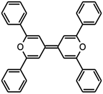 | ||
| Scheme 1 Chemical structure of 2,2′,6,6′-tetraphenyl-dipyranylidene (DIPO-Ph4). | ||
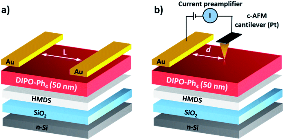 | ||
| Scheme 2 (a) A DIPO-Ph4 based field-effect transistor (L = 75–200 μm) and (b) c-AFM configuration used to measure the memory effect. During c-AFM recording, the Pt cantilever is biased with respect to the DIPO-Ph4 sample surface and positioned at various distances (d ≈ 0.5–9.0 μm) from the gold electrodes. | ||
Results and discussion
Thin films characterization
DIPO-Ph4 thin films are prepared by vacuum deposition on silicon (100) wafers which are modified beforehand with a HMDS thin film layer in order to improve the interface dielectric/organic. Scanning electron microscope (SEM) image deposited on HMDS modified silicon wafer reveals a uniform surface with no pinholes as compared to DIPO-Ph4 films deposited directly on silicon wafer (Fig. S1†). The topography AFM images show an homogenous surface composed of monodisperse grains with a root mean square (RMS) roughness of 11.2 nm (Fig. 1a). A distribution of the number of grains in function of their height shows an average height around 50 nm, the highest grains reaching 80 nm (Fig. 1d). Topography and current-sensing AFM images recorded simultaneously on the silicon substrate (Fig. 1b and c) highlight intense hole-transporting pathways with current intensities up to 161 pA under a −0.1 V applied tip voltage.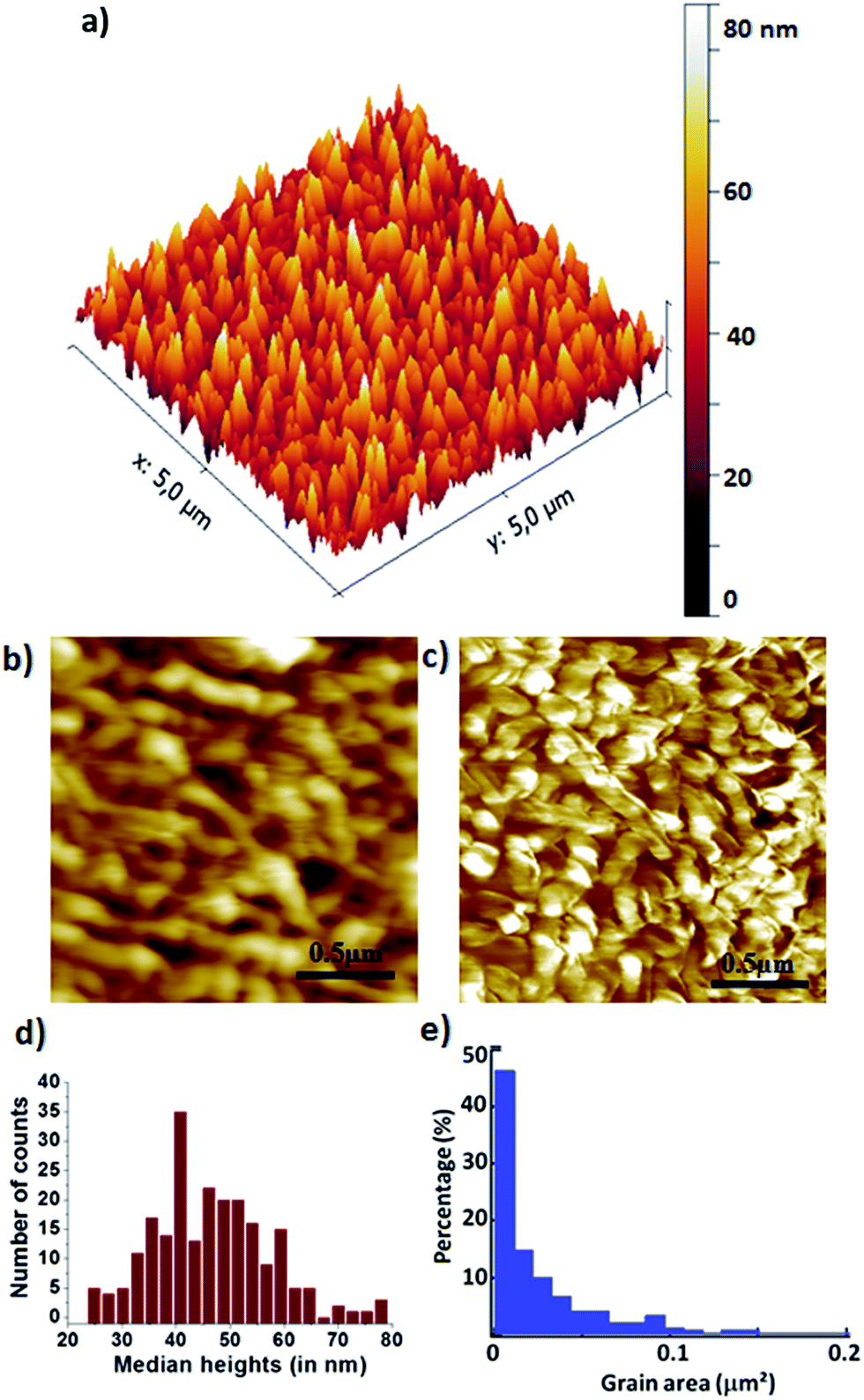 | ||
| Fig. 1 (a) 3D lateral view of an AFM image (5 × 5 μm2) recorded in tapping-mode of a 50 nm DIPO-Ph4 thin film vacuum-deposited on a Si/SiO2/HMDS wafer. (b) Topological AFM image (2 × 2 μm2) and (c) corresponding conductive AFM current mapping of a DIPO-Ph4 film recorded under a −0.1 V tip voltage (current intensities are in the range 0–161 pA). (d) Median height grain distribution and (e) grain surface area distribution, extracted from a typical AFM image. | ||
These conducting pathways are distributed over the whole sample area (bright areas in Fig. 1c). The exceptional hole-carrying behavior of our polycrystalline DIPO-Ph4 thin films constitute a strong basis in view of device applications.
Besides, X-ray diffraction (XRD) performed on DIPO-Ph4 films (50 nm) shows an intense peak at 8.92° (Fig. 2, left), leading to a d-spacing of 9.12 Å as calculated using the Bragg law. On the other hand, X-ray analysis of DIPO-Ph4 single crystals shows that the molecular length is 11.92 Å (Fig. S2†). X-ray diffraction of DIPO-Ph4 single crystals also reveals that it crystallizes in a monoclinic system where the DIPO-Ph4 molecules are packed face-to-face in a herringbone fashion. The combination of both types of X-ray analysis (thin film and single crystal) reveals that in our polycrystalline vacuum-deposited thin films the long axis of the DIPO-Ph4 molecules form a tilt angle of 41° with the substrate plane (Fig. 2, right). The face-to-face molecules have a intermolecular distance of d = 3.5 Å, typical of a π-stacking arrangement. However along the x∥ axis, the minimal intermolecular distance between pyran heterocycles is d = 7.6 Å.
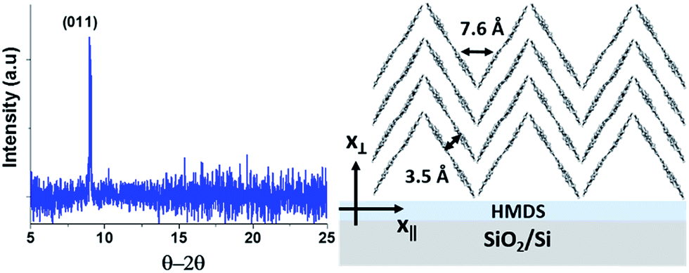 | ||
| Fig. 2 Left: Typical XRD pattern of a polycrystalline DIPO-Ph4 thin film (50 nm) vacuum-deposited on HMDS-treated SiO2/Si substrates. Right: Molecular packing of DIPO-Ph4. The intermolecular distances are measured between two neighboring pyran heterocycles. | ||
Field-effect transistors
Transport properties of DIPO-Ph4 film are investigated in a field-effect transistor configuration. The output and transfer characteristics performed on bottom-gate/bottom-contact OFET devices show a typical p-type behavior (Fig. S3†). After annealing at 200 °C, the carrier mobility is as high as 2 × 10⁻² cm2 V−1 s−1 with an on/off current ratio of 6 × 10⁴. The OFET characteristics before and after annealing at 150 °C and 200 °C are summarized in Table 1.| Annealing temperature (°C) | Mobility (cm2 V−1 s−1) | On/off ratio | Subthreshold voltage (V per decade) | Threshold voltage (V) |
|---|---|---|---|---|
| No annealing | 6.2 × 10⁻³ | 2.8 × 10³ | −16.2 | 7.5 |
| 150 | 9.1 × 10⁻³ | 1 × 10⁴ | −9.1 | −0.5 |
| 200 | 0.02 | 6.2 × 10⁴ | −4.6 | −7.5 |
Moreover, the threshold voltage is shifted from 7.5 V towards −7.5 V and the subthreshold voltage is reduced to −4.6 V per decade which indicates a higher degree of crystallinity of the organic film. Forward and reverse scans of the output and transfer curves of the corresponding DIPO-Ph4-based OFETs have been investigated (Fig. 3).
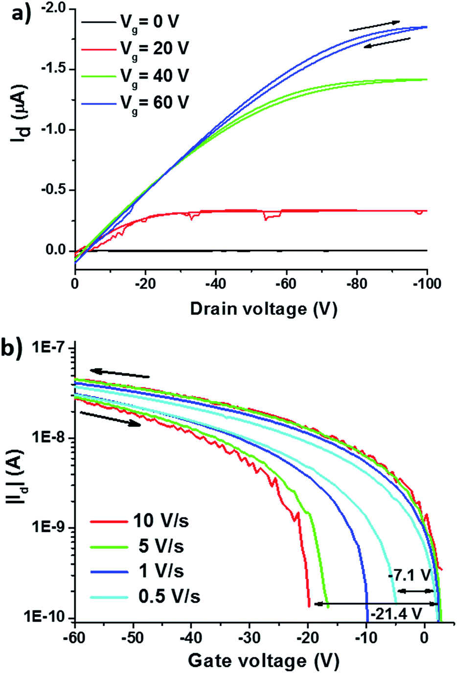 | ||
| Fig. 3 (a) Output Id/Vd curves of a DIPO-Ph4 based FET (L = 200 μm). (b) Transfer curves of the corresponding DIPO-Ph4-based OFET measured at different scan rate (0.5; 1; 2; 5; 10 V s−1) with forward and reverse scans (Vds = 0 V). The arrows indicate the direction of the voltage sweep. | ||
For all samples, the transfer curves present a clear counter-clockwise hysteresis. The hysteresis windows VTh = VTh,reverse − VTh,forward is evaluated as a function of the scan rate (Fig. 3b). At a fast scan rate of 10 V s−1, the hysteresis window is going up to −20.7 V, whereas at a slow scan rate of 0.5 V s−1, the window is reduced to −7.1 V. Such a hysteresis is generally observed in the presence of a dielectric or ferroelectric layer inserted between the organic layer and the oxide layer.
Memory effect measured by c-AFM
The DIPO-Ph4 thin films are deposited on silicon substrates and analyzed by c-AFM in order to investigate further the memory effect observed in OFETs. In contrast to vertical memory devices such as a field-effect transistor, c-AFM allows to record I/V curves in a lateral geometry, the system being then {AFM cantilever/DIPO-Ph4 film/Au}. Using c-AFM brings two advantages over vertical structures: (i) the c-AFM tip contact is non-destructive for the organic film as compare to a metal-deposited contact, (ii) I/V curves can be recorded on the same sample at various electrode separation distances d. In this measurement, the c-AFM cantilever is positioned precisely on the film at various distances d = 0.5–9.0 μm from the gold electrode (Scheme 2b). When an external voltage ranging from +3 V to −3 V is applied, the devices generate a current as high as ≈10 nA (Fig. 4). At positive voltages up to +3 V, the recorded current is reversible. In contrast, for negative voltages down to −3 V, that is when electron injection is coming from the gold electrode, a strong current hysteresis is observed. Such a hysteresis in the I/V curves is observed for all distances d. However, for distances less than one micrometer, the close proximity of the two electrodes does not allow to observed a clear and reproducible hysteresis. The most accentuated hysteresis has been recorded for a distance d = 5.5 μm, with the larger current ratio (≈7.5 nA at −2.5 V) between both voltage sweeps. We have been using this distance d = 5.5 μm to perform the forthcoming measurements (Fig. 5).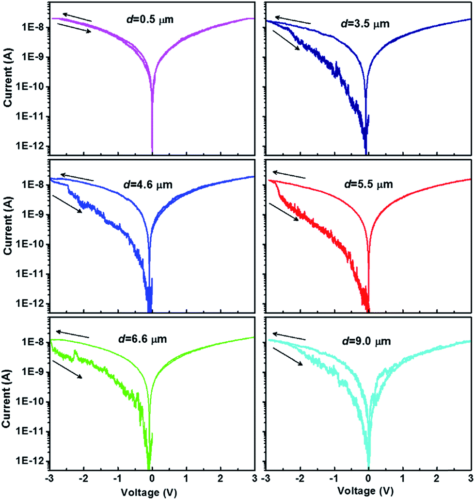 | ||
| Fig. 4 Typical I–V characteristics of a DIPO-Ph4 thin film using c-AFM. The c-AFM cantilever is successively positioned at various distances d from the gold electrode (see Scheme 2). The arrows indicate the voltage sweep direction. | ||
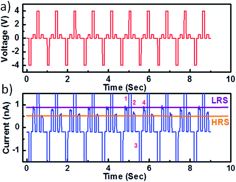 | ||
| Fig. 5 (a) Voltage profile (between +4 V and −4 V) as applied to the DIPO-Ph4 thin film (50 nm) during c-AFM memory measurements. (b) Current response during 10 “write-read-erase-read” voltage cycles. Label 1 indicates the “write” cycle (+4 V) whereas label 3 is for the “erase” cycle (−4 V). Labels 2 and 4 indicate the “read” cycle measured at +0.5 V. The orange line represents the high resistance state (HRS) whereas the purple line represents the low resistance state (LRS) of the memory device. | ||
This I–V hysteresis can be used to operate a memory device. Therefore, we recorded the “write-read-erase-read” voltage cycles at low frequency (1 Hz) on the DIPO-Ph4 sample still using the c-AFM cantilever (Fig. 4a). Initially a +4 V pulse is applied as a “write” pulse to switch the device from a low-resistance state (LRS, horizontal purple line in Fig. 3b) to a high-resistance state (HRS, horizontal orange line). Then by applying +0.5 V the current can be “read” in the device corresponding to HRS. This state can be “erased” by applying a −4 V pulse to get the device back to a low resistance state (LRS). Further, this state is “read” again by applying a +0.5 V pulse, giving rise to a higher current state of the device. During the “read” step of the second cycle, a reduction in current is observed which is attributed to a decrease in the effective voltage due to the screening of the injected charges by the DIPO-Ph4 layer. Moreover, the current does not return back to zero when the applied voltage decreases down to 0 V. These read-write-erase-read measurements clearly indicates that the lateral DIPO-Ph4 based memory devices satisfy the necessary conditions for binary storage devices and present a potential for operating in non-volatile memory. To complete the memory effect measurement, the endurance test was performed by measuring current at a constant applied voltage stress. Current was read continuously up to 103 cycles and a stable on/off ratio of ≈102 up to 1000 s (Fig. 6).
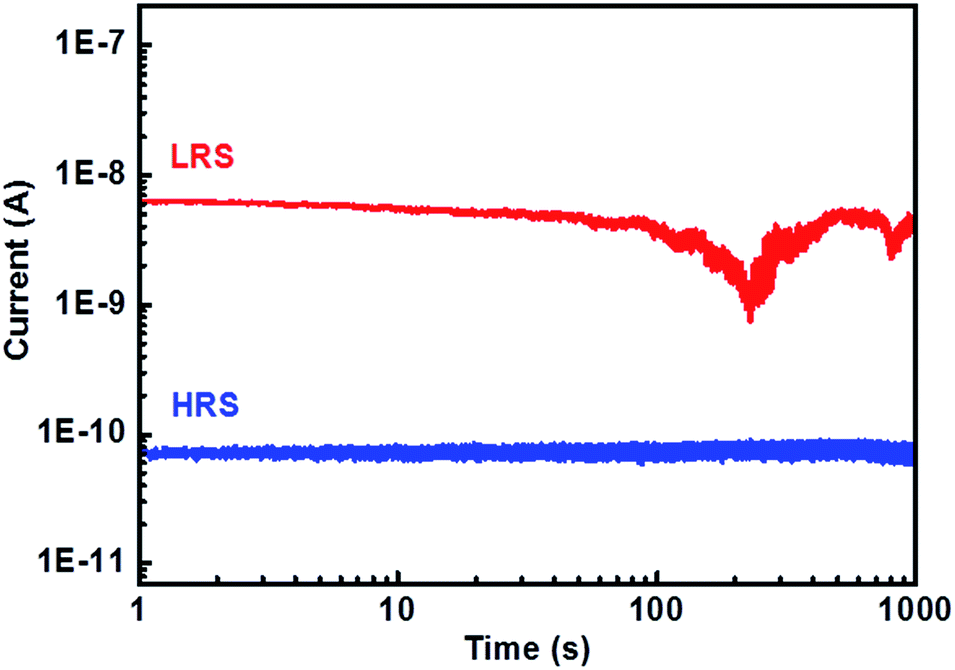 | ||
| Fig. 6 Time-dependence of the c-AFM current of a DIPO-Ph4 thin film recorded at −4 V and −0.5 V respectively over the first 1000 seconds. The LRS (red) and HRS (blue) states are clearly observed with an on/off ratio of 102. The current instability observed in the 100–1000 seconds range of the LRS signal is generated by the voltage reset that has to be done every 200 seconds due to instrumental limitation inherent to our AFM setup. | ||
The conduction mechanism of the DIPO-Ph4 memristor have been analyzed by the log–log I–V curves for positive and negative bias voltage (Fig. 7). For positive voltage sweep, the current curve is proportional to the voltage I ∝ V, thus indicating a strictly ohmic conduction. When the voltage is swept toward negative values, the current conduction remains ohmic. However, when the voltage is swept back the current is proportional to I ∝ V2 showing that it obeys a space-charge limited conduction (SCLC). This SCLC regime could be interpreted in term of charge diffusion inside the DIPO-Ph4 thin film. Charge transport in organic semiconductor generally takes place in the form of hopping mechanism and it is heavily dependent of the molecular packing. X-ray diffraction performed on DIPO-Ph4 (Fig. 2) reveals a herringbone arrangement which will result in a charge transport anisotropy. Transport will be more effective along the vertical x⊥ axis due to π-stacking between neighboring molecules with an intermolecular distance of 3.5 Å. In contrast, along the horizontal x∥ axis the intermolecular distance is larger and not constant. The poor intermolecular overlapping will hinder the charge carrier transport. In addition, the morphology of the DIPO-Ph4 thin films is polycrystalline thus favoring charge trapping at grain boundaries. Indeed, preliminary measurements using time-resolved optical spectroscopy substantiate the presence of a high number of trapped excitons inside the DIPO-Ph4 thin film.
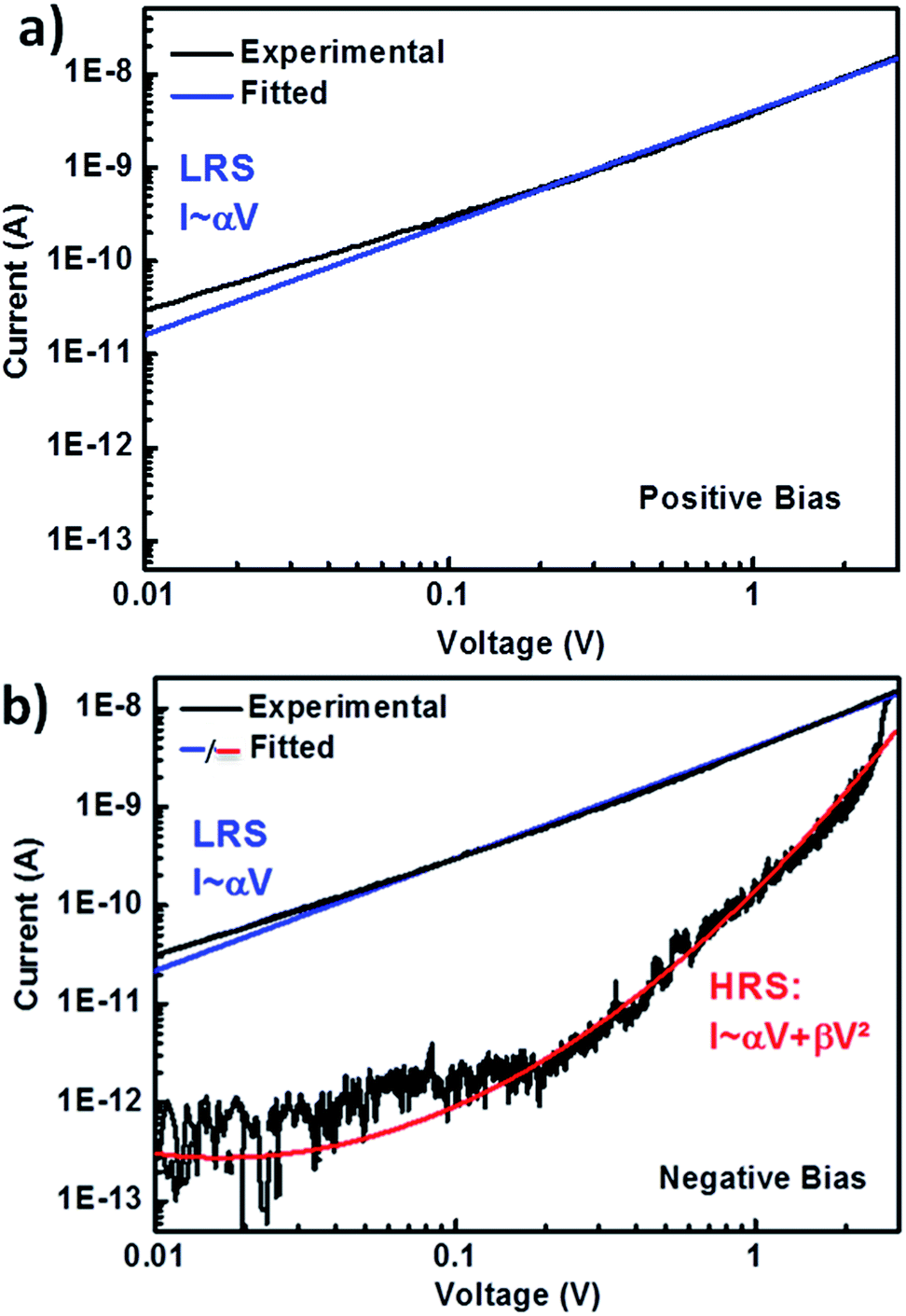 | ||
| Fig. 7 log–log I–V curves for (a) positive voltage sweep and (b) negative voltage sweep of a DIPO-Ph4 thin film where the cantilever is positioned at 5.5 μm from gold electrode. Blue and red curves represent the fitted curves of low resistance state (LRS) and high resistance state (HRS) respectively. | ||
Conclusions
In summary, we report here the charge transport properties of 2,2′,6,6′-tetraphenyldipyranylidene thin films in a field-effect transistor configuration and by conductive atomic force microscopy. The FET properties show a clear p-type behaviour with a hole mobility up to 2 × 10⁻² cm2 V−1 s−1 and on/off ratio of 104. The transfer curves present a clear counter-clockwise hysteresis typical of a resistive memory effect. By means of conductive-AFM, the first observation of a memory effect in DIPO-Ph4 thin films are observed. The I–V characteristics recorded along various distances of a few microns (d = 0.5–9.0 μm) between the AFM tip and the top gold electrode reveal a distinct memristor behaviour when the voltage is swept toward negative bias as compare to the positive voltage sweep. This hysteresis is typical of a non-volatile memory effect in the form of high and low resistance states which are revealed using “write-read-erase-read” cycles. The memory effect is characterized by a stable on/off ratio of 102 up to 1000 s. The memristor behaviour arises from a space-charge-limited-conduction probably due to charge trapping in the DIPO-Ph4 thin film. We are now focusing on the elaboration of DIPO-Ph4 based memory device integrating a dielectric layer in order to improve the memristor properties.Experimental section
Synthesis
The details of the synthesis of DIPO-Ph4 are reported in ESI (ESI, Scheme S1†). In short, DIPO-Ph4 is prepared in a three-step process from glutaryl chloride which is preliminarily functionalized with two phenyl groups using a Friedel–Craft acylation, and further oxidized by BF4·Et2O into a pyrylium salt. The latter compound is then reduced by tributylphosphine P(C4H9)3. The intermediate ylide is finally condensed in basic medium to form DIPO-Ph4. The raw product is a red powder that is purified by Soxhlet extraction in order to obtain high purity compound. The final compound is a highly crystalline deep red material with shiny metallic reflections.Thin film morphology
DIPO-Ph4 molecules are evaporated at a slow rate of 0.2 Å s−1 under high vacuum (P ≈ 10−4 Pa) monitored by a quartz microbalance (Inficon, X TM/2) on single sided n-type low resistivity (0.01–0.02 Ω cm−2) Si (100) wafers (Silicon Valley Microelectronics, SVM) with a 300 nm thick SiO2 grown on top using dry oxidation. Before usage, the substrates were sonicated using ethanol, acetone and isopropyl alcohol for 10 minutes each and treated by UV-ozone for 15 minutes. Hexamethyldisilazane (HMDS, Sigma-Aldrich, >99%) was spin-coated on top of SiO2 at 3000 rpm for 60 seconds and annealed at 100 °C for 10 minutes. The morphology of vacuum-deposited DIPO-Ph4 films (50 nm) is analyzed by AFM (Bruker, Dimension V) and scanning electron microscopy (Jeol, JSM-6700F).Field-effect transistors
FET devices were fabricated in top contact configuration by deposition of 85 nm gold layer through a metallic mask leading to a channel width W = 4000 μm and different channel lengths L = 75, 100, 125, 150, 175 and 200 μm (Scheme 2a). The FET characteristics are recorded under inert atmosphere using a probe-station (Anexus) and a source-meter (Agilent, B2902A).Conductive AFM
The memory effect is recorded on FET and by c-AFM in lateral mode. Gold pads deposited on top of the DIPO-Ph4 films are used as primary electrodes and the AFM tip (Pt, Rocky Mountain Nanotechnology) plays the role of a second electrode. The Pt cantilever is biased with respect to the DIPO-Ph4 sample surface and positioned at various distances d = 0.5–9.0 μm from the gold electrode (Scheme 2b). All AFM measurements are carried out at room temperature and images are processed and analyzed using the software WSXM 5.0.23Acknowledgements
The authors wish to thank the support from the Ministry of Education in Singapore under the AcRF Tier 2 (MOE2014-T2-1-132) and the Nanyang Technological University for a Start-Up Grant.Notes and references
- (a) A. Mishra and P. Bauerle, Angew. Chem., Int. Ed., 2012, 51, 2020–2067 CrossRef CAS PubMed; (b) C. L. Wang, H. L. Dong, W. P. Hu, Y. Q. Liu and D. B. Zhu, Chem. Rev., 2012, 112, 2208–2267 CrossRef CAS PubMed; (c) S. P. Tiwari, E. B. Namdas, V. R. Rao, D. Fichou and S. G. Mhaisalkar, IEEE Electron Device Lett., 2007, 28, 880–883 CrossRef CAS; (d) Y. Lin and X. Zhan, Acc. Chem. Res., 2016, 49, 175–183 CrossRef CAS PubMed; (e) J. E. Coughlin, Z. B. Henson, G. C. Welch and G. C. Bazan, Acc. Chem. Res., 2014, 47, 257–270 CrossRef CAS PubMed; (f) J. Roncali, Acc. Chem. Res., 2009, 42, 1719–1730 CrossRef CAS PubMed; (g) M. C. Gather, A. Köhnen and K. Meerholtz, Adv. Mater., 2011, 23, 233–248 CrossRef CAS PubMed; (h) D. Fichou, G. Horowitz, Y. Nishikitani, J. Roncali and F. Garnier, Synth. Met., 1989, 28(1–2), 729–734 CrossRef.
- (a) D. Prime and S. Paul, Philos. Trans. R. Soc., A, 2011, 367, 4141–4157 CrossRef PubMed; (b) C. Wang, P. Gu, B. Hu and Q. Zhang, J. Mater. Chem. C, 2015, 3, 10055–10065 RSC; (c) B. Cho, S. Song, Y. Ji, T. W. Kim and T. Lee, Adv. Funct. Mater., 2011, 21, 2806–2829 CrossRef CAS.
- A. Nougaret, H. G Kassa, R. Cai, T. Patois, N. Nysten, A. J. J. M van Breemen, G.-H. Gelinck, D. M. de Leeuw, A. Marrani, Z. Hu and A. M. Jonas, ACS Nano, 2014, 8, 3498–3505 CrossRef PubMed.
- C. S. Smithson, Y. Wu, T. Wigglesworth and S. Zhu, Adv. Mater., 2015, 27, 228–233 CrossRef CAS PubMed.
- (a) T. Leydecker, M. Herder, E. Pavlica, G. Bratina, S. Hecht, E. Orgiu and P. Samorì, Nat. Nanotechnol., 2016, 11, 769–775 CrossRef CAS PubMed; (b) L. Li and D. Wen, Org. Electron., 2016, 34, 12–17 CrossRef CAS.
- (a) J. Kevorkian, M. M. Labes, D. C. Larson and D. C. Wu, Discuss. Faraday Soc., 1971, 51, 139–143 RSC; (b) H. Kasica, W. Włodarski, H. Kurczewska and A. Szymański, Thin Solid Films, 1975, 30, 325–333 CrossRef CAS.
- G. Velu, C. Legrand, O. Tharaud, A. Chapoton, D. Remiens and G. Horowitz, Appl. Phys. Lett., 2001, 79, 659–661 CrossRef CAS.
- M. A. Reed, J. Chen, A. M. Rawlett, D. W. Price and J. M. Tour, Appl. Phys. Lett., 2001, 78, 3735–3737 CrossRef CAS.
- (a) A. Bandyopadhyay and A. J. Pal, Appl. Phys. Lett., 2003, 82, 1215–1217 CrossRef CAS; (b) F. L. E. Jakobsson, X. Crispin, M. Cölle, M. Büchel, D. M. de Leeuw and M. Berggren, Org. Electron., 2007, 8, 559–565 CrossRef CAS.
- A. Bandyopadhyay and A. J. Pal, Chem. Phys. Lett., 2003, 371, 86–90 CrossRef CAS.
- C. Simão, M. Mas-Torrent, N. Crivillers, V. Lloveras, J. M. Artés, P. Gorostiza, J. Veciana and C. Rovira, Nat. Chem., 2011, 3, 359–364 CrossRef PubMed.
- J. T. Wang, S. Takashima, H. C. Wu, Y. C. Chiu, Y. Chen, T. Isono, T. Kakuchi, T. Satoh and W. C. Chen, Adv. Funct. Mater., 2016, 26, 2695–2705 CrossRef CAS.
- B. Zhang, Y. Chen, K.-G. Neoh, E.-T. Kang and W. C. Chen, RSC Polymer Chemistry Series, 2015, ch. 1, pp. 1–53 Search PubMed.
- (a) Y. Yang, J. Ouyang, L. Ma, R. J.-H. Tseng and C.-W. Chu, Adv. Funct. Mater., 2006, 16, 1001–1014 CrossRef CAS; (b) T. Sekitani, T. Yokota, U. Zschieschang, H. Klauk, S. Bauer, K. Takeuchi, M. Takamiya, T. Sakurai and T. Someya, Science, 2009, 326, 1516–1519 CrossRef CAS PubMed; (c) G. Xia, S. Wang, X. Zhao and L. Zhou, J. Mater. Chem. C, 2013, 1, 3291–3296 RSC; (d) C.-W. Tseng, D.-C. Huang and Y.-T. Tao, ACS Appl. Mater. Interfaces, 2015, 7, 9767–9775 CrossRef CAS PubMed; (e) C. Casula, P. Cosseddu, Y. Busby, J. J. Pireaux, M. Rosowski, B. T. Szczesna, K. Soliwoda, G. Celichowski, J. Grobelny, J. Novák, R. Banerjee, F. Schreiber and A. Bonfiglio, Org. Electron., 2015, 18, 17–23 CrossRef; (f) S.-J. Kim and J.-S. Lee, Nano Lett., 2010, 10, 2884–2890 CrossRef CAS PubMed.
- (a) J. C. Scott and L. D. Bozano, Adv. Mater., 2007, 19, 1452–1463 CrossRef CAS; (b) F. Pan, S. Gao, C. Chen, C. Song and F. Zeng, Mater. Sci. Eng., R, 2014, 83, 1–59 CrossRef.
- A. Rani and D. H. Kim, J. Mater. Chem. C, 2016, 4, 11007–11031 RSC.
- J.-H. Jung, W. Y. Kim, D.-K. Kim, J.-K. Kwon, H. L. Lee and J.-K. Ba, Electron. Mater. Lett., 2015, 11, 246–251 CrossRef CAS.
- N. K. Pham, M. Choi, C. V. Tran, T. D. Nguyen, V. H. Le, T. Choi, J. Lee and B. T. Phan, J. Electron. Mater., 2015, 44, 3395–3400 CrossRef.
- J. Wang, X. Wang, W.-J. Xu, Z.-Q. Lin, B. Hu, L.-H. Xie, M.-D. Yi and W. Huang, J. Mater. Chem. C, 2015, 3, 12436–12442 RSC.
- (a) J. Alizon, J. Galicce, H. Robert, G. Delplanque, C. Weyl, C. Fabre and H. Strzelecka, Mol. Cryst. Liq. Cryst., 1976, 33, 91–100 CrossRef CAS; (b) D. Chasseau, J. Gaultier and C. Hauw, Acta Crystallogr., Sect. B: Struct. Crystallogr. Cryst. Chem., 1982, 38, 1629–1631 CrossRef.
- (a) X. Gao, Y. Wang, X. Yang, Y. Liu, W. Qiu, W. Wu, H. Zhang, T. Qi, T. Liu, K. Lu, C. Du, Z. Shuai, G. Yu and D. Zhu, Adv. Mater., 2007, 19, 3037–3042 CrossRef CAS; (b) A. Bolag, M. Mamada, J. Nishida and Y. Yamashita, Chem. Mater., 2009, 21, 4350–4352 CrossRef CAS; (c) K. Navamani and K. Senthilkumar, RSC Adv., 2015, 5, 38722–38732 RSC.
- S. Berny, L. Tortech, M. Véber and D. Fichou, ACS Appl. Mater. Interfaces, 2010, 2, 3059–3068 CAS.
- I. Horcas, R. Fernandez, J. M. Gomez-Rodriguez, J. Colchero, J. Gomez-Herrero and A. M. Baro, Rev. Sci. Instrum., 2007, 78, 013705 CrossRef CAS PubMed.
Footnotes |
| † Electronic supplementary information (ESI) available. See DOI: 10.1039/c6ra26876e |
| ‡ These authors contributed equally. |
| This journal is © The Royal Society of Chemistry 2017 |