DOI:
10.1039/C6RA26817J
(Paper)
RSC Adv., 2017,
7, 5966-5969
Stable ambipolar organic–inorganic heterojunction field-effect transistors and inverters with Cytop interlayer†
Received
15th November 2016
, Accepted 7th January 2017
First published on 17th January 2017
Abstract
In this study, ambipolar field-effect transistors (FETs) based on organic–inorganic bilayer structures were investigated. InOx and pentacene were selected as n-type and p-type semiconductors, respectively. To improve the hole mobility, poly(perfluorobutenylvinylether) (Cytop) layer was introduced to modify the surface of InOx. The ambipolar FETs showed hole and electron mobilities of 1.1 and 0.1 cm2 V−1 s−1, respectively and excellent electrical stability under gate bias stress. Furthermore we found that ambipolar FETs could be integrated into functional complementary metal oxide semiconductor (CMOS)-like inverters and exhibited high peak gain (>50). This work provides a general method for realizing ambipolar FETs based on organic–inorganic hybrid structure.
Introduction
In recent years, ambipolar field-effect transistors (FETs) have been extensively studied for technological applications in complementary logic circuits due to their unique operation, which allows both holes and electrons to be injected and transported depending on the gate bias in a single device.1–5 Organic semiconductors and metal-oxide semiconductors are two families of active materials that are currently drawing much attention in FETs.6–8 However, they usually exhibit unipolar charge transport, which limits their applications in ambipolar FETs. Although organic semiconductors can transport both holes and electrons at the same time, the electron transport for most of the organic semiconductor is poor compared to the hole transport.9 In contrary to the organic semiconductors, most metal-oxide semiconductors have only n-type characteristics.10,11 Therefore, it is possible to achieve ambipolar transport by using organic semiconductor/oxide semiconductor bilayer structure. Nakanotani et al. developed an ambipolar FET based on an organic–inorganic hybrid structure containing indium zinc oxide and pentacene bilayer with hole and electron mobilities of 0.14 and 13.8 cm2 V−1 s−1, respectively.12 This work opened up a new field in ambipolar FETs fabrication. Smith et al. reported an air-stable solution-processed hybrid transistors with hole and electron mobilities exceeding 2 cm2 V−1 s−1, but the device showed ambipolar performance only in the dual-gated model, which is complicated and costly.13 Yang et al. reported ambipolar FETs based on pentacene/ZnO hybrid structures and got balance hole and electron mobilities of 0.34 and 0.38 cm2 V−1 s−1 respectively.14 Kim et al. reported ambipolar FETs based on carbon nanotube/zinc tin oxide heterostructures by inkjet printing with hole and electron mobilities exceeding 2 cm2 V−1 s−1, but the processing temperature is as high as 500 °C, which was too high to fabricate on most of the flexible substrates.15 Ambipolar FETs have also been realized by several approaches, such as bilayer and blend. But most work can't exhibit good stability.16–20
Herein, we report on a high-stable ambipolar FET based on an organic–inorganic bilayer structure channel. For the p-type organic semiconductor, we chose pentacene which was well studied and exhibit stable performance. InOx was selected as the n-type metal oxide semiconductor. In our previous work, directly patternable solution-processed InOx films could be fabricated with an economic and environmentally friendly approach at low temperature.21 To improve the p-type performance, the surface of the InOx layer was modified by Cytop.22
Experimental section
Fig. 1 shows the schematic structure of the ambipolar FET. Firstly, a 300 nm thick Al–Nd (3 wt%) film was deposited with DC sputtering and patterned with conventional photolithography method. Afterwards, Al:Nd film was anodized for 1.5 h to produce a layer of 200 nm thick AlOx:Nd (41 nF cm−2) on the surface of the Al:Nd film as the gate insulator. After 5 min oxygen plasma treatment, the InOx film was spin-coated and patterned in a facile method, following which the InOx film underwent an annealing process at 220 °C for 2 h in air. After that, the 45 nm thick Cytop film was spin-coated as an interlayer to modify the growth of pentacene. After that, a layer of 30 nm thick pentacene film was thermally evaporated onto the insulator at room temperature under a vacuum pressure of ∼3 × 10⁻⁴ Pa with a deposition rate of 0.1 Å s−1. Then a 45 nm thick Au film was thermally evaporated onto the pentacene film through a shadow mask, defining a channel width/length (W/L) of 500/70 μm. The TFT characterizations were measured with a semiconductor parameter analyzer (Agilent 4155C) and a probe station at room temperature (RT) in vacuum environment.
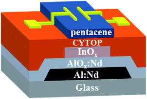 |
| | Fig. 1 Schematic diagram of ambipolar FETs based on InOx/Cytop/pentacene hybrid structure. | |
Results and discussion
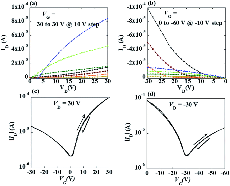
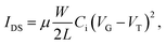
Fig. 2 shows the output and transfer characteristics of the ambipolar FETs based on the organic–inorganic heterostructures with the Cytop layer. The FETs exhibited ambipolar performance with hole and electron mobilities of 1.1 and 0.1 cm2 V−1 s−1, respectively, which were extracted from the following equation,| |
 | (1) |
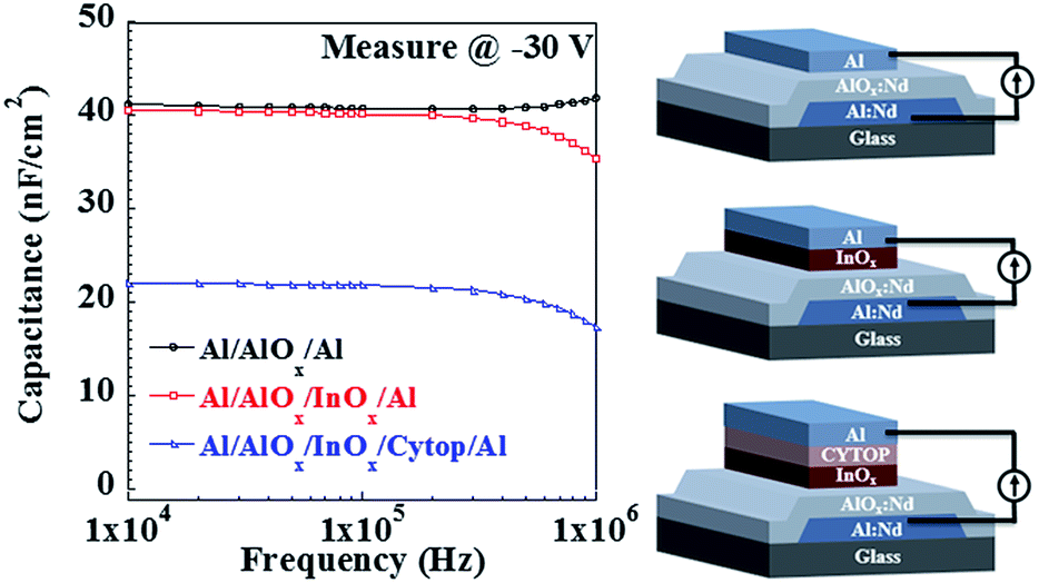
where IDS is drain-source current, VG is gate voltage, VT is the threshold voltage, Ci is capacitance density. Specifically, Ci (22 nF cm−2) for hole mobility and Ci (41 nF cm−2) for electron mobility were different, because the 20 nm thick InOx and 45 nm thick Cytop layer were acted as the dielectric layers when the FET was operated in the p-channel mode, as shown in Fig. 3. Ci for hole mobility was constant as gate voltage varies from 0 V to −30 V, as shown in Fig. S3.†
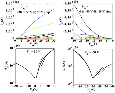 |
| | Fig. 2 Output characteristics of ambipolar FETs based on InOx/Cytop/pentacene hybrid structure: (a) in electron enhancement mode and (b) in electron enhancement mode. Transfer characteristics of ambipolar FETs based on InOx/Cytop/pentacene hybrid structure: (c) VD = 30 V and (d) VD = −30 V. Every curve includes forward and reverse sweeps. | |
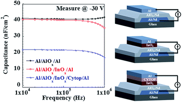 |
| | Fig. 3 Capacitance vs. frequency plots measured at −30 V for AlOx:Nd, AlOx:Nd/InOx and AlOx:Nd/InOx/Cytop; inset: the structures of these three capacitances. | |
It could be also seen from Fig. 2 the hysteresis between the forward and reverse sweeps in the transfer curve is too little to be detected. It implies that the amount of fast traps in the bulk or at the interface is small. It is worth noting that the ambipolar FETs without Cytop or with 20 nm Cytop exhibited large hysteresis, as shown in Fig. S1,† which was attributed to the large amount of hole traps on the surface of InOx (and 20 nm Cytop was not thick enough to block the holes from trapping into InOx). Besides Cytop, polymethyl methacrylate (PMMA) and polystyrene (PS) were also employed as the modification layer. It can be seen from Fig. S2† that the PMMA and PS layer can also improve FET performance, but not as good as Cytop.23,24 Compared to PMMA and PS, Cytop film is smoother and more hydrophobic. Besides, the density of states (DOS) of Cytop film is low due to the low dielectric constant, resulting in higher mobility and better stability.
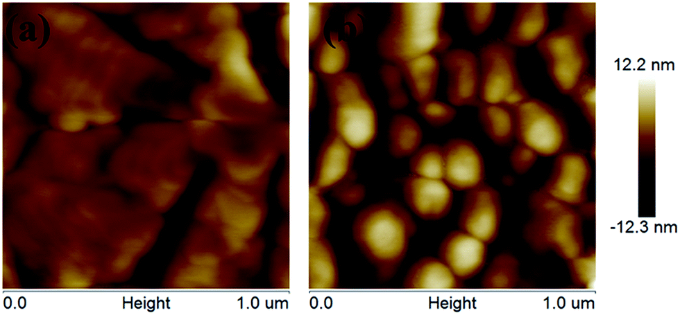
Fig. 4(a) and (b) show the atomic force microscopy (AFM) images of pentacene films on InOx and Cytop/InOx, respectively. The pentacene grain size on InOx was much larger than that on Cytop/InOx. The grain size was based on surface roughness and surface energy. It is known that the pentacene film tends to grow into larger size on the surface of low roughness and high surface energy.25 The roughness of InOx (1.2 nm) is similar as that of Cytop (1.4 nm), tested by AFM. The surface energy of InOx (45.6 mN m−1) is larger than that of Cytop (13.5 mN m−1), which was calculated by OWRK (Owens–Wendt–Rabel–Kaelbe) equation using contact angles of water, ethylene glycol and diiodomethane on the surface of InOx and Cytop.26,27 Although the pentacene grain size on InOx is larger than that on Cytop/InOx, the hole transport of the FETs without Cytop can hardly be detected. This phenomenon was ascribed to the high electron density of InOx. In FETs without Cytop, the large amount of the undepleted electrons can act as the hole traps, so the holes in the organic semiconductor are trapped. After inserted with a Cytop interlayer, the undepleted electrons from InOx are blocked by Cytop, so the holes in pentacene cannot be trapped by the electrons from InOx. As a result, the hole transport of the FETs with Cytop layer improves.
 |
| | Fig. 4 AFM images of pentacene films on (a) InOx, and (b) Cytop/InOx. | |
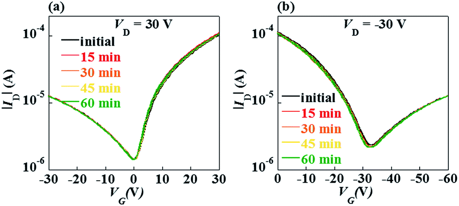
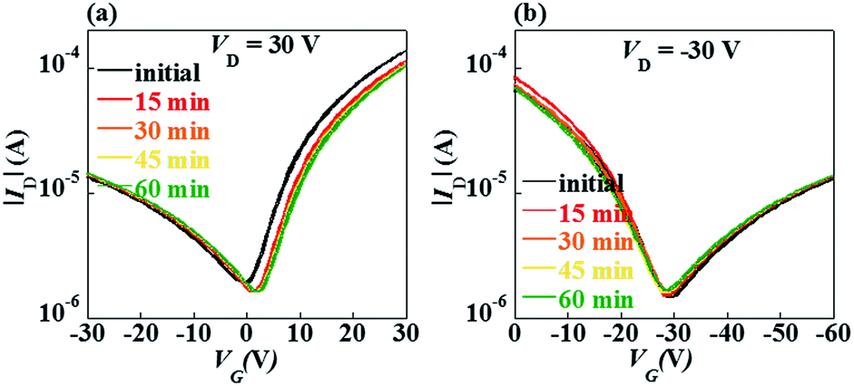
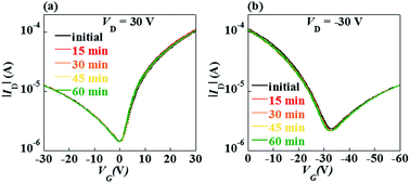
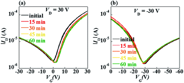
The electrical stability under gate bias stress is an important parameter in FETs. Fig. 5 and 6 show negative bias stress (NBS) and positive bias stress (PBS) stability of the ambipolar FETs, respectively. Almost no threshold voltage shift was found during the PBS test, while a little positive shift was found during the NBS test. The high bias stability was ascribed to the Cytop modification layer. For electron transport, the Cytop acted as the passivation layers to prevent the back channel of InOx from interacting with oxygen and moisture from the air. For hole transport, the Cytop layer can passivated the OH groups on the InOx surface. It is known that the OH groups at the insulator/semiconductor interface would cause device instability. There are no OH groups in the Cytop molecule, and the Cytop films are highly hydrophobic with a water contact angle of 106° which is better than those of many other polymers. Thus, the Cytop modification will improve the electrical stability for both electron and hole transport.22
 |
| | Fig. 5 The time-dependent transfer property ((a) VD = 30 V and (b) VD = −30 V) under negative gate-bias-stress for ambipolar FETs stress condition: VG = 30 V, VD = 30 V. Every curve includes forward and reverse sweeps. | |
 |
| | Fig. 6 The time-dependent transfer property ((a) VD = 30 V and (b) VD = −30 V) under negative gate-bias-stress for ambipolar FETs stress condition: VG = −30 V, VD = −30 V. Every curve includes forward and reverse sweeps. | |
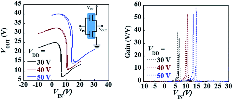
Finally, a complementary-like inverter was fabricated with the integration of two identical pentacene/Cytop/InOx ambipolar FETs. Fig. 7(a) shows the voltage transfer characteristics. The input voltage was applied through the Al:Nd bottom gate electron. Three supply voltages (VDD) of 30 V, 40 V and 50 V were biased to the inverter respectively. The output voltage (VOUT) varied from high to low in response to the swing of the VIN from low to high, and sharp inversions were found to be near 5 V, 10 V and 15 V, respectively. The voltage grain, defined as |dVOUT/dVIN| was calculated from the voltage transfer curves, as shown in Fig. 7(b). The voltage gains reached maximum value of 40, 54 and 58. The VOUT was not constant at both high and low values of VIN, where VOUT increased slightly with VIN. This common feature of ambipolar inverters arose because one of the ambipolar FETs is not completely turned off while the second FET was turned on.15 Overall, the inverter exhibited better electrical stability and voltage gain compared to most of other inverters based on unipolar p-type and n-type FETs and ambipolar FETs.28–30
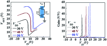 |
| | Fig. 7 (a) The voltage transfer characteristics of the CMOS-like inverter at different supply voltages of 30 V, 40 V, 50 V. Inset: the circuit diagram of the inverter. (b) The corresponding voltage gains of the inverter. | |
Conclusions
In conclusion, the stable ambipolar FETs and CMOS-like inverters based on organic–inorganic heterostructures were fabricated. Pentacene and InOx as the semiconducting p-type and n-type layers composed the hybrid structure. Cytop was inserted to modify the organic–inorganic interface by reducing the surface energy to improve the hole mobility and the stability. As a result the ambipolar FETs showed hole and electron mobilities of 1.1 and 0.1 cm2 V−1 s−1, respectively and excellent electrical stability under gate bias stress. COMS-like inverters showed clear signal inverting operation with a high gain of 58. These results suggest that FETs based on organic–inorganic heterostructures are promising candidates for realizing high stable ambipolar logic devices.
Acknowledgements
This work was supported by the National Key Research and Development Program of China (Grant no. 2016YFB0401105), the National “973” Project of China (Grant no. 2015CB655000), the National Natural Science Foundation of China (Grant no. 51673068, 61204087, and 51173049), the Pearl River S&T Nova Program of Guangzhou (Grant no. 2014J2200053), the Guangdong Province Science and Technology Plan (Grant no. 2013B010403004, 2014B010105008, 2014B090916002, and 2015B090914003).
Notes and references
- A. Dodabalapur, H. E. Katz, L. Torsi and R. C. Haddon, Science, 1995, 269, 1560 CAS.
- J. Zaumseil and H. Sirringhaus, Appl. Phys. Lett., 2007, 107, 1296 CAS.
- B. B. Y. Hsu, E. B. Namdas, J. D. Yuen, S. Cho, I. D. W. Samuel and A. J. Heeger, Adv. Mater., 2010, 24, 4649 CrossRef PubMed.
- Y. Zhao, Y. Guo and Y. Liu, Adv. Mater., 2013, 25, 5372 CrossRef CAS PubMed.
- S. Watanabe, T. Fujita, J. Ribierre, K. Takaishi, T. Muto, C. Adachi, M. Uchiyama, T. Aoyama and M. Matsumoto, ACS Appl. Mater. Interfaces, 2016, 8, 17574 CAS.
- H. Sirringhaus, Adv. Mater., 2014, 26, 1319 CrossRef CAS PubMed.
- B. Kumar, B. K. Kaushik and Y. S. Negi, Polym. Rev., 2014, 54, 3 Search PubMed.
- E. Fortunato, P. Barquinha and R. Martins, Adv. Mater., 2012, 24, 2945 CrossRef CAS PubMed.
- Y. Zhao, Y. Guo and Y. Liu, Adv. Mater., 2013, 25, 5372 CrossRef CAS PubMed.
- K. Nomura, T. Kamiya, H. Ohta, T. Uruga, M. Hirano and H. Hosono, Phys. Rev. B: Condens. Matter Mater. Phys., 2007, 75, 035212 CrossRef.
- L. Lan, N. Xiong, P. Xiao, M. Li, H. Xu, R. Yao, S. Wen and J. Peng, Appl. Phys. Lett., 2013, 102, 242102 CrossRef.
- H. Nakanotani, M. Yahiro, C. Adachi and K. Yano, Appl. Phys. Lett., 2007, 90, 262104 CrossRef.
- J. Smith, A. Bashir, G. Adamopoulos, J. E. Anthony, D. D. C. Bradley, R. Hamiltion, M. Heeney, I. McCulloch and T. D. Anthopoulos, Adv. Mater., 2010, 22, 3598 CrossRef CAS PubMed.
- C. Yang, Y. Kwack, S. H. Kim, T. K. An, K. Hong, S. Nam, M. Park, W. Choi and C. E. Park, Org. Electron., 2011, 12, 411 CrossRef CAS.
- B. Kim, S. Jang, M. L. Geier, P. L. Prabhumirashi, M. C. Hersam and A. Dodabalapur, Appl. Phys. Lett., 2014, 104, 62101 CrossRef.
- J. Shi, H. Wang, D. Song, H. Tian, Y. Geng and D. Yan, Adv. Funct. Mater., 2007, 17, 397 CrossRef CAS.
- E. J. Meijer, D. M. Deleeuw, S. Setayesh, E. V. Veenendaal, B. H. Huisman, P. W. Blom, J. C. Hummelen, U. Scherf and T. M. Klapwijk, Nat. Mater., 2003, 2, 678 CrossRef CAS PubMed.
- K. Baeg, D. Khim, S. Jung, M. Kang, I. You, D. Kim, A. Facchetti and Y. Noh, Adv. Mater., 2012, 24, 5433 CrossRef CAS PubMed.
- I. Meager, M. Nikolka, B. C. Schroeder, C. B. Nielsen, M. Planells, H. Bronstein, J. W. Rumer, D. I. James, R. S. Ashraf, A. Sadhanala, P. Hayoz, J. Flores, H. Sirringhaus and I. McCulloch, Adv. Funct. Mater., 2014, 24, 7109 CAS.
- J. Y. Choi, W. Kang, B. Kang, W. Cha, S. K. Son, Y. Yoon, H. Kim, Y. Kang, M. J. Ko, H. J. Son, K. Cho, H. J. Cho and B. Kim, ACS Appl. Mater. Interfaces, 2015, 7, 6002 CAS.
- Y. Li, L. Lan, P. Xiao, Z. Lin, S. Sun, W. Song, E. Song, P. Gao, P. Zhang and J. Peng, J. Mater. Chem. C, 2016, 4, 2072 RSC.
- S. Sun, L. Lan, P. Xiao, Z. Lin, H. Xu, M. Xu and J. Peng, RSC Adv., 2015, 5, 15695 RSC.
- J. Veres, S. Ogier and G. Lloyd, Chem. Mater., 2004, 16, 4543 CrossRef CAS.
- X. Cheng, M. Caironi, Y. Y. Noh, J. Wang, C. Newman, H. Yan, A. Facchetti and H. Sirringhaus, Chem. Mater., 2010, 22, 1559 CrossRef CAS.
- J. Veres, S. D. Ogier, S. W. Leeming, D. C. Cupertino and S. MohialdinKhaffaf, Adv. Funct. Mater., 2003, 13, 199 CrossRef CAS.
- D. K. Owens and R. C. Wendt, J. Appl. Polym. Sci., 1969, 13, 1741 CrossRef CAS.
- F. M. Fowkes, J. Phys. Chem., 1963, 67, 2538 CrossRef CAS.
- B. Singh, P. Senkarabacak, N. S. Sariciftci, A. Tanda, C. Lackner, R. Hagelauer and G. Horowitz, Appl. Phys. Lett., 2006, 89, 033512 CrossRef.
- M. J. An, H. S. Seo, Y. Zhang, J. D. Oh and J. H. Choi, Appl. Phys. Lett., 2010, 97, 023506 CrossRef.
- J. D. Oh, J. W. Kim, D. K. Kim and J. H. Choi, Org. Electron., 2016, 30, 131 CrossRef CAS.
Footnote |
| † Electronic supplementary information (ESI) available. See DOI: 10.1039/c6ra26817j |
|
| This journal is © The Royal Society of Chemistry 2017 |
Click here to see how this site uses Cookies. View our privacy policy here. 
 Open Access Article
 This Open Access Article is licensed under a Creative Commons Attribution-Non Commercial 3.0 Unported Licence
 *,
Yuzhi Li,
Honglong Ning,
Rihui Yao,
Lei Wang and
Junbiao Peng
*,
Yuzhi Li,
Honglong Ning,
Rihui Yao,
Lei Wang and
Junbiao Peng