
 Open Access Article
 This Open Access Article is licensed under a Creative Commons Attribution-Non Commercial 3.0 Unported Licence
High sensitivity, fast response and low operating voltage organic photodetectors by incorporating a water/alcohol soluble conjugated polymer anode buffer layer
Tiening Wang,
Yufeng Hu *,
Zhenbo Deng*,
Yue Wang,
Longfeng Lv,
Lijie Zhu,
Zhidong Lou,
Yanbing Hou and
Feng Teng
*,
Zhenbo Deng*,
Yue Wang,
Longfeng Lv,
Lijie Zhu,
Zhidong Lou,
Yanbing Hou and
Feng Teng
Key Laboratory of Luminescence and Optical Information, Ministry of Education, Beijing JiaoTong University, Beijing 100044, China. E-mail: yfhu@bjtu.edu.cn; zbdeng@bjtu.edu.cn
First published on 5th January 2017
Abstract
Low dark current density plays a key role in determining the overall performance of organic photodetectors (OPDs). However, both the donor domains and acceptor domains in the bulk heterojunction, which has high exciton dissociation efficiency, are in contact with the two electrodes. Therefore, the undesirable charge injection from the electrodes to the active layer is hard to avoid, leading to a high dark current density in most OPDs. In this work, we fabricate the OPDs based on a conventional poly(3-hexylthiophene) (P3HT)/(phenyl-C61-butyric-acid-methyl-ester) (PC61BM) bulk heterojunction. By incorporating a water/alcohol soluble conjugated polymer (WSCP), poly[(9,9-bis(3′-(N,N-dimethylamino)propyl)-2,7-fluorene)-alt-2,7-(9,9-dioctylfluorene)] (PFN), interlayer between the anode and the active layer, the dark current density is effectively reduced from 0.07 mA cm−2 to 1.92 × 10⁻⁵ mA cm−2 under a −0.5 V bias. The resulting OPDs show a 1.93 × 10⁵ signal-to-noise ratio (SNR), a 10 MHz bandwidth, and a 9.10 × 10¹² Jones detectivity at a low reverse bias of −0.5 V (at 550 nm). Our research provides a promising way for high performance OPDs.
Introduction
Organic photodetectors (OPDs) have been a major focus of basic research due to their potential applications and the intrinsic properties of low cost, light weight, good flexibility, and being printable on plastic substrates compared to their traditional inorganic counterparts.1–3 Along with the rapid development of polymer electronics, the OPDs have attracted more attention because of high sensitivity, fast response speed, and wide spectral response range.4–7 A simple and effective strategy is to blend donor and acceptor materials to form a bulk heterojunction structure based OPD. In the bulk heterojunction, excitons can be efficiently separated into free charge carriers due to the increasing interfaces between donors and acceptors compared with the planar construction.8,9 However, since the active layer is in contact with both the electrodes, holes and electrons can be injected from either a low work function cathode or a high work function anode, which will lead to an undesirable high dark current density and thus significantly degrade the device performance.10 It has been demonstrated that OPDs with an interfacial layer can obtain good performance by decreasing the dark current density of the bulk heterojunction structure. Melancon et al. realized the substantial broadband photoconductive gain in P3HT:PC61BM photodetector by using a semicontinuous Au blocking layer.11 Hammond et al. demonstrated the strong photocurrent gain in OPDs by using naphthalenetetracarboxylic dianhydride (NTCDA) and fullerene (C60) as the dual charge blocking layers.12 Nevertheless, the thermal fabrication of interlayer is a great challenge for all-solution manufacturing. Titanium oxide (TiOx) and zinc oxide (ZnO) are widely investigated as interfacial layer for organic optoelectronic devices owing to their solution-processed preparation and favorable electronic properties, however, the undesired high temperature annealing and other additional processes to achieve better performance limit their applications.13–16 There is a strong need for the development of good performance OPDs with easy and low-cost solution preparation.Due to good processability from water or other polar solvents, water/alcohol soluble conjugated polymers (WSCPs) can be directly used as electrode buffer layer.17 Among all the polyfluorene-based WSCPs, PFN have attracted special attention in organic electronic devices.18–21 J. Miao et al. recently used PFN as the anode buffer layer to demonstrate efficient OPDs based on P3HT and non-fullerene, with a 100![[thin space (1/6-em)]](https://www.rsc.org/images/entities/char_2009.gif) :1 doping-weight ratio.22 The key of their work is the low concentration of the acceptor, which can act as the charge traps and is attributed to the enhanced charge tunneling injection from the external circuit. However, PFN has not been studied in the OPDs based on the common polymer donor P3HT and the fullerene derivative acceptor PC61BM. We first demonstrated the bulk heterojunction OPDs with the structure of ITO/PFN/P3HT:PC61BM/Al. The dark current density of the device can be effectively reduced to 1.92 × 10⁻⁵ mA cm−2 and the OPDs exhibit a 1.93 × 10⁵ signal-to-noise ratio (SNR), a bandwidth of 10 MHz and a detectivity of 9.10 × 10¹² Jones at a low reverse bias of −0.5 V (at 550 nm).
:1 doping-weight ratio.22 The key of their work is the low concentration of the acceptor, which can act as the charge traps and is attributed to the enhanced charge tunneling injection from the external circuit. However, PFN has not been studied in the OPDs based on the common polymer donor P3HT and the fullerene derivative acceptor PC61BM. We first demonstrated the bulk heterojunction OPDs with the structure of ITO/PFN/P3HT:PC61BM/Al. The dark current density of the device can be effectively reduced to 1.92 × 10⁻⁵ mA cm−2 and the OPDs exhibit a 1.93 × 10⁵ signal-to-noise ratio (SNR), a bandwidth of 10 MHz and a detectivity of 9.10 × 10¹² Jones at a low reverse bias of −0.5 V (at 550 nm).
Experimental
Materials
P3HT (Mw = 68000 g mol−1) was purchased from Rieke Metals. PC61BM was purchased from Nano-C. PFN was purchased from 1-Material Inc. All chemicals were used as received without further treatment.
Device fabrication
The OPDs were fabricated with the structure of ITO/PFN/P3HT:PC61BM/Al. The devices without PFN interlayer were also prepared for a comparison. Pre-patterned ITO-coated glass with a sheet resistance of 15 Ω sq−1 was used as the substrate and the anode electrode. The substrate was sequentially cleaned with detergent, de-ionised water, absolute ethanol, acetone, and isopropanol using an ultrasonic bath, followed by UV-ozone treatment for 15 min. The PFN was dissolved in methanol in the presence of a small amount of acetic acid and its solution (concentration, 2 mg ml−1) was spin-coated on top of the pre-cleaned ITO substrate. The thickness of PFN layer is about 10 nm.20 Subsequently, the active layer was prepared by spin-coating the 1,2-dichlorobenzene solution of P3HT and PC61BM (1:1 w/w) and then was annealed at 110 °C for 10 min. Finally, about 100 nm of Al was thermally deposited on the active layer under a vacuum of ∼2 × 10⁻⁴ Pa. The active area of OPDs was 4.5 mm2 (3 mm × 1.5 mm). Fig. 1(a) showed the device structure of OPDs and the molecular structure of PFN. Fig. 1(b) gave the schematic energy levels of OPDs, in which the formation of an interface dipole moment was taken into account.20
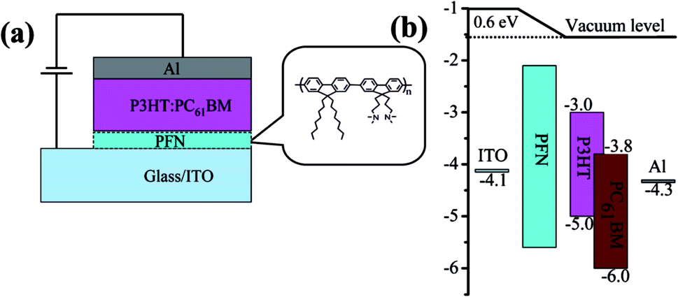 | ||
| Fig. 1 (a) Device structure of the OPDs and the molecular structure of PFN. (b) Schematic energy levels of the OPDs with PFN anode buffer layer, noting that the formation of an interface dipole is also presented. | ||
Device characterization
The current density–voltage (J–V) characteristics were measured by using a Keithley 6430 source-power unit and an Air Mass 1.5 Global (AM 1.5 G) solar simulator with an irradiation intensity of 100 mW cm−2 (SAN-EI Electric XEC-301S solar simulator). Ultraviolet photoelectron spectroscopy (UPS) was recorded by a Kratos Axis Ultra DLD spectrometer using He(I) ultraviolet light (21.22 eV) as the excitation source. Transient photocurrent was investigated by a Tektronix MSO5104B Mixed Signal Oscilloscope with an input impedance of 50 Ω, and a square-pulsed optical excitation of 2 ms was generated from a green-LED (530 nm, 2.94 mW cm−2) driven by a function generator. The capacitance–voltage (C–V) measurements were conducted using an Agilent E4990A impedance analyzer with an AC bias of 25 mV and a frequency of 3 kHz. External quantum efficiency (EQE) spectra were conducted by a Zolix Solar Cell Scan 100. The modulated excitation light at various frequencies was obtained by a WF 1946B multifunction synthesizer (NF Corporation), and the bandwidth was calculated by fast Fourier transform (FFT) algorithm.Results and discussion
Fig. 2 shows the J–V characteristics of the OPDs with and without the PFN anode buffer layer in the dark and under illumination. In the dark, the device with pristine ITO has a current density of 0.07 mA cm−2 at −0.5 V and 0.71 mA cm−2 at −2 V, while the device with the PFN interlayer shows a low current density of 1.92 × 10⁻⁵ mA cm−2 at −0.5 V and 5.84 × 10⁻⁵ mA cm−2 at −2 V. The dark current density of the device with the PFN interlayer is much lower than that of the device with pristine ITO under reverse bias. Besides, the dark current density of the device with PFN interlayer is lower under reverse bias than that under forward bias. The photocurrent density of the device with pristine ITO ranges from 6.04 mA cm−2 at −0.5 V up to 7.54 mA cm−2 at −2 V, compared with those from 3.70 mA cm−2 at −0.5 V up to 8.32 mA cm−2 at −2 V for the device with the PFN interlayer. The devices with the PFN interlayer show an Ion/Ioff (signal-to-noise ratio) of 1.93 × 10⁵ at −0.5 V, which is much higher than that (86.29 at −0.5 V) of the devices without the PFN interlayer. The low dark current density and high Ion/Ioff are attributed to the insertion of the PFN interlayer and the dominant mechanism is discussed below.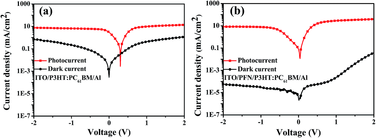 | ||
| Fig. 2 J–V curves of the OPDs with (a) pristine ITO and (b) ITO with PFN anode buffer layer, respectively. | ||
First, the work function of the pristine ITO and ITO/PFN were measured by UPS. In Fig. 3(a), it can be seen that the binding energy is about 16.7 eV for the pristine ITO and 17.3 eV for the ITO with the PFN interlayer, respectively. By subtracting the excitation energy (He Iα source with 21.22 eV), the work function of ITO with PFN interlayer is calculated to be approximately 0.6 eV lower than that of pristine ITO. The formation of an interface dipole is proved to be the major cause for the reduced work function and our result is consistent with previous report.20 Schematic energy level diagram of the OPDs with PFN interlayer is shown in Fig. 1(b). In the dark, the PFN dipole layer can block the electron injection from ITO into the lowest unoccupied molecular orbital (LUMO) of PC61BM under reverse bias, and the hole injection from the Al electrode into the highest occupied molecular orbital (HOMO) of P3HT need to overcome an energy barrier of 0.7 eV. Thus the charge injection from the external circuit is effectively limited, which is beneficial to obtain a low dark current. With light illumination, the photogenerated excitons dissociate at the P3HT-PC61BM interface, generating holes on the P3HT HOMO level and electrons on the PC61BM LUMO level. The photogenerated carriers accumulate around the interface of the PFN dipole layer and the active layer under a reverse bias, which creates an interfacial band bending of 0.6 eV. Therefore, efficient electric charge tunneling through the PFN dipole layer occurs with the help of the accumulated electric charges, leading to a little bit higher photocurrent comparing with the device without PFN layer.23,24
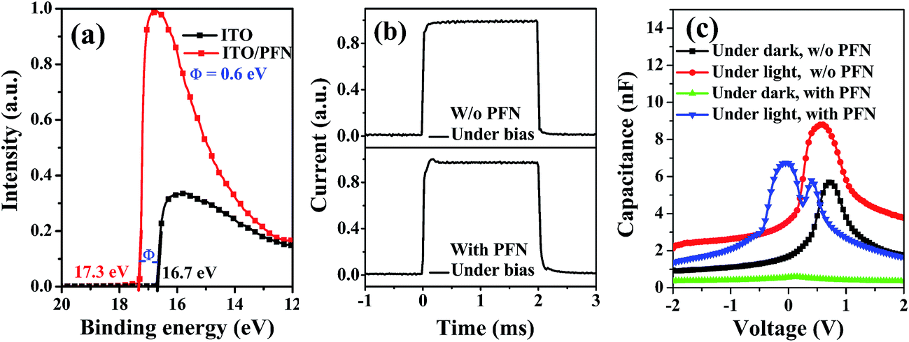 | ||
| Fig. 3 (a) UPS of the pristine ITO and ITO/PFN. (b) Transient photocurrent of the OPDs with and without PFN anode buffer layer at a reverse bias of −0.5 V. (c) C–V characteristics of the OPDs with and without the PFN anode buffer layer under the dark and light conditions. | ||
Transient photocurrent measurement was conducted to interpret the working mechanism of the OPDs with the PFN anode buffer layer. Fig. 3(b) shows the transient photocurrent response of the OPDs with and without PFN interlayer at a reverse bias of −0.5 V. It is obvious that the transient photocurrent of the OPDs with pristine ITO shows a fast turn-on and turn-off dynamics. This fast rise/fall process is a commonly observed feature in P3HT:PC61BM material system, which is usually related to a charge density dependence of mobility.25,26 However, the transient photocurrent of OPDs with the PFN interlayer rises slowly to reach steady state with a smooth overshoot and then experiences a long current decay dynamics compared with that of the control device. This kind of overshoot and the long tail can appear in the organic photoelectric devices with charge carriers trapped in the bulk heterojunction or the interfacial barrier.25,27 The above phenomena of the OPDs with the PFN interlayer can be explained as follows: upon switching on the light, excitons formed in the active layer and they separated at the donor (D)/acceptor (A) interface. Holes drift and diffuse away from the D/A interface to the active layer/PFN interface under reverse bias, where they pile up because of the PFN dipole layer. The hole accumulation close to the PFN interlayer creates an interfacial band bending which can lead to a tunneling electron injection.23,24 If the electric field is not sufficient to completely extract the photocurrent, an overshoot can be seen. When switching off the light, the accumulated charges will release, which leads to a persistent photocurrent tail.27
The C–V measurements were carried out in the dark and under white LED illumination (22.4 mW cm−2) and the results are shown in Fig. 3(c). From dark to illumination, the capacitance of the OPDs with pristine ITO increase from 1.69 nF to 3.61 nF at zero bias, while it increases from 0.57 nF to 6.71 nF for the OPDs with the PFN interlayer. The capacitance increments are 1.92 nF and 6.14 nF for the OPDs without and with PFN interlayer, respectively, which indicates that the OPDs with the PFN interlayer can accumulate much more photogenerated carriers. From −2 V to 2 V, the capacitances of the pristine ITO devices increase up to the peak and then decrease no matter in the dark or under illumination. The voltage with the peak capacitance is defined as the peak voltage (Vpeak), which is usually correlated with the built-in voltage (Vbi).28 For the OPDs with the PFN interlayer, there are two peaks (one is in the negative region and the other one is in the positive region) appeared in the C–V curve under illumination, which indicates that these devices are able to achieve a two-way injection. Under reverse bias, the photogenerated holes will accumulate close to the PFN interlayer and then create an interfacial band bending leading to a tunneling electron injection, which contributes to the peak in the negative region.24,29,30 Under forward bias, both the holes and electrons can inject from the two electrodes, the OPDs show a type Schottky diode behavior of P3HT:PC61BM bulk heterojunction. The capacitance is determined by the depletion layer modulation (V < Vbi) and the storage of minority carriers (V > Vbi).31,32 The low capacitance of the OPDs with PFN interlayer under dark from −2 V to 2 V once again confirms the large injection barrier.
Fig. 4(a) shows the frequency response of the OPDs at a reverse bias of −0.5 V under green-LED illumination (530 nm, 5.55 mW cm−2) and the results have been normalized to the value measured at 50 Hz. The bandwidth reflects the device response to time-modulated incident light, which is crucial for the imaging application.33 Commonly, the bandwidth (−3 dB cut-off frequency) is defined as the frequency at which the photocurrent pulse height is attenuated by a factor of  and it is determined by the transit time of photon-generated carriers traveling from the active layer to the electrodes.34 The −3 dB cut-off frequency of the OPDs with PFN interlayer reaches about 10 MHz, which indicates the fast response.
 | ||
| Fig. 4 (a) Frequency response of the OPDs with PFN anode buffer layer under green-LED illumination (530 nm, 5.55 mW cm−2). (b) EQE spectra and (c) detectivity curve of the OPDs with PFN anode buffer layer at a reverse bias of −0.5 V. | ||
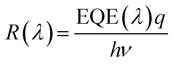
In addition to bandwidth, responsivity (R) and detectivity (D*) are also used to evaluate the performance of OPDs. Especially for D*, it can be calculated from the noise density spectra and the R, and it is the most important physical parameter for a photodetector.35 When operated at reverse bias, the noise is dominated by the shot noise from dark current while the thermal noise contribution can be neglected.35,36 The R and D* can be calculated according to the following equations:7
 | (1) |
 | (2) |
Based on the wavelength coverage of detectivity curve in Fig. 4(c), three kinds of monochromatic light (blue light (468 nm), green light (530 nm) and red light (625 nm)) were selected as the light sources for the I–V measurements. In Fig. 5(a)–(c), the photocurrent of OPDs with PFN anode buffer layer increased gradually along with increasing incident light intensity regardless of the wavelengths in the I–V curves. In particular, the photocurrent increased in the same trend, which resulted in a variation of 0.03–0.05 mA at a reverse bias of −0.5 V. These results indicate that the OPDs can properly work under the common visible light illumination.40
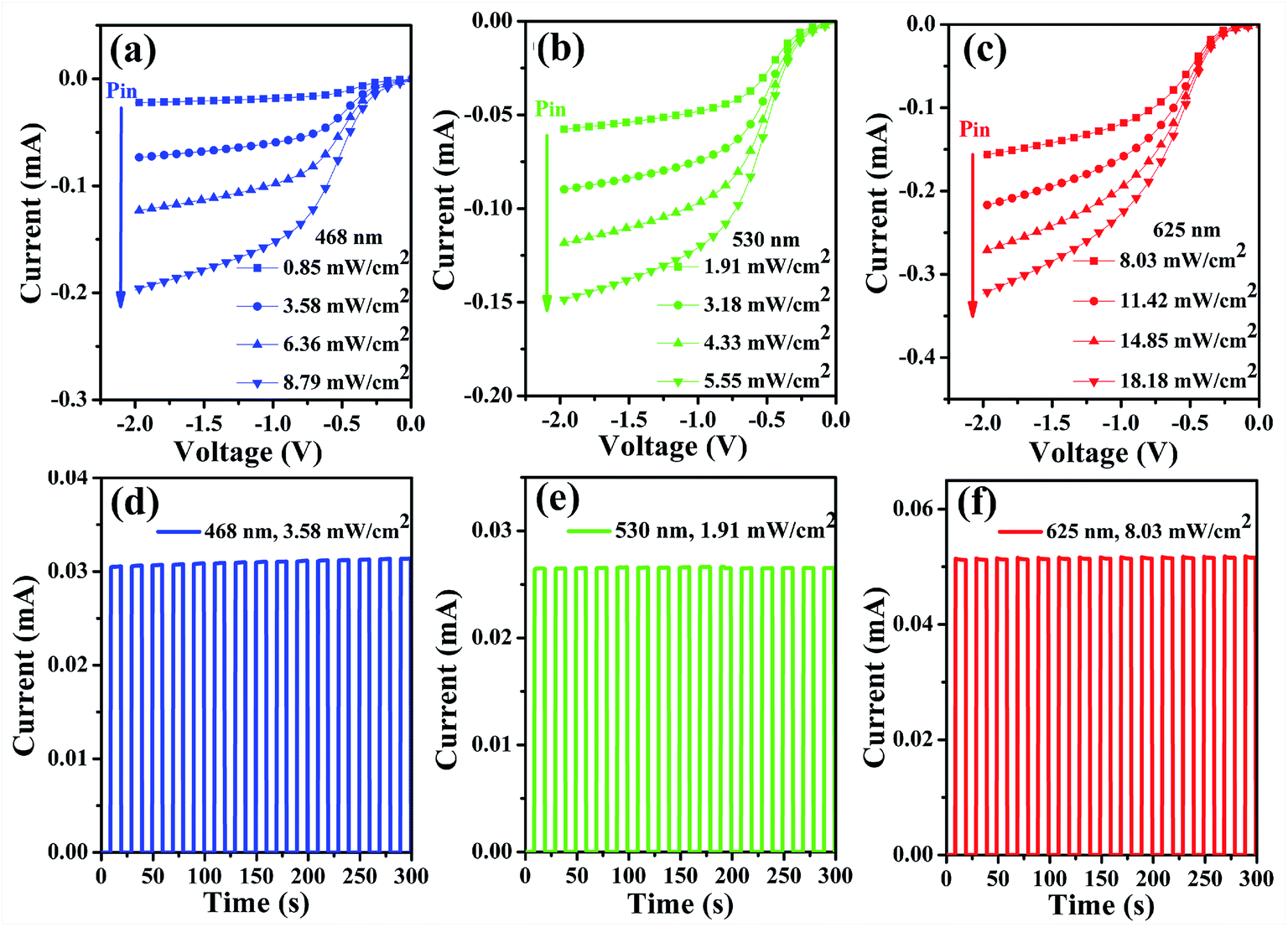 | ||
| Fig. 5 Current–voltage (I–V) characteristics of the OPDs with PFN anode buffer layer under monochromatic illumination of (a) blue light (468 nm), (b) green light (530 nm) and (c) red light (625 nm), and the corresponding incident light intensity (Pin, mW cm−2) from top to bottom in each graph: (a) 0.85, 3.58, 6.36 and 8.79; (b) 1.91, 3.18, 4.33 and 5.55; (c) 8.03, 11.42, 14.85 and 18.18. Photoresponse characteristics of the OPDs with PFN anode buffer layer under on/off modulation of monochromatic light: (d) blue light, 3.58 mW cm−2; (e) green light, 1.91 mW cm−2 and (f) red light, 8.03 mW cm−2, at a reverse bias of −0.5 V. | ||
As shown in Fig. 5(d)–(f), the cyclical photoresponse of OPDs with PFN anode buffer layer was studied by recording the photocurrent signals of the OPDs upon on/off modulation of the monochromatic light (blue light (468 nm, 3.58 mW cm−2), green light (530 nm, 1.91 mW cm−2) and red light (625 nm, 8.03 mW cm−2)) at a reverse bias of −0.5 V. Each cycle is 20 s with an exposure time of 10 s and the total duration is 300 s. The response currents (defined as Ilight − Idark) of the OPDs are about 0.031 mA, 0.026 mA and 0.051 mA respectively, which are almost no obvious changes in the cyclical photoresponse. The little changes of cyclical response currents reveal that the OPDs with PFN interlayer possess stable and reproducible photoresponse.
Conclusions
In conclusion, OPDs based on the P3HT:PC61BM bulk heterojunction structure were fabricated by incorporating the PFN anode buffer layer. The dark current density can be effectively reduced to 1.92 × 10⁻⁵ mA cm−2 and the resulting OPDs exhibit an SNR of 1.93 × 10⁵, a bandwidth of 10 MHz and a detectivity of 9.10 × 10¹² Jones at a low reverse bias of −0.5 V (at 550 nm). The UPS spectra suggest that PFN can lower the work function of ITO due to a dipole interaction, and the transient photocurrent in combination with C–V measurements imply that the OPDs with PFN interlayer experience a large energy barrier. In the dark, the electron injection from the external circuit is effectively limited under reverse bias, which is beneficial to obtain a low dark current. Under illumination, photogenerated carriers form and transport to the electrodes under reverse bias. The holes would pile up close to the PFN and the active layer interface due to the PFN dipole layer and then created an interfacial band bending leading to a tunneling electron injection to the active layer. I–V characteristics and cyclical photoresponses of the OPDs with the PFN interlayer under monochromatic light exhibit the stable and reproducible performance. This work demonstrates the new application of WSCPs as the interlayer in OPDs for achieving better performance.Acknowledgements
The authors acknowledge the financial support of the Fundamental Research Funds for the Central Universities (2014JBZ009) and the National Natural Science Foundation of China (No. 61274063, 61377028, 61475014, 61475017, 61674012, 61675018).Notes and references
- K. J. Baeg, M. Binda, D. Natali, M. Caironi and Y. Y. Noh, Adv. Mater., 2013, 25, 4267–4295 CrossRef CAS PubMed.
- Y. Yao, Y. Liang, V. Shrotriya, S. Xiao, L. Yu and Y. Yang, Adv. Mater., 2007, 19, 3979–3983 CrossRef CAS.
- G. Azzellino, A. Grimoldi, M. Binda, M. Caironi, D. Natali and M. Sampietro, Adv. Mater., 2013, 25, 6829–6833 CrossRef CAS PubMed.
- F.-C. Chen, S.-C. Chien and G.-L. Cious, Appl. Phys. Lett., 2010, 97, 103301 CrossRef.
- L. Shen, Y. Fang, H. Wei, Y. Yuan and J. Huang, Adv. Mater., 2016, 28, 2043–2048 CrossRef CAS PubMed.
- H.-Y. Chen, M. K. F. Lo, G. Yang, H. G. Monbouquette and Y. Yang, Nat. Nanotechnol., 2008, 3, 543–547 CrossRef CAS PubMed.
- X. Gong, M. Tong, Y. Xia, W. Cai, J. S. Moon, Y. Cao, G. Yu, C. L. Shieh, B. Nilsson and A. J. Heeger, Science, 2009, 325, 1665–1667 CrossRef CAS PubMed.
- N. S. Sariciftci, L. Smilowitz, A. J. Heeger and F. Wudl, Science, 1992, 258, 1474–1476 CAS.
- G. Yu, J. Gao, J. C. Hummelen, F. Wudl and A. J. Heeger, Science, 1995, 270, 1789–1791 CAS.
- S. Shafian, Y. Jang and K. Kim, Opt. Express, 2015, 23, A936–A946 CrossRef PubMed.
- J. M. Melancon and S. R. Živanović, Appl. Phys. Lett., 2014, 105, 163301 CrossRef.
- W. T. Hammond, J. P. Mudrick and J. Xue, J. Appl. Phys., 2014, 116, 214501 CrossRef.
- Y. Sun, J. H. Seo, C. J. Takacs, J. Seifter and A. J. Heeger, Adv. Mater., 2011, 23, 1679–1683 CrossRef CAS PubMed.
- X. Zhou, D. Yang, D. Ma, A. Vadim, T. Ahamad and S. M. Alshehri, Adv. Funct. Mater., 2016, 26, 6619–6626 CrossRef CAS.
- S. K. Hau, H.-L. Yip, O. Acton, N. S. Baek, H. Ma and A. K. Y. Jen, J. Mater. Chem., 2008, 18, 5113–5119 RSC.
- H. L. Zhu, W. C. H. Choy, W. E. I. Sha and X. Ren, Adv. Opt. Mater., 2014, 2, 1082–1089 CrossRef CAS.
- Z. He, H. Wu and Y. Cao, Adv. Mater., 2014, 26, 1006–1024 CrossRef CAS PubMed.
- H. W. Fei Huang, D. Wang, W. Yang and Y. Cao, Chem. Mater., 2004, 16, 708–716 CrossRef.
- H. Wu, F. Huang, Y. Mo, W. Yang, D. Wang, J. Peng and Y. Cao, Adv. Mater., 2004, 16, 1826–1830 CrossRef CAS.
- Z. He, C. Zhong, S. Su, M. Xu, H. Wu and Y. Cao, Nat. Photonics, 2012, 6, 593–597 CrossRef CAS.
- Z. He, B. Xiao, F. Liu, H. Wu, Y. Yang, S. Xiao, C. Wang, T. P. Russell and Y. Cao, Nat. Photonics, 2015, 9, 174–179 CrossRef CAS.
- J. Miao, F. Zhang, Y. Lin, W. Wang, M. Gao, L. Li, J. Zhang and X. Zhan, Adv. Opt. Mater., 2016, 4, 1711–1717 CrossRef CAS.
- W. T. Hammond and J. Xue, Appl. Phys. Lett., 2010, 97, 073302 CrossRef.
- K. C. Kao and W. Huang, Electrical transport in solids: with particular reference to organic semiconductors, Pergamon, New York, 1981 Search PubMed.
- Z. Li, F. Gao, N. C. Greenham and C. R. McNeill, Adv. Funct. Mater., 2011, 21, 1419–1431 CrossRef CAS.
- C. G. Shuttle, R. Hamilton, J. Nelson, B. C. O'Regan and J. R. Durrant, Adv. Funct. Mater., 2010, 20, 698–702 CrossRef CAS.
- W. Tress, S. Corvers, K. Leo and M. Riede, Adv. Energy Mater., 2013, 3, 873–880 CrossRef CAS.
- S. L. van Mensfoort and R. Coehoorn, Phys. Rev. Lett., 2008, 100, 086802 CrossRef CAS PubMed.
- S. Lee, J.-H. Lee, K. H. Kim, S.-J. Yoo, T. G. Kim, J. W. Kim and J.-J. Kim, Org. Electron., 2012, 13, 2346–2351 CrossRef CAS.
- S. Lee, J.-H. Lee, J.-H. Lee and J.-J. Kim, Adv. Funct. Mater., 2012, 22, 855–860 CrossRef CAS.
- E. H. Rhoderick and R. H. Williams, Metal–Semiconductor Contacts, Clarendon Press, Oxford, 1988 Search PubMed.
- G. Garcia-Belmonte, A. Munar, E. M. Barea, J. Bisquert, I. Ugarte and R. Pacios, Org. Electron., 2008, 9, 847–851 CrossRef CAS.
- D. Baierl, B. Fabel, P. Gabos, L. Pancheri, P. Lugli and G. Scarpa, Org. Electron., 2010, 11, 1199–1206 CrossRef CAS.
- D. Baierl, B. Fabel, P. Lugli and G. Scarpa, Org. Electron., 2011, 12, 1669–1673 CrossRef CAS.
- S. Wu, B. Xiao, B. Zhao, Z. He, H. Wu and Y. Cao, Small, 2016, 12, 3374–3380 CrossRef CAS PubMed.
- S. M. Sze, Semiconductor Devices: Physics and Technology, John Wiley & Sons Inc, New York, 2001 Search PubMed.
- H. Wei, Y. Fang, Y. Yuan, L. Shen and J. Huang, Adv. Mater., 2015, 27, 4975–4981 CrossRef CAS PubMed.
- L. Li, F. Zhang, W. Wang, Q. An, J. Wang, Q. Sun and M. Zhang, ACS Appl. Mater. Interfaces, 2015, 7, 5890–5897 CAS.
- F. Guo, B. Yang, Y. Yuan, Z. Xiao, Q. Dong, Y. Bi and J. Huang, Nat. Nanotechnol., 2012, 7, 798–802 CrossRef CAS PubMed.
- H. Lee, S. Nam, H. Kwon, S. Lee, J. Kim, W. Lee, C. Lee, J. Jeong, H. Kim, T. J. Shin and Y. Kim, J. Mater. Chem. C, 2015, 3, 1513–1520 RSC.
| This journal is © The Royal Society of Chemistry 2017 |