
 Open Access Article
 This Open Access Article is licensed under a Creative Commons Attribution-Non Commercial 3.0 Unported Licence
Origin(s) of the apparent colossal permittivity in (In1/2Nb1/2)xTi1−xO2: clarification on the strongly induced Maxwell–Wagner polarization relaxation by DC bias
Wattana Tuichaia,
Supamas Danwittayakulb,
Narong Chanlekc,
Pornjuk Srepusharawootad,
Prasit Thongbai*ad and
Santi Maensirie
aDepartment of Physics, Faculty of Science, Khon Kaen University, Khon Kaen 40002, Thailand. E-mail: pthongbai@kku.ac.th
bNational Metal and Materials Technology Center, National Science and Technology Development Agency, 114 Thailand Science Park, Paholyothin Rd, Klong 1, Klong Luang, Pathumthani 12120, Thailand
cSynchrotron Light Research Institute (Public Organization), 111 University Avenue, Muang District, Nakhon Ratchasima 30000, Thailand
dIntegrated Nanotechnology Research Center (INRC), Khon Kaen University, Khon Kaen 40002, Thailand
eSchool of Physics, Institute of Science, Suranaree University of Technology, Nakhon Ratchasima 30000, Thailand
First published on 22nd December 2016
Abstract
The effects of DC bias on the dielectric and electrical properties of co-doped (In1/2Nb1/2)xTi1−xO2 (IN-T), where x = 0.05 and 0.1, and single-doped Ti0.975Nb0.025O2 ceramics are investigated. The low-frequency dielectric permittivity (ε′) and loss tangent of IN-T ceramics with x = 0.05 and 0.1 are greatly enhanced by applying a DC bias at 40 and 20 V, respectively, whereas the relatively high-frequency ε′ remains unchanged. The induced low-frequency Maxwell–Wagner polarization completely vanishes by immediately applying no DC bias. After overload limited measurement, this polarization permanently emerges without DC bias, whereas the primary polarization remains unchanged. Using combined Z′′ and M′′ spectroscopic plots, it is found that the strongly induced-polarizations are contributed from the combination effects of the sample–electrode contact and resistive outer surface. Very high performance of the colossal permittivity in IN-T ceramics is attributed to the formation of a resistive outer-surface layer and insulating grain boundaries. These results not only provide important insights into the origins of the colossal dielectric response in the IN-T ceramic system, but are also important for deciding the doping conditions of TiO2-based materials for practical applications.
1. Introduction
Recently, Hu et al.1 reported a notably high-dielectric performance with an extremely high dielectric permittivity (ε′ ≈ 6 × 10⁴) and an ultra-low dielectric loss tangent (tan![[thin space (1/6-em)]](https://www.rsc.org/images/entities/char_2009.gif) δ ≈ 0.02) over a frequency range of 102 to 106 Hz in (In3+ + Nb5+) co-doped rutile-TiO2 (IN-T) ceramics. By comparing this with previously reported colossal permittivity materials, such as CaCu3Ti4O12 (CCTO),2–4 Ba(Fe1/2Nb1/2)O3,5,6 and co-doped NiO7 ceramics, the temperature stability of IN-T is much better.8 The frequency-independent ε′ of IN-T ceramics was reported to be slightly dependent on temperature over a wide range of 80–450 K.1 Large defect-dipole clusters containing highly localized electrons produced by the complex stoichiometry of (Inx3+Nbx5+Tix3+)Ti1−3x4+O2−x/2 proved to be the origin of these excellent dielectric properties.1
δ ≈ 0.02) over a frequency range of 102 to 106 Hz in (In3+ + Nb5+) co-doped rutile-TiO2 (IN-T) ceramics. By comparing this with previously reported colossal permittivity materials, such as CaCu3Ti4O12 (CCTO),2–4 Ba(Fe1/2Nb1/2)O3,5,6 and co-doped NiO7 ceramics, the temperature stability of IN-T is much better.8 The frequency-independent ε′ of IN-T ceramics was reported to be slightly dependent on temperature over a wide range of 80–450 K.1 Large defect-dipole clusters containing highly localized electrons produced by the complex stoichiometry of (Inx3+Nbx5+Tix3+)Ti1−3x4+O2−x/2 proved to be the origin of these excellent dielectric properties.1
In the pioneering study,1 two primary dielectric relaxations were observed in IN-T ceramics. The primary low-temperature dielectric relaxation (10–50 K), which gives rise to temperature-independent colossal permittivity over a wide range, is due to freezing electrons in defect-dipoles. The other relaxation caused by an extrinsic effect was observed in the range of 450–720 K. Other studies reported that there are at least two additional dielectric relaxations that also occur in the temperature ranges of 50–150 K and 200–300 K; these relaxations are attributed to polaron hopping and interfacial polarization (or space-charge polarization or Maxwell–Wagner polarization), respectively.8–10 Most recently, it was demonstrated that the sample–electrode interface has a remarkable effect on the colossal permittivity of IN-T ceramics and (Ga + Nb) co-doped TiO2 ceramics.10–12 This means that there are several factors that have significant influences on the dielectric properties of TiO2-based materials. Even though the electron-pinned defect-dipole model has been a reasonably novel model for describing the origin of the high-performance dielectric properties of IN-T ceramics, Maxwell–Wagner polarization at the grain boundaries (GB) (i.e., the internal barrier layer capacitor effect, IBLC) has also been proposed as their exact origin,11,13–17 which creates significant confusion. Thus, the origin of the high performance dielectric properties of TiO2-based ceramics must be clarified.
The relaxation phenomenon in a dielectric material is generally undesirable for practical applications due to the resulting large changes in dielectric properties. However, it may give some important clues about the underlying mechanism governing the intriguing dielectric behavior in different temperature and frequency ranges.1,9,18,19 Investigation of dielectric relaxation can elucidate the possible sources of polarization in a particular frequency range.8,9,18
From the point of view of capacitor applications, the DC voltage bias-dependence of ε′ is one of the most important parameters used to justify the use of dielectric materials for low or high-voltage application. From the academic point of view, the effects of DC bias on electrical and colossal dielectric properties may also give some important clues to understanding the overall dielectric responses in these materials, just as the investigation of dielectric relaxation.20–23 Usually, in the case where there are accumulated charges at the sample–electrode contact or where internal interfaces are the primary polarization source, these charges would be stress-induced by applying a DC bias. Eventually, if the applied DC bias is sufficiently high, the accumulated charges could become induced-mobile charges and move across the electrostatic potential barrier at these interfaces, giving rise to DC conductivity (σdc) and correlated low-frequency tanδ values. Concurrently, DC bias also can cause a decrease in the amount of accumulated charges, which leads to a decrease in the intensity of Maxwell–Wagner polarization and ε′.22,23 For CuO and La2−xSrxNiO4 ceramics, in which their colossal dielectric responses are dominated by the non-ohmic sample–electrode effect,22,24 the low-frequency ε′ values at room temperature (RT) can easily be reduced by applying DC bias at 0–4 and 0–1.5 V, respectively. The low-frequency ε′ value (at 200 °C) caused by the sample–electrode effect for a CCTO ceramic was decreased by applying DC bias at 0–2 V.21 For the effect of DC bias on the GB response in CCTO ceramics, variations in their dielectric and electrical properties are dependent on their microstructures (e.g., mean grain size and grain size distribution).20 This had a great effect on the coarse-grained CCTO ceramic (grain size ≈100 μm), but no effect on the small-grained CCTO ceramic (≈5 μm) in the range of 0–15 V DC bias.
Unfortunately, systematic investigation of the effects of DC bias and consequently the resulting dielectric relaxation on the colossal dielectric response and electrical properties of bulk IN-T ceramics have never been reported. Thus, the main objective of this study is to investigate the influence of DC bias to clarify the origin of the colossal dielectric properties of IN-T ceramics and to design materials for practical application. We found that the strong polarization relaxation of IN-T ceramics with high concentrations of co-dopants was easily induced in the low frequency range as a result of the applied DC bias. In contrast, the dielectric properties at 1 kHz of IN-T ceramics with low concentrations of co-dopants was slightly dependent on DC bias in the range of 0–40 V. The high ε′ value in the high frequency range remained unchanged by the application of a DC bias, which indicates the DC bias independence of the primary polarization in IN-T ceramics. The possible sources of polarizations in different frequency ranges are discussed and clarified.
2. Experimental
(In1/2Nb1/2)xTi1−xO2 ceramics with x = 0.05 and 0.1 (abbreviated as 5% IN-T and 10% IN-T, respectively) as well as an Nb-doped TiO2 (Ti0.975Nb0.025O2, 2.5% N-T) ceramic were prepared using a solid state reaction method. TiO2 (>99.9% purity), Nb2O5 (99.99% purity), and In2O3 (99.99% purity) were used as the starting raw materials. Details of the preparation method are given elsewhere.8 The 5% IN-T and 10% IN-T ceramics were obtained by sintering at 1500 °C for 5 h. The sintering conditions for the pure-TiO2 and the Nb-doped TiO2 ceramics were 1400 °C for 5 h.X-ray diffraction (XRD; Bruker, D2 PHASER) was used to characterize the phase composition and crystal structures of all the sintered ceramics. Rietveld quantitative phase analysis was carried out using the X'Pert High Score Plus v3.0e software package by PANalytical. The microstructure and elemental distribution in the IN-T ceramics were examined using field-emission scanning electron microscopy (FE-SEM) with energy-dispersive X-ray analysis (EDX) (HITACHI SU8030, Japan). The chemical states of Ti were analyzed using X-ray photoelectron spectroscopy (XPS, PHI5000 VersaProbe II, ULVAC-PHI, Japan) at the SUT-NANOTEC-SLRI Joint Research Facility, Synchrotron Light Research Institute (SLRI), Thailand. XPS spectra were fitted with the PHI MultiPak XPS software using a combination of Gaussian–Lorentzian lines. Before electrical measurements, Au was sputtered onto each pellet face (not polished) at a current of 25 mA for 8 min using a Polaron SC500 sputter coating unit (Sussex, UK). Dielectric properties were measured under an AC oscillation voltage of 0.5 V using an Agilent 4294A Precision Impedance Analyzer and KEYSIGHT E4990A Impedance Analyzer over the frequency range of 102 to 106 Hz. Dielectric measurements were performed under different DC bias levels.
3. Results and discussion
The XRD patterns of the sintered pure-TiO2, 2.5% N-T, 5% IN-T and 10% IN-T ceramics are given in Fig. 1. All the XRD patterns show the main phase of rutile-TiO2 (JCPDS 21-1276) with a tetragonal structure without an impurity phase. Lattice parameters (a and c) were calculated from Rietveld refinement profile fits. The a and c values of the TiO2, 2.5% N-T, 5% IN-T and 10% IN-T ceramics were found to be 4.592(2) and 2.959(6) Å, 4.595(6) and 2.962(6) Å, 4.599(2) and 2.965(8) Å and 4.601(4) and 2.967(3) Å, respectively. The a and c values of the 10% IN-T ceramic are comparable to the reported values of a ≈ 4.615 Å and c ≈ 2.980 Å in the literature for a 10% (In + Nb) sample.1 Both a and c parameters of the 2.5% N-T, 5% IN-T and 10% IN-T ceramics are larger than those of the sintered pure-TiO2 ceramic and rutile-TiO2 with a = 4.593 Å and c = 2.959 Å (JCPDS 21-1276). It was also observed that both a and c parameters increased with an increase in doping concentration. This enlargement in the lattice parameters is attributed to the larger ionic radii of In3+ and Nb5+ than those of the host Ti4+ ion. This clearly indicates that both In3+ and Nb5+ doping ions entered the rutile-TiO2 lattice structure.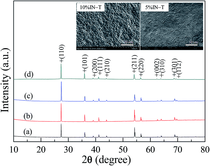 | ||
| Fig. 1 XRD patterns of the (a) pure-TiO2, (b) Nb-doped TiO2, (c) 5% IN-T and (d) 10% IN-T ceramics; inset reveals the surface morphologies of the 5% IN-T and 10% IN-T ceramics. | ||
The insets of Fig. 1 show the microstructure of the 5% IN-T and 10% IN-T ceramics, which reveal GB and grain structures, with mean grain sizes of ≈27.3 ± 5.8 and ≈22.8 ± 4.7 μm, respectively. Residual pores were also observed in the microstructure of the 10% IN-T ceramic, whereas they were not present in the pure-TiO2, Nb-doped TiO2 and 5% IN-T ceramics. To further analyze the distributions of all the elements in the 10% IN-T ceramic, mapping of Ti, O, In, and Nb elements was performed. As shown in Fig. 2, the dopants were homogeneously dispersed in both the grain and GB. No segregation of In3+ and Nb5+ ions at any specific region was observed.
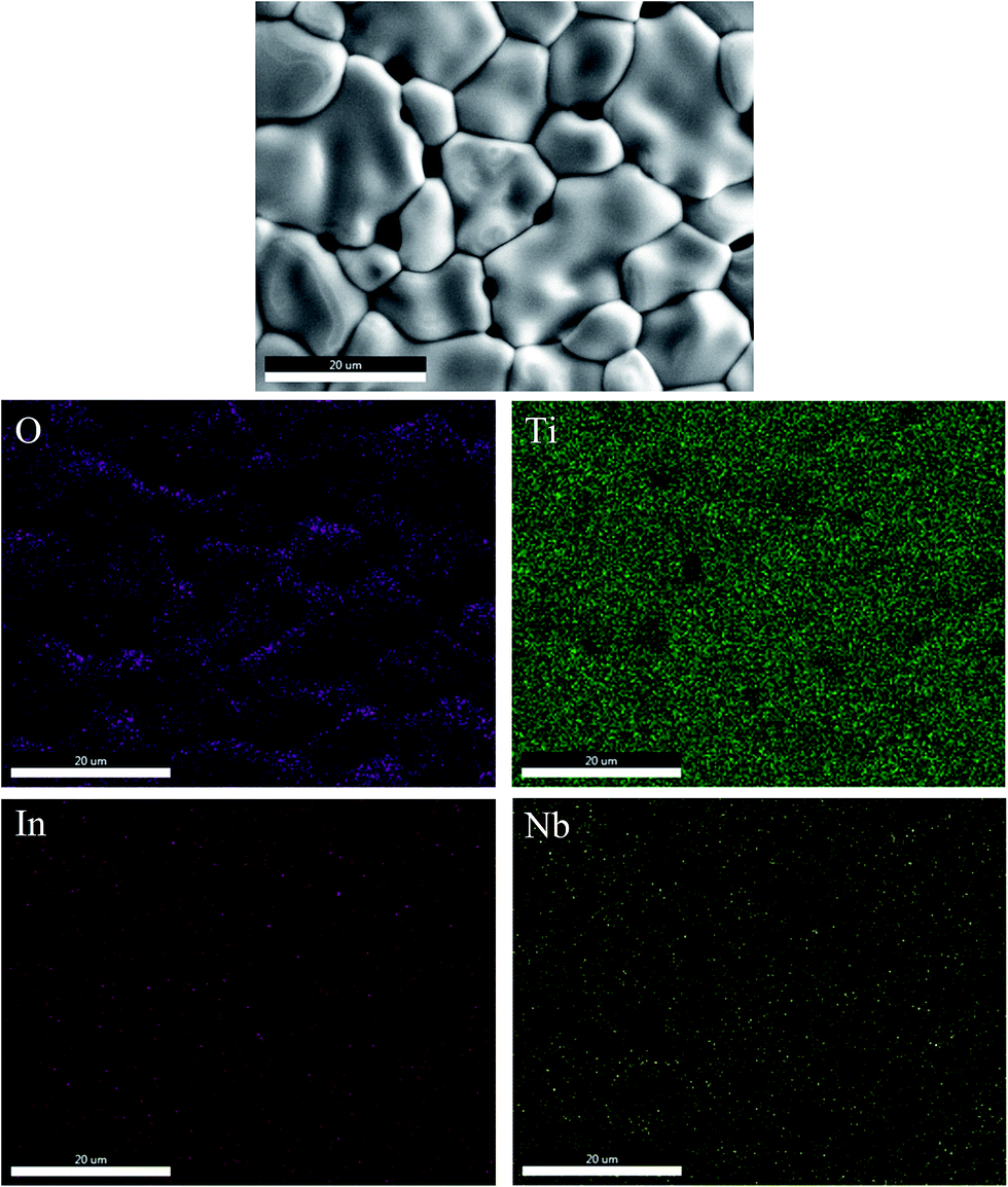 | ||
| Fig. 2 SEM image and element mapping of the 10% IN-T ceramic. | ||
The oxidation states of the polyvalent cations in the 10% IN-T ceramic were identified by XPS spectroscopy, as shown in Fig. 3. Using Gaussian–Lorentzian profile fitting, the XPS spectrum of Ti 2p was found to be consisted of two peaks. The main peak at the binding energy of about ≈458.80 eV can be ascribed to the presence of Ti4+.1,16,17,25 The other peak at a relatively lower binding energy of ≈457.35 eV indicates the existence of Ti3+.1,16,17 The Ti3+/Ti4+ ratio was about 4.29%. Substitution of Nb5+ into TiO2 can produce free electrons by reducing Ti4+ to Ti3+ as follows:
 | (1) |
| Ti4+ + e → Ti3+. | (2) |
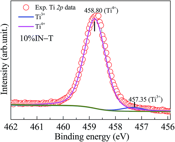 | ||
| Fig. 3 XPS spectrum of the 10% IN-T ceramic for the Ti 2p region. | ||
Very high ε′ of IN-T ceramics should be correlated with the produced free electrons, which can be considered as the sources of polarization at any microscopic region (e.g., GBs, domain boundary, outer surface and sample–electrode interface) and/or at local structures (e.g., detect clusters).
Without an applied DC bias, the 10% IN-T ceramic exhibits excellent dielectric properties with ε′ ≈ 4.9 × 10⁴ and tanδ ≈ 0.052 at 103 Hz and RT, as shown in Fig. 4(a) and its inset, and ε′ is slightly dependent on frequency from 102 to 106 Hz. The values of ε′ and tanδ are comparable to those published in the literature.1 These excellent dielectric properties may have originated from either the electron-pinned defect-dipoles or strong interfacial polarization effect.1,11,13,14 The exact origin will be discussed hereafter.
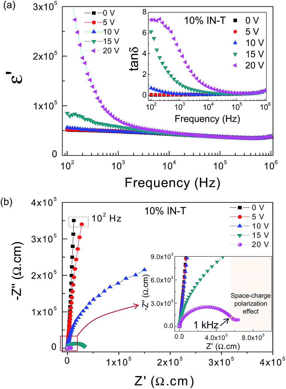 | ||
| Fig. 4 (a) Effect of DC bias (0–20 V) on ε′ at RT for the 10% IN-T ceramic in the frequency range of 102 to 106 Hz and inset demonstrates the influence of DC bias on tanδ. (b) RT–impedance complex plane (Z*) plot as a function of DC bias (0–20 V) for the 10% IN-T ceramic and the inset is an enlarged view of the Z* plot near the origin. | ||
As illustrated in Fig. 4(a), the ε′ of the 10% IN-T ceramic in the frequency range of 102 to 103 Hz increased with an increase in the DC bias from 0 to 20 V using step increments of 5 V per step. When the DC bias was increased to 25 V, an overload limited measurement (OLM) occurred. This is generally due to large current leakage passing through the bulk sample. A drastically increased ε′ was observed in the low frequency range when the DC bias increased from 15 to 20 V. Either hopping of the charge transport of free charges or strong Maxwell–Wagner-polarization (or space charge polarization) relaxation induced by DC bias may have been the primary cause of this observation.26 In the former case, hopping conduction usually leads to typical power-law frequency dependencies of the Universal Dielectric Response (UDR), in which there are characteristic signatures in the frequency dependence of the complex conductivity and permittivity, which follow the relationships σ′ = σ0νs and ε′ ∝ νs−1 (s < 1), respectively.26 In the latter case, a high plateau in the ε′ value in a low-frequency range coupled with a relaxation tanδ peak are usually observed.7,26,27
In the inset of Fig. 4(a), a low-frequency tanδ peak appears when DC bias is 20 V, whereas the plateau of ε′ is not observed. The disappearance of the ε′ plateau may have been due to the fact that the frequency at which there was a step-like decrease in ε′ (or at which the ε′′ – peak appeared) was lower than the frequency of the tanδ peak by a value of 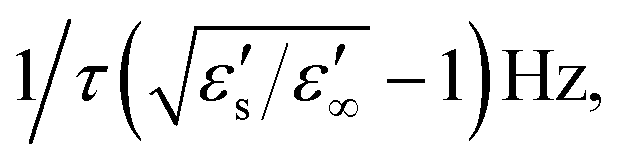 where ε′s and ε′∞ are the ε′ values in the low and high frequency ranges, respectively, and τ is the relaxation time.28 Thus, it is likely that a strong low-frequency Maxwell–Wagner polarization was created by applying a DC bias. It is noteworthy that the ε′ of the 10% IN-T ceramic at frequencies higher than 104 Hz was independent of the DC bias (0–20 V). This indicates that DC bias has no effect on the primary source of the polarization that gives rise to the high-dielectric performance in IN-T ceramics.
To clarify the possible origins of the additional Maxwell–Wagner polarization and the primary polarization, impedance spectroscopy analysis was performed under different DC bias voltages. Without an applied DC bias, only the linear region of an arc with a high-frequency near-zero intercept is observed from the Z* plot at RT in Fig. 4(b), which is similar to that reported by Hu et al.1 They suggested that the complex impedance at RT contains only one constituent intra-grain contribution, which is considered to be the source of the primary polarization. This resistance is roughly estimated to be >100 MΩ cm. This value is consistent with the result reported by Wu et al.,11 in which the resistance estimated from the large semicircle arc of the (Nb0.5In0.5)0.01Ti0.99O2 ceramic was found to be ≈1500 MΩ cm. They suggested that this very high resistance value is attributed to the GB response, at which primary polarization occurs. This is a significant controversy concerning primary polarization, which must be clarified.
The diameter of the semicircle arc dramatically decreased on increasing the applied DC bias. The resistance of the 10% IN-T ceramic was reduced by 3 and 4 orders of magnitude after applying a 15 and 20 V DC bias, respectively [inset of Fig. 4(b)]. At 20 V DC bias, the corresponding resistance was as low as ≈6 × 10³ Ω cm. Furthermore, a low-frequency tail was observed. This may be attributed to the interfacial effect, which is consistent with the variations in ε′ and tanδ values [Fig. 4(a)]. In addition to a large semicircle arc, a nonzero intercept on the Z′ axis was observed, which corresponds to the electrical response of a semiconducting part with the resistance of 15–20 Ω cm (not shown). Thus, the observed large semicircle arc should be due to the electrical response of an insulating part(s) (e.g., another phase, a resistive outer-surface layer, grain boundaries and/or domain boundaries). For a coarse-grained CCTO ceramic (grain size ≈ 100 μm), the GB resistance (Rgb) was greatly reduced by increasing the DC bias from 0 to 15 V. The GB capacitance (Cgb), which is related to the ε′ value, also significantly decreased.20 For a fine-grained CCTO ceramic (grain size ≈ 5 μm), its Rgb value slightly decreased from 4 MΩ (no DC bias) to ≈2.5 MΩ at 4 V and remained constant up to 15 V DC bias. By considering the grain size of ≈22.8 μm for the 10% IN-T ceramic, it is possible that Rgb could be reduced by applying a DC bias of 15–20 V. However, the primary dielectric response in the 10% IN-T ceramic remained unchanged, exactly as reported in the case of the coarse-grained CCTO ceramic.
When the DC bias was increased to 25 V, OLM occurred due to large current leakage. This situation indicates that a large number of induced-mobile charges passed through the bulk ceramic into the circuit. After that, for 24 h, the dielectric properties of the 10% IN-T ceramic were measured again at RT without an applied DC bias (hereafter referred to as the 10% IN-T_A1 sample). In Fig. 5(a), an additional ε′ plateau for the 10% IN-T_A1 sample is observed in the low-frequency range. Concurrently, the step-like decrease in ε′ and corresponding tanδ peak shifted to a high frequency range [Fig. 5(b)]. After a large number of mobile charges produced by applying a DC bias at 25 V, the dominant effect of the induced-Maxwell–Wagner polarization was extended to a higher frequency range. Generally, when the distance between the adjacent barriers in a dielectric is shortened and/or the density of mobile charges in the conductive part is sufficiently large, the frequency range of sensitivity for Maxwell–Wagner polarization (or space-charge polarization) can usually be extended to a higher frequency range. The latter cause is therefore responsible for the observed movement of the induced-Maxwell–Wagner polarization to a higher frequency range. A large semicircle arc in the low-frequency range for an insulating part (in which space-charge polarization was induced) and another electrical response of an insulating part with a smaller semicircle arc are observed [Fig. 5(c)]. The nonzero intercept did not change after the occurrence of OLM, as shown in Fig. 5(d). There are at least three electrical responses in the 10% IN-T ceramic, i.e., (1) grains, (2) GBs and (3) unknown insulating part(s). Among these, at least two insulating parts are contained in the large semicircle arc of the 10% IN-T ceramic. The nonzero intercept and relatively small semicircle arc can be assigned to be electrical responses of the semiconducting grains and GBs, respectively.
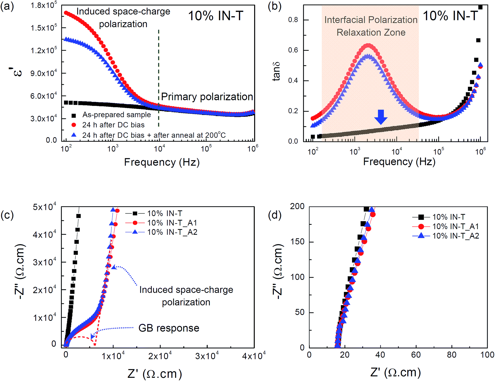 | ||
| Fig. 5 Effects of aging (24 h) and annealing (at 200 °C in air for 0.5 h) for the 10% IN-T ceramic on (a) ε′ and (b) tanδ values at RT in the frequency range of 102 to 106 Hz without DC bias. (c) Z* plots at RT for untreated, aged, and annealed samples measured without DC bias. The dashed red line is a guideline for estimating Rgb. (d) Expanded view of the high-frequency data close to the origin for the Z* plots of (c), revealing the nonzero intercept on the Z′ axis. | ||
The unknown insulating part(s) with a very large resistance compared to Rgb might be caused by trapped-charges at the sample–electrode contact. The ε′ value contributed by the polarization at the sample–electrode contact can be completely eliminated by annealing the sample–electrode contact at 200–300 °C.22,29 To further clarify the possible origin of the large induced-Maxwell–Wagner polarization, the 10% IN-T_A1 sample was annealed in air at 200 °C for 0.5 h (referred to as the 10% IN-T_A2 sample). Annealing had a slight influence on the low-frequency values of ε′ and tanδ [Fig. 5(a) and (b)]. As shown in Fig. 5(c), the large induced-Maxwell–Wagner polarizations of the 10% IN-T_A1 and 10% IN-T_A2 samples were not significantly different. These results clearly indicate that the sample–electrode contact has a slight effect, but it cannot be ignored.
To clearly show the effects of DC bias on the electrical responses of the GBs and non-ohmic sample–electrode contact of TiO2-based ceramics, the dielectric and electrical properties of a single-doped 2.5% N-T ceramic were investigated at RT as a function of DC bias. As shown in Fig. 6(a), two colossal dielectric responses are observed in the frequency range of 102 to 106 Hz. The low-frequency colossal dielectric response (LFCDR) was significantly reduced by DC bias, whereas the relatively high-frequency dielectric response did not change. A nonzero intercept with two semicircle arcs are observed in the Z* plot [Fig. 6(b) and its inset]. At least three electrical responses are confirmed to exist in the 2.5% N-T ceramic. The diameter of the large semicircle arc was remarkably decreased by DC bias, whereas the relatively small semicircle arc and nonzero intercept did not change. These are generally assigned as the electrical responses of the sample–electrode contact, GBs and grains. The effects of DC bias on the electrical response of the sample–electrode contact and associated colossal dielectric properties of the 2.5% N-T ceramic are similar to those observed in other colossal dielectric materials such as CuO, CCTO and La2−xSrxNiO4 ceramics.21,22,24 It is notable that the relaxation frequency of the tanδ peak did not change [inset of Fig. 6(a)]. Only the low-frequency tanδ was greatly increased by the DC bias. These results indicate that the unique characteristic of the sample–electrode effect was easily degraded by the release of trapped charges at the non-ohmic contact during the application of a DC bias.
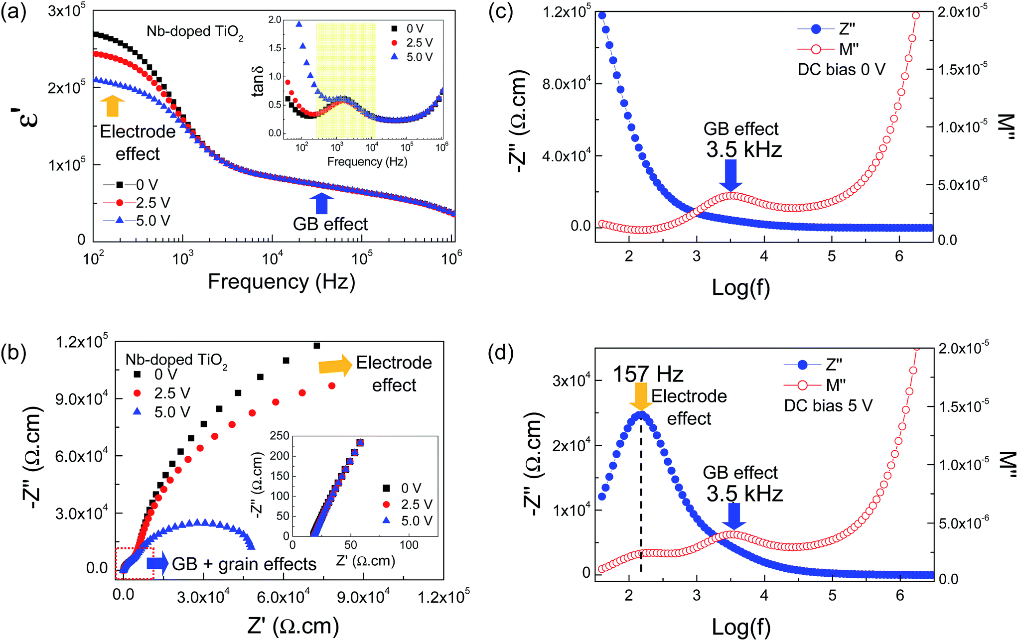 | ||
| Fig. 6 (a) Effect of DC bias (0–5 V) on ε′ at RT for the Nb-doped TiO2 ceramic in the frequency range of 102 to 106 Hz; inset demonstrates the influence of DC bias on tanδ. (b) Z* plot at RT as a function of DC bias (0–5 V) for the Nb-doped TiO2 ceramic; inset is an enlarged view of the Z* plot near the origin, revealing the nonzero intercept due to the grain response. (c and d) Combined Z′′ and M′′ spectroscopic plots at RT for the Nb-doped TiO2 ceramic without and with 5 V DC bias, respectively. | ||
To further confirm each of these electrical responses in the 2.5% N-T ceramic, combined Z′′ and M′′ spectroscopic plots were obtained at RT under 0 and 5 V DC bias, as shown in Fig. 6(c) and (d). Without DC bias, a single M′′ peak is observed at fmax-phase2 ≈ 3.5 kHz. The other M′′ peak shifts above the upper frequency limit (fmax-phase1 > 10 MHz), which indicates that this phase is very conductive, and thus corresponds to the nonzero intercept [inset of Fig. 6(b)]. This phase 1 is reasonably assigned as the semiconducting grain. The fmax-phase3 of the Debye-type peaks in the Z′′ plot occurred below the lower measuring frequency limit of the instrument (<40 Hz). Increasing temperature measurement is usually performed to decrease the resistance value in order to move the fmax-phase3 into the measured frequency range, with regard to the general relationship fmax = 1/2πRC. In this study, the resistance of phase 3 was reduced by applying a DC bias (5 V), thus moving fmax-phase3 in the Z′′ plot as well as in the M′′ plot to the frequency of 157 Hz [Fig. 6(d)]. Phase 3 is presumably correlated to an electrode effect. It is important to note that the M′′ peak height and fmax-phase2 did not change before and after the applied 5 V DC bias, indicating unchanged C and R values, respectively. This phase can be referred to as the insulating GBs.
Now, it is clear to distinguish the LFCDR mechanisms between the 10% IN-T and 2.5% N-T ceramics. The LFCDR in the former case was greatly induced to exist by DC bias; for the latter case, it already appeared and was then destroyed by DC bias. Generally, the non-ohmic sample–electrode contact is created at the interface between the semiconductive ceramic surface and conductive-metal electrode. The existence of semiconducting grains of the 10% IN-T ceramic has been confirmed; however, the effect of the non-ohmic sample–electrode contact was not dominant (LFCDR induced without DC bias). This means that the outer surface region facing the metal-electrode may not be a semiconductor, but an insulator.
At RT, OLM did not occur in the 5% IN-T ceramic even at 40 V DC bias, which indicates very high resistances of its outer-surface layer and/or insulating GBs compared to that of the 10% IN-T ceramic, as shown in Fig. 7(a). Clearly, the LFCDR can also be induced. The induced polarization relaxation, i.e., a step-like decrease in ε′ and corresponding relaxation tanδ peak, shifts to a high frequency as the DC bias increases [Fig. 7(a) and its inset]. The primary dielectric response still did not change, just as observed in the 10% IN-T ceramic. After the dielectric properties of the 5% IN-T ceramic were measured at RT under 40 V DC bias, this sample was immediately measured again without DC bias. It was found that the dielectric properties before and after the applied DC bias at 40 V were nearly the same in value, as illustrated in Fig. 8(a) and its inset. As shown in Fig. 8(b), at 40 V DC bias, the two semicircle arcs of the insulating parts were separated. The Rgb value corresponding to the small semicircle arc at higher frequencies was estimated to be ≈150 kΩ cm. This result implies that if the applied 40 V DC bias also affects the electrical properties of the GBs, without DC bias the RT value of Rgb for the 5% IN-T ceramic should be at least as large as 150 kΩ cm. Note that the impedance spectra under DC bias of the 5% IN-T and 10% IN-T ceramics are very similar. In IN-T ceramics, the inhomogeneous dielectric behavior can be rather pronounced: Rgb and Rg can differ by a factor of up to ≈104. The conduction activation energy associated with either grain or GB conduction processes is expected to differ by up to a factor of >10. Thus, the IBLC can suitably be used to describe the very large ε′ value in IN-T ceramics.
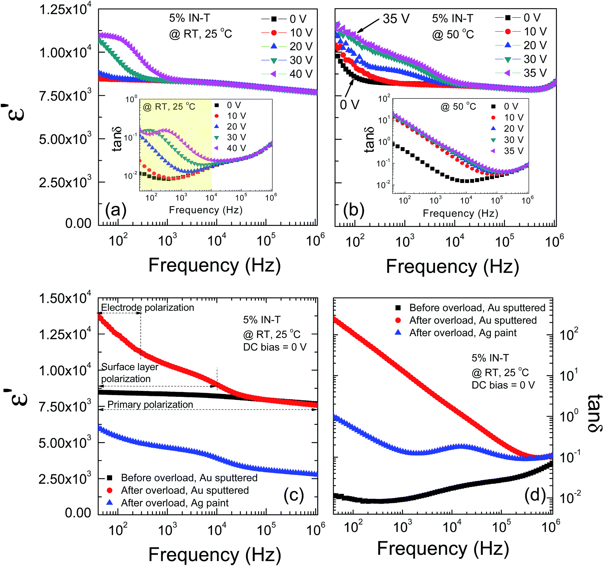 | ||
| Fig. 7 (a and b) Frequency dependence of ε′ under different DC bias voltages for the 5% IN-T ceramic at RT (≈25 °C) and 50 °C, respectively; the insets illustrate the effect of DC bias on tanδ at RT (≈25 °C) and 50 °C. (c and d) ε′ and tanδ at RT without DC bias (0 V) for the as-fired 5% IN-T ceramic sample and 5% IN-T ceramic samples after an overload limited DC bias measurement using Au-sputtered and Ag paint electrodes. | ||
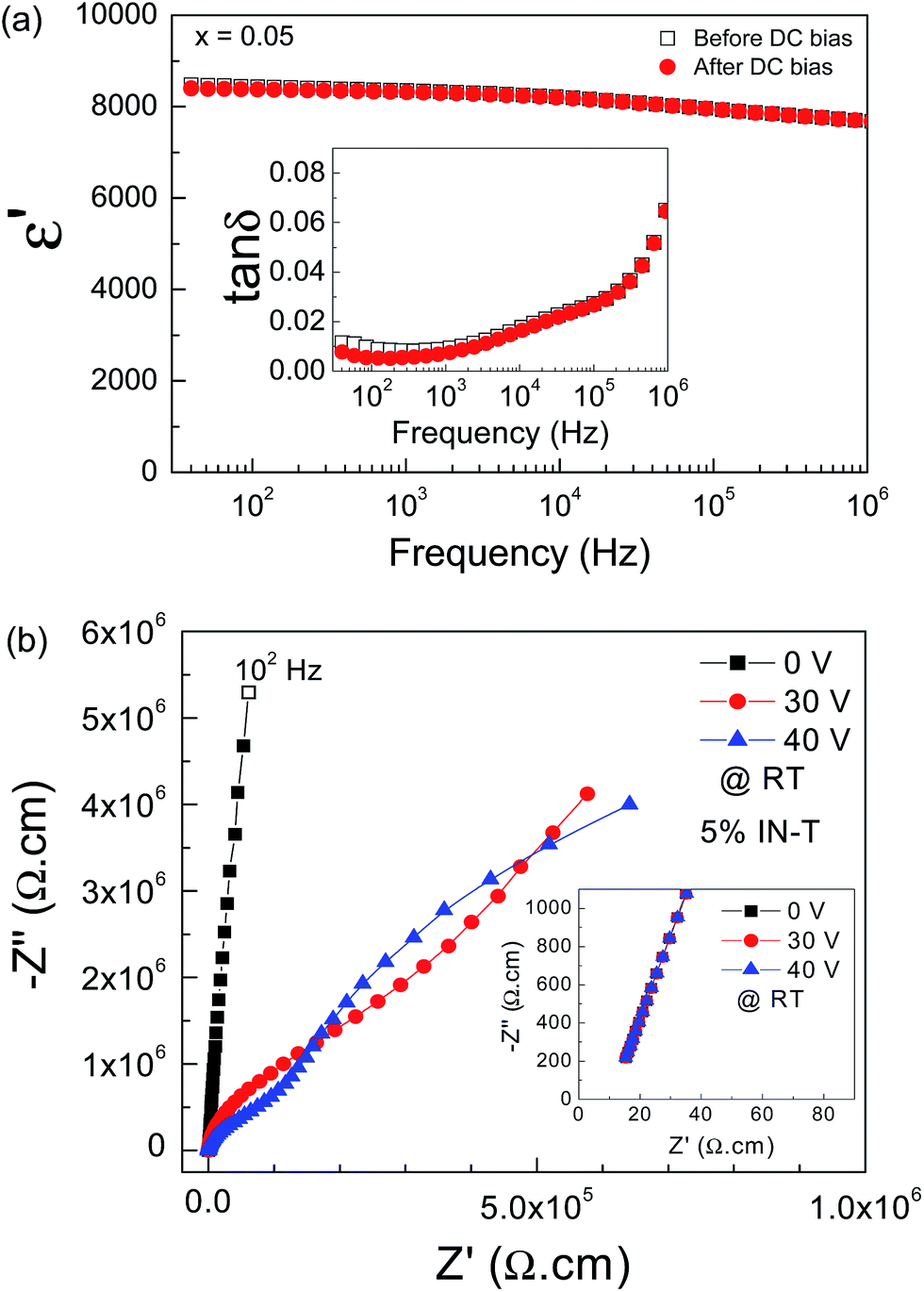 | ||
| Fig. 8 (a) ε′ of the 5% IN-T ceramic before and after an applied DC bias at 40 V (measured at RT without DC bias); inset shows tanδ before and after the applied DC bias at 40 V. (b) RT–impedance complex plane (Z*) plot under DC bias at 0, 30 and 40 V for the 5% IN-T ceramic; inset shows the nonzero intercept near the origin. | ||
To reveal the dielectric and electrical behavior of the 5% IN-T ceramic after OLM occurred, the dielectric measurement under different DC bias voltages was carried out at higher temperatures. At 50 °C, the dielectric properties can be measured only in the range of 0–35 V, and OLM occurred when the DC bias was adjusted to 40 V. The frequency dependence of ε′ at 50 °C under an applied DC bias (0–35 V) for the 5% IN-T ceramic is demonstrated in Fig. 7(b). For any DC bias voltage level, the induced step-like decrease in ε′ shifted to a high frequency when the temperature was increased from RT to 50 °C. In addition, a linear increase in ε′ in the frequency range below 100 Hz was dominant, which corresponds to a large increase in tanδ as frequency decreased [inset of Fig. 7(b)]. The relaxation tanδ peak is not observed, which is likely due to the great effect of DC conduction. Energy loss (tanδ) due to the dielectric relaxation phenomenon was concealed by very high energy loss contributed from the DC conductivity (σdc).
The dielectric properties of the 5% IN-T ceramic at RT without DC bias before and after OLM with different types of electrodes are depicted in Fig. 7(c) and (d). After OLM occurred at 50 °C, for 15 h, an additional ε′ plateau at RT for the 5% IN-T ceramic with an Au-sputtered electrode was observed in a low-frequency range, while the primary dielectric response did not change. The step-like decrease in ε′ was observed at ≈104 Hz. The overall dielectric behavior of the 5% IN-T ceramic after overload took place is quite similar to that observed in the 10% IN-T ceramic. By replacing the Au sputtered electrode with an Ag paint electrode (the sample thickness did not change and the outer surface layer was not removed), the dielectric spectrum over the measured frequency range is similar to that obtained from the Au-sputtered electrode; however the magnitude of the dielectric response was lower [Fig. 7(c)]. The difference in the magnitudes of the dielectric responses between the samples with Au sputtered and Ag paint electrodes is primarily due to the utilization of different methods for electrode preparation. Although the electrodes are fabricated from the same metal, the dielectric response of the sample with the sputtered electrode is usually larger.30 This means that the induced-LFCDR in the frequency range of 40 to 104 Hz may primarily be correlated with another source (e.g., the interface between the resistive outer-surface layer and conductive inner core), whereas the electrode polarization effect cannot be ignored.
Two different dielectric behaviors were observed in the 5% IN-T and 10% IN-T ceramics. First, in the low-frequency range of 40–300 Hz, a linear increase in ε′ appears, which indicates another source of polarization. Second, the induced relaxation tanδ peak is not observed. These results indicate a strong dominant effect of DC conductivity, which is usually related to an electrode effect. The low-frequency tanδ of the 5% IN-T ceramic using the Ag paint electrode is much lower than that of the ceramic using the Au sputtered electrode by about 2 orders of magnitude. Furthermore, a relaxation tanδ peak is observed. This means that the interface resistance (Re) of the ceramic with the Ag paint electrode is much larger than that of the ceramic with the Au-sputtered electrode. After OLM, it is possible that some free charges were trapped at the sample–electrode interface. This produced electrode polarization, which is generally accompanied with a very larger tanδ value.
To confirm the dielectric response of each source of polarization in the 5% IN-T ceramic, combined Z′′ and M′′ spectroscopic plots at RT were used. As shown in Fig. 9(a), without DC bias, Z′′ and M′′ peaks of an insulating phase(s) are not observed because they are at <40 Hz. The M′′ peak of the semiconducting phase is at >10 MHz, which is clearly assigned to the semiconducting grains. Careful inspection suggests that there is an intermediate component phase (referred to as phase 1) present with fmax between 104 and 105 Hz, as indicated by the M′′ shoulder-peak in the dash rectangular area. At 30 V DC bias, another M′′ peak appeared with fmax = 95.5 Hz (not shown), while the Z′′ peak still disappeared. As demonstrated in Fig. 9(b), with an increase in the DC bias to 40 V, the fmax of the low-frequency M′′ peak shifted to 330 Hz (referred to as phase 2). Interestingly, the Z′′ peak was not observed, which was expected to exist at fmax < 40 Hz (referred to as phase 3). These results indicate that there are two insulating interfaces in the 5% IN-T ceramic, which occurred by applying DC bias.
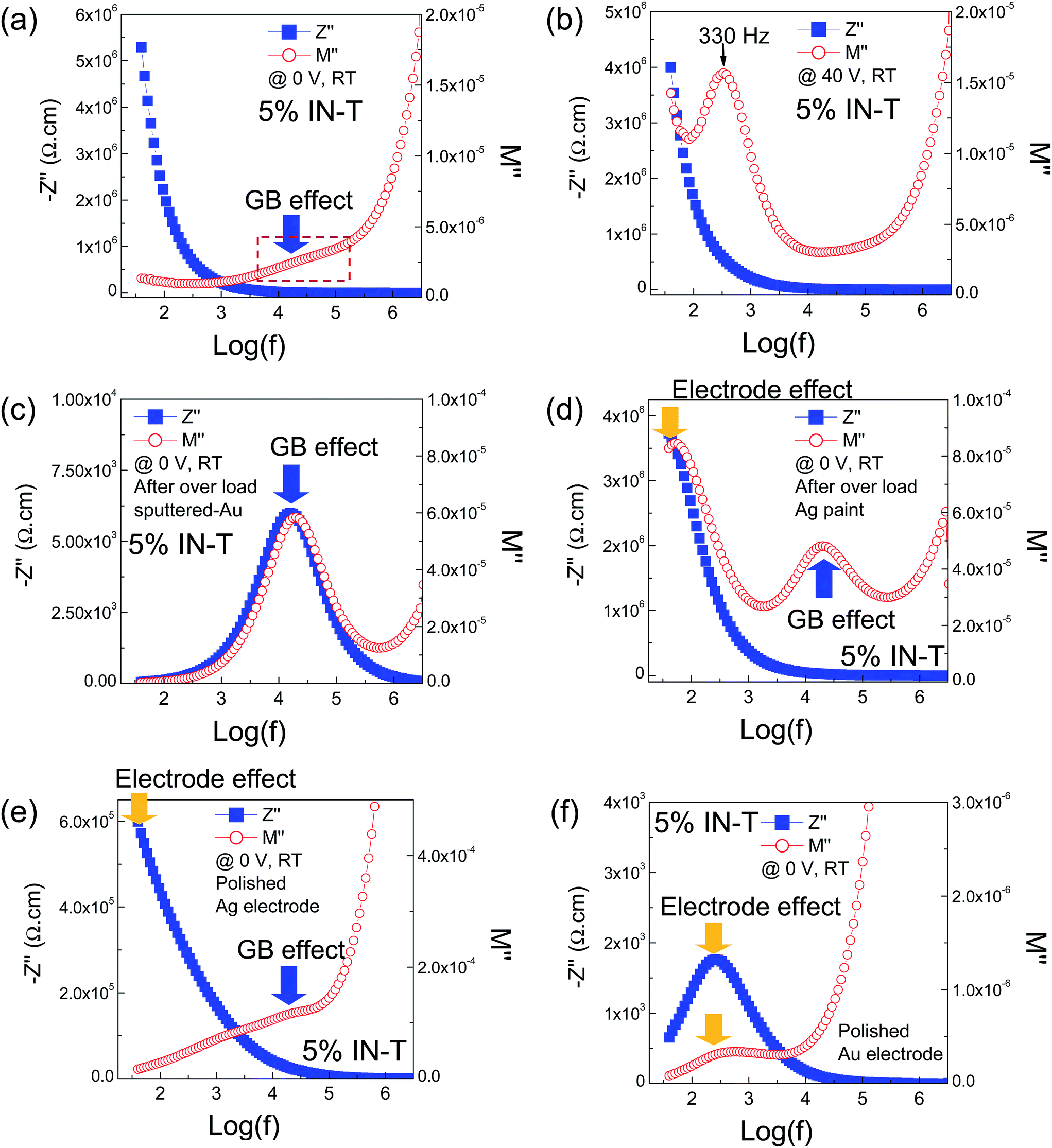 | ||
| Fig. 9 (a and b) Combined Z′′ and M′′ spectroscopic plots at RT for the as-fired 5% IN-T ceramic sample under 0 and 40 V DC bias, respectively. (c and d) Combined Z′′ and M′′ spectroscopic plots at RT without DC bias (0 V) for the 5% IN-T ceramic samples after an overload limited DC bias measurement using Au-sputtered and Ag paint electrodes, respectively. (e and f) Combined Z′′ and M′′ spectroscopic plots at RT without DC bias (0 V) for the polished 5% IN-T ceramic samples using Au-sputtered and Ag paint electrodes, respectively. | ||
As discussed earlier from Fig. 7, after OLM occurred, the electrical response of sample–electrode contact was much more dominant than that of the outer-surface layer effect. As shown in Fig. 9(c), both Z′′ and M′′ peaks appear at almost the same frequency with fmax between 104 and 105 Hz, which indicates that only phase 1 appeared in the measured frequency range after OLM. By replacing the Au sputtered electrode with the Ag paint electrode, both the peak height and peak position (fmax) of the M′′ peak for phase 1 did not change. Notably, the low-frequency Z′′ and M′′ peaks appeared at almost the same frequency with fmax ≈ 40–50 Hz. Clearly, phase 3 can be assigned as the electrical response of the sample–electrode contact, i.e., the electrode effect. Thus, phase 2 can be reasonably attributed to the resistive outer-surface layer response. It is possible that after OLM occurred at 50 °C, the insulating properties of the resistive outer-surface degraded and eventually became less dominant. After that, both surface sides of the 5% IN-T ceramic were removed by polishing. As depicted in Fig. 9(e), the low-frequency electrode response and phase 1 were still observed. This strongly confirms that phase 1 was the GBs. When the Au sputtered electrode was used, only the electrode effect could be observed, as shown in Fig. 9(f).
According to the experimental results in the present study, it is suggested that the primary polarization that gives rise to the high ε′ of IN-T ceramics is likely to be attributed to the interfacial polarizations. On the other hand, it is found that the most important factor contributing to a very low tanδ value (<0.05) is the resistive outer-surface layer. The resistive outer-surface is not only able to prevent DC conduction through the ceramic sample, but also inhibit the formation of a non-ohmic sample–electrode contact, which is usually accompanied with a large tanδ value in the low-frequency range. This gives rise to the high performance dielectric properties in IN-T ceramics. From the point of view of capacitor applications, according to our previous study,8 co-doping TiO2 with a high concentration of In + Nb (10%) causes a decrease in the temperature stability of ε′, and thus a low co-doping concentration was suggested. In the present study, we also suggest that the substitution of In + Nb co-dopants into TiO2 with a low concentration can cause the DC bias independence of the dielectric properties. Although the thickness of the resistive outer-surface layer cannot be calculated, this study provides an important alternative method to achieve a high dielectric performance in the IN-T ceramic system.
Finally, it should be noted that this study does not discredit the possibility of the electron pinned-defect dipole model generated by essentially designing complex defects in a rutile structure. The discussion is based on the experimental results obtained in our synthesized IN-T ceramics. Essentially, the special structure of complex defects may also possibly exist in our IN-T ceramics; however they were not found to dominate. Instead, the observed semiconducting grains might originate from the very large amount of free charges existing during the sintering step at a very high temperature of 1500 °C. In this case, the excess free electrons cannot be captured by the triangular shaped 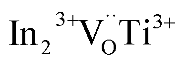 defect complexes.
4. Conclusion
The origin of the high-performance dielectric properties and optimized composition of co-doped TiO2 ceramics for suitable use in practical applications were successfully determined by studying the influences of DC bias on colossal dielectric responses. According to an analogous study of the DC bias effect in Nb single-doped TiO2 ceramics, the unique characteristics under DC bias for the dielectric responses contributed from the electrode and GB effects are clearly demonstrated. The low-frequency ε′ and tanδ of IN-T ceramics are strongly induced by applying DC bias and are removed by immediately applying no DC bias. It is demonstrated that the induced-polarization can permanently appear without DC bias by applying DC bias over the overload limited measurement. In all of the cases, the primary polarization remained unchanged. The permanent induced-polarizations originated from the dielectric responses of the non-ohmic sample–electrode contact and resistive outer-surface layer. The excellent dielectric performance of IN-T ceramics was shown to be primarily attributed to the existence of a resistive outer-surface layer, while the colossal dielectric response was originated from the interfacial polarization at the insulating GBs.
Acknowledgements
This study was financially supported by the Thailand Research Fund (TRF) and Khon Kaen University, Thailand [Grant Number RSA5880012]. The authors would like to thank the SUT-NANOTEC-SLRI (BL5.1) Joint Research Facility for use of their XPS facility and the P1551019 project from Environment Research Unit, National Metal and Materials Technology Center to partially support this study. W. Tuichai would like to thank the Thailand Graduate Institute of Science and Technology (TGIST) for his Ph.D. scholarship [Grant number SCA-CO-2558-1033-TH].References
- W. Hu, Y. Liu, R. L. Withers, T. J. Frankcombe, L. Norén, A. Snashall, M. Kitchin, P. Smith, B. Gong, H. Chen, J. Schiemer, F. Brink and J. Wong-Leung, Nat. Mater., 2013, 12, 821–826 CrossRef CAS PubMed.
- L. Singh, I. W. Kim, B. C. Sin, K. D. Mandal, U. S. Rai, A. Ullah, H. Chung and Y. Lee, RSC Adv., 2014, 4, 52770–52784 RSC.
- J. Li, K. Wu, R. Jia, L. Hou, L. Gao and S. Li, Mater. Des., 2016, 92, 546–551 CrossRef CAS.
- M. Gao, D. Feng, G. Yao, Y. Zhang, C. L. Chen and Y. Lin, RSC Adv., 2015, 5, 92958–92962 RSC.
- Z. Wang, Y. F. Wen, H. J. Li, M. R. Fang, C. Wang and Y. P. Pu, J. Alloys Compd., 2016, 656, 431–438 CrossRef CAS.
- H. Yang, Y. Yang, Y. Lin, J. Zhu and F. Wang, Ceram. Int., 2012, 38, 1745–1749 CrossRef CAS.
- J. Wu, C.-W. Nan, Y. Lin and Y. Deng, Phys. Rev. Lett., 2002, 89, 217601 CrossRef PubMed.
- W. Tuichai, S. Danwittayakul, S. Maensiri and P. Thongbai, RSC Adv., 2016, 6, 5582–5589 RSC.
- X.-G. Zhao, P. Liu, Y.-C. Song, A.-P. Zhang, X.-M. Chen and J.-P. Zhou, Phys. Chem. Chem. Phys., 2015, 17, 23132–23139 RSC.
- W. Dong, W. Hu, A. Berlie, K. Lau, H. Chen, R. L. Withers and Y. Liu, ACS Appl. Mater. Interfaces, 2015, 7, 25321–25325 CAS.
- Y. Q. Wu, X. Zhao, J. L. Zhang, W. B. Su and J. Liu, Appl. Phys. Lett., 2015, 107, 242904 CrossRef.
- T. Nachaithong, P. Thongbai and S. Maensiri, J. Eur. Ceram. Soc., 2017, 37, 655–660 CrossRef CAS.
- J. Li, F. Li, Y. Zhuang, L. Jin, L. Wang, X. Wei, Z. Xu and S. Zhang, J. Appl. Phys., 2014, 116, 074105 CrossRef.
- J. Li, F. Li, C. Li, G. Yang, Z. Xu and S. Zhang, Sci. Rep., 2015, 5, 8295 CrossRef CAS PubMed.
- Y. Song, X. Wang, Y. Sui, Z. Liu, Y. Zhang, H. Zhan, B. Song, Z. Liu, Z. Lv, L. Tao and J. Tang, Sci. Rep., 2016, 6, 21478 CrossRef CAS PubMed.
- Y. Song, X. Wang, X. Zhang, Y. Sui, Y. Zhang, Z. Liu, Z. Lv, Y. Wang, P. Xu and B. Song, J. Mater. Chem. C, 2016, 4, 6798–6805 RSC.
- G. Liu, H. Fan, J. Xu, Z. Liu and Y. Zhao, RSC Adv., 2016, 6, 48708–48714 RSC.
- C. Wang, N. Zhang, Q. Li, Y. Yu, J. Zhang, Y. Li and H. Wang, J. Am. Ceram. Soc., 2015, 98, 148–153 CrossRef CAS.
- Y. Y. Liu, X. M. Chen, X. Q. Liu and L. Li, Appl. Phys. Lett., 2007, 90, 262904 CrossRef.
- T. Adams, D. Sinclair and A. West, Phys. Rev. B: Condens. Matter Mater. Phys., 2006, 73, 094124 CrossRef.
- M. Li, D. C. Sinclair and A. R. West, J. Appl. Phys., 2011, 109, 084106 CrossRef.
- M. Li, A. Feteira and D. C. Sinclair, J. Appl. Phys., 2009, 105, 114109 CrossRef.
- P. Thongbai, T. Yamwong and S. Maensiri, Appl. Phys. Lett., 2009, 94, 152905 CrossRef.
- K. Meeporn, N. Chanlek and P. Thongbai, RSC Adv., 2016, 6, 91377–91385 RSC.
- J. Li, Z. Xu, F. Li, X. Zhu and S. Zhang, RSC Adv., 2016, 6, 20074–20080 RSC.
- P. Lunkenheimer, S. Krohns, S. Riegg, S. G. Ebbinghaus, A. Reller and A. Loidl, Eur. Phys. J.: Spec. Top., 2010, 180, 61–89 CrossRef.
- R. Schmidt, M. C. Stennett, N. C. Hyatt, J. Pokorny, J. Prado-Gonjal, M. Li and D. C. Sinclair, J. Eur. Ceram. Soc., 2012, 32, 3313–3323 CrossRef CAS.
- K.-C. Kao, Dielectric phenomena in solids: with emphasis on physical concepts of electronic processes, Academic Press, Amsterdam, Boston, 2004, vol. xvii, p. 581 Search PubMed.
- M. Li, Z. Shen, M. Nygren, A. Feteira, D. C. Sinclair and A. R. West, J. Appl. Phys., 2009, 106, 104106 CrossRef.
- S. Krohns, P. Lunkenheimer, S. G. Ebbinghaus and A. Loidl, J. Appl. Phys., 2008, 103, 084107 CrossRef.
| This journal is © The Royal Society of Chemistry 2017 |