
 Open Access Article
 This Open Access Article is licensed under a
 Creative Commons Attribution 3.0 Unported Licence
Study on the efficient PV/TE characteristics of the self-assembled thin films based on bismuth telluride/cadmium telluride
Vivekanandan Ramana,
Dinah Punnoosea,
Pari Baraneedharanb,
Sunkara Srinivasa Raoa,
Chandu V. V. M. Gopia,
Venkatesh Sc,
S Brahadeeswarand and
Hee-Je Kim *a
*a
aDepartment of Electrical and Computer Engineering, 2, Busandaehak-ro 63 beon-gil, Geumjeong-gu, Busan 46241, Korea. E-mail: heeje@pusan.ac.kr
bAlternative Energy and Nanotechnology Laboratory, Indian Institute of Technology Madras, Chennai, 600036, India
cDepartment of Physics, Indian Institute of Science, Bangalore, India
dDepartment of Physics, Anna University BIT Campus, Tiruchirappalli, Tamilnadu, India
First published on 20th January 2017
Abstract
Solar radiation has a spectral distribution ranging from short wavelengths (200–800 nm, visible part) to long wavelengths (800–3000 nm, heat part). Cadmium telluride and bismuth telluride are well known photovoltaic (PV) and thermoelectric (TE) materials, respectively. CdTe converts light energy into electricity and Bi2Te3 converts heat into electricity. To effectively use the entire solar spectrum for energy conversion, a new type of solar cell based on a Bi2Te3/CdTe composite in a core/shell structure was designed and prepared using a wet chemical method. X-ray diffraction and high-resolution transmission electron microscopy confirmed the formation of Bi2Te3/CdTe in a core/shell structure with high crystallinity. Bi2Te3 nanoparticles function as built-in nanoscale electron generators to convert heat into electricity and CdTe functions as a photovoltaic cell. The efficiency of the thin film solar cell device was found to be 2.5% at room temperature and 4.8% when exposed to sunlight. The combined PV and TE modules resulted in an overall power conversion efficiency of 4.8%.
1. Introduction
Solar energy is the cleanest and the most abundant renewable energy source available. CdTe, CuIn(Ga)Se2, and c-Si are advanced materials that are used as absorber materials in solar cells.1 Although these materials have high efficiency, the lack of abundance, high toxicity levels, and high production costs are problems that have prompted researchers to search for new materials and/or newer and easier synthesis routes. Therefore, continuous efforts are being made to find new, cost-effective photovoltaic materials with good conversion efficiency. Solar radiation has a spectral distribution from the short wavelength range, 200–800 nm (light part), to the long wavelength range, 800–3000 nm (heat part). Better control of light scattering and electronic transport through a semiconductor is crucial for improving the solar efficiency. Photovoltaic cells (PV), such as CdTe, can only convert the short wavelengths of solar energy into electricity and the remaining long wavelength solar radiation is waste heat. Thermoelectric materials (TE), such as Bi2Te3, convert the waste heat into electricity. Bi2Te3 has a high Seebeck coefficient and can generate electricity, even at room temperature.2 Considerable efforts have been made to combine both PV and TE technologies to maximally utilize the entire solar spectrum. These hybrid technologies that combine the modules of PV and TE cannot solve the problems of solar energy synergy utilization at the material level because the functions of PV and TE modules are independent of each other. On the other hand, it will be beneficial if both the PV and TE functions can be achieved in a single material. If this single material can be prepared in a nanostructure, it will be more efficient. Nanoparticles of CdTe have good photoluminescence properties and have been used in the production of solar cells. CdTe nanoparticles are prepared via aqueous and non-aqueous synthesis routes. Compared to non-aqueous synthesis, aqueous synthesis is more reproducible, cheaper, and less toxic. In addition, the prepared samples are more water-soluble and bio-compatible.3 To prepare nanorods, a seed-mediated growth technique was performed, in which the precursor was added dropwise and the capping agent assisted in the growth of nanorods.4,5 This study reports the integration of photovoltaic CdTe and thermoelectric Bi2Te3 materials into a single photoelectrode in the form of a core/shell nanostructure. Interestingly, this material showed a conversion efficiency of 4.8% when exposed to sunlight.Core/shell nanorods have been produced by a layer-by-layer self-assembly method. This is an effective technique for the construction of well-defined nanostructures. Hengguo Wang et al. reported that the LBL technique is facile and relatively controllable and they confirmed the incorporation of Fe3O4 and quantum dots (QDs) into a single structure. The shell produced by this method is meant to be a functional hybrid nanoshell.6–9 The alternating adsorption of oppositely charged materials gives rise to a layer-by-layer (LBL) self-assembly deposition method, through which hydrogen-bonding interactions and electrostatic forces hold the nanostructures assembly together.10–12 The aim of developing Bi2Te3/CdTe core shell nanorods is to harvest electricity from both thermal energy and light energy produced by the sun. Jie Yang et al. proposed that self-assembled Bi2Te3/CdTe nanosheets showed an increase in the thermoelectric performance of Bi2Te3 due to the addition of CdTe, thus reaching a Seebeck coefficient of −182.2 μV K−1 at 300 K, which is slightly higher than that of the bulk Bi2Te3 sample, −180.0 μV K−1. This clearly shows that CdTe will also enhance the thermoelectric performance of Bi2Te3. Solar cells based on nanoparticles have higher solar efficiency because of their large surface area.13 Therefore, the increase in the surface area of planar nanorod carpets has been proposed to enhance solar light harvesting.14–16
2. Experimental section
2.1 Materials
All chemicals, such as bismuth(III) nitrate pentahydrate (Bi(NO3)3·5H2O), tellurium powder (Te), potassium hydroxide (KOH), polyvinyl alcohol (PVA), cadmium sulphate (CdSO4), and sodium borohydride (NaBH4), were purchased from Aldrich and used without further purification.2.2 Synthesis of Bi2Te3/CdTe core shell thin film nanostructures
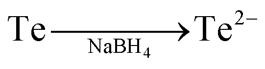
The front conductor influences the conductivity and plays a large role in the performance of a solar cell. An increase in the carrier mobility in the conductive FTO transparent conducting oxide layer provides lower absorptivity and lower resistivity.17 A FTO is properly cleaned to avoid weak adhesion, whereas a coating of CdS is deposited on the surface of the FTO. Acid exposure of the FTO will compromise the uniform deposition of CdS and affect the performance of the solar cell.18 CdS has high band width (2.4 eV) and acts as a windows layer for the cells, which plays a vital role in observing sunlight. In a clean FTO glass substrate, a three layer coating was deposited. The FTO substrate was masked and a 50–100 nm CdS layer was coated by thermal vapor deposition and annealed at 250 °C for 10 minutes. The CdS coating thickness affects the performance of the solar cell. The CdS should be thick enough because interdiffusion is promoted by the CdCl2 washing at the end of the deposition. The interdiffusion usually takes place without CdCl2. It has negative effects on cell operation. When the interdiffusion is strong enough, the light current is decreased. It has been claimed that a narrow interdiffusion of less than 100 nm between CdS and CdTe allows the smoother transition between both lattices, which should relax the surface states. When the thickness increases, the photo current decreases and absorption occurs.19 During the deposition of Bi2Te3/CdTe, interdiffusion between CdTe and CdS occurred. Moreover, CdS should be thick enough to not to be fully consumed by CdTe.20 Bi2Te3/CdTe core/shell nanorods were prepared by a wet chemical method. Bismuth(III) nitrate pentahydrate (0.04 mol) was placed in 10 mL of double-distilled water (DDW). Tellurium (0.06 mol) in 10 mL of DDW was mixed with bismuth nitrate solution and stirred. Subsequently, 0.5 mol of KOH was added to the abovementioned solution after 5 min. The CdS-coated FTO substrate was then immersed in the prepared solution. About 0.04 mol of the reducing agent, NaBH4, was added dropwise to reduce the bismuth nitrate and tellurium to bismuth telluride nanoparticles.21 The reducing agent is oxidized because it loses electrons in the redox reaction. The first step involves the reduction of Bi(NO3)3·5H2O and tellurium. When H2O is added to Bi(NO3)3·5H2O, salt separates into Bi3+ and 6NO− ions, whereas in the case of Te powder, Te changes into Te2−. When NaBH4 is added, these ions form clusters. In the second stage, the clusters coalesce to produce small particles with radius of 20–50 nm. This is followed by a metastable state, where the particles maintain the constant size for around 5–10 min. After 10–20 min, the last coalescence phase takes place to generate final Bi2Te3 nanoparticles about the size of 150–250 nm.
| 3Te2− + 2Bi3+ → Bi2Te3 |
When NaBH4 is added followed by stirring, nanorods of Bi2Te3 are formed via a self-assembly mechanism. Herein, in the self-assembly mechanism, at the critical concentration, the molecules start to interact with each other resulting in the nucleation of crystals. Using hydrogen bonding and electrostatic or ionic forces, Bi2Te3 clusters with itself to form nanorods. When PVA is added, it bonds to Bi2Te3. PVA plays a critical role in bonding Bi2Te3 and CdTe. PVA attracts the CdTe nanoclusters due to hydrogen bonding and forms core/shell nanorods, as shown in Fig. 1. A 0.1 g sample of polyvinyl alcohol (PVA) was added to the Bi2Te3 solution under stirring to form bonds with the Bi2Te3 nanoparticles. After 30 min of heating at 70 °C, the polymer PVA transformed the Bi2Te3 nanoparticles into nanorods, and the solution turned black and coated the CdS substrate. Cadmium sulfate and tellurium were then mixed in 20 mL of DDW with 0.04 and 0.06 molarity, respectively, and stirred well for 20 min. The solution was then poured into the Bi2Te3 nanorods solution, where CdTe forms a shell over Bi2Te3. The polymer plays a crucial role in reducing CdTe to nanoparticles and attaching over Bi2Te3. This mixture was kept at 70 °C and stirred well for 30 min. CdTe was coated over Bi2Te3 and the substrate was washed with CdCl2 and distilled water, and then dried and annealed at 400 °C for 4 h. This procedure was followed to prepare different concentrations of bismuth telluride with cadmium telluride at ratios of 1![[thin space (1/6-em)]](https://www.rsc.org/images/entities/char_2009.gif) :3, 1:1, and 3:1. Annealing at high temperatures encourages CdS/CdTe interdiffusion during growth, larger grain size, and generally provides a higher Voc.22 This Bi2Te3/CdTe will act as a p-type semiconducting layer, whereas CdS will act as an n-type semiconducting layer. Therefore, these two layers form a p–n junction. The back contact was coated with gold to reduce the resistance and increase the performance. A Cu wire was separately attached to the FTO and gold contact to complete the circuit.20
:3, 1:1, and 3:1. Annealing at high temperatures encourages CdS/CdTe interdiffusion during growth, larger grain size, and generally provides a higher Voc.22 This Bi2Te3/CdTe will act as a p-type semiconducting layer, whereas CdS will act as an n-type semiconducting layer. Therefore, these two layers form a p–n junction. The back contact was coated with gold to reduce the resistance and increase the performance. A Cu wire was separately attached to the FTO and gold contact to complete the circuit.20
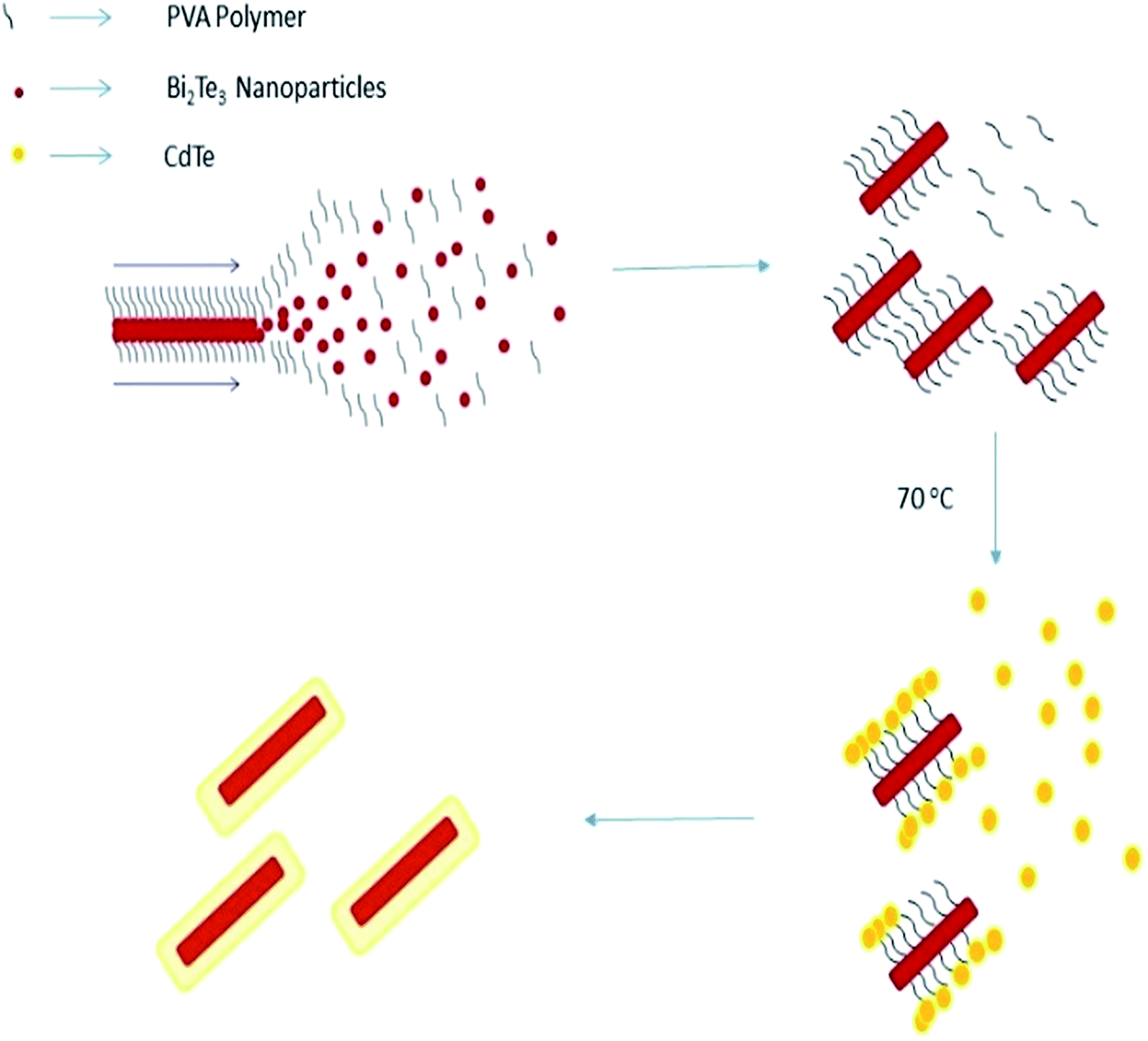 | ||
| Fig. 1 Self-assembly of Bi2Te3/CdTe with the help of a PVA polymer. | ||
2.3 Characterization
The phase identification of (Bi2Te3)75(CdTe)25, (Bi2Te3)50(CdTe)50, and (Bi2Te3)25(CdTe)75 was investigated using X-ray diffraction (XRD; Bruker D8-Advance) with a Cu-Kα radiation (λ = 1.540 Å) source operated at 40 kV and 30 mA in the range of 10–60°. The morphology of the sample was examined using high resolution transmission electron microscopy (HRTEM; Jem 2011, Jeol cop.) with a CCD 4k × 4k camera (Ultra Scan 400SP, Gatan cop.) at the Busan KBSI. X. The constituents and morphological changes of (Bi2Te3)75(CdTe)25, (Bi2Te3)50(CdTe)50, and (Bi2Te3)25(CdTe)75 and the elemental compositions of the samples were examined using a field emission scanning electron microscope (FE-SEM, SU-70, Hitachi) operated at 10.0 kV with an energy-dispersive X-ray spectroscopy (EDX) operated at 15 kV. The diffuse reflection of absorption spectra of (Bi2Te3)75(CdTe)25, (Bi2Te3)50(CdTe)50, and (Bi2Te3)25(CdTe)75 was obtained using an Optizen 3220 UV spectrophotometer. The photocurrent density–voltage characteristics of the thin film solar cell were obtained under one-sun illumination (AM 1.5G, 100 mW cm−2) using an ABET Technologies (USA) solar simulator with an irradiance constancy of ±3%.3. Results and discussions
X-ray diffraction (XRD) revealed that the observed peaks corresponded to rhombohedral Bi2Te3 (JCPDS, 73-2036) and the XRD pattern matched that of the JCPDS-89-3011 for the cubic CdTe in planes 200 and 111,23 with a composition ratio of (Bi2Te3)25(CdTe)75, (Bi2Te3)75(CdTe)25, and (Bi2Te3)50(CdTe)50. The crystalline nature of Bi2Te3 and CdTe indicates the broadening of the XRD peaks in the form of nanoparticles.24 The XRD peaks suggest that the size of the Bi2Te3/CdTe particle material is small ranging from 200 to 250 nm, which was observed from the broad peaks.25 Interestingly, Fig. 2 shows that for (Bi2Te3)75 (CdTe)25, the XRD peaks corresponding to Bi2Te3 are more intense than those corresponding to CdTe, whereas for (Bi2Te3)25(CdTe)75, the peaks corresponding to CdTe are dominant. The XRD pattern of (Bi2Te3)50(CdTe)50 closely matches that of (Bi2Te3)75(CdTe)25. This suggests that the crystalline phase ratio between Bi2Te3 and CdTe can be controlled by optimizing the ratio between Bi2Te3 and CdTe.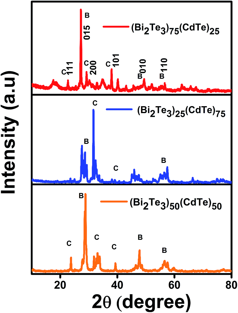 | ||
| Fig. 2 XRD patterns of Bi2Te3/CdTe powder composites. XRD data for comparison of bismuth telluride percentage in cadmium telluride. | ||
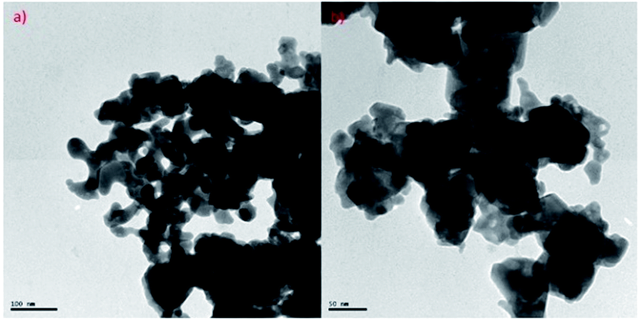
Transmission electron microscopy (TEM) of annealed Bi2Te3/CdTe revealed the formation of nanorods with sizes in the range of 100–250 nm (Fig. 3(a)). Fig. 3(b) clearly shows the core shell nanostructure of (Bi2Te3)25(CdTe)75. The selected area electron diffraction (SAED) pattern in Fig. 3(c) and (d) revealed the crystalline structural complexity and the fringes of CdTe with a lattice spacing of 0.35 nm corresponding to the (111) cubic planes of CdTe crystals (as shown in Fig. 3(c)),26,27 and Bi2Te3 has a lattice spacing of 0.13 nm corresponding to (125) trigonal planes. (Bi2Te3)25(CdTe)75 clearly shows nanorod formation (Fig. 4(a) and (b)), whereas formation of nanorods does not occur in samples (Bi2Te3)75(CdTe)25 and (Bi2Te3)50(CdTe)50. In Fig. 5, the field emission scanning electron microscopy (FESEM) also reveals a morphology of (Bi2Te3)25(CdTe)75 exhibiting nanorod formation. The colloidal morphology was observed in the TEM and the outer morphology of the sample (Bi2Te3)25(CdTe)75 was observed by FESEM, which show that nanorods, approximately 240 nm in size, are present in the sample. The atomic ratio of Te to Bi to Cd obtained from the quantitative analysis of Te, Bi, and Cd in the EDX spectrum has an atomic weight percentage ratio of 40.90:9.99:49.11 and a weight percentage ratio for Te, Bi and Cd as 40.69:16.27:43.04, respectively, indicating that the ratio of (Bi2Te3)25(CdTe)75 is similar to the 25:75 ratio shown in Fig. 6.
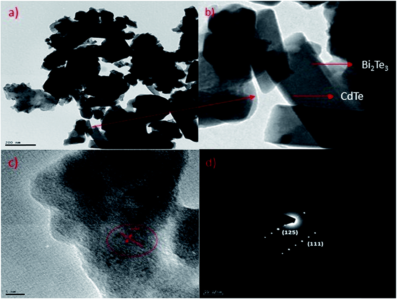 | ||
| Fig. 3 (a) & (b) Core/shell nanostructure of (Bi2Te3)25(CdTe)75; (c) & (d) electron diffraction (SAED) shows the crystalline structure of Bi2Te3/CdTe in sample (Bi2Te3)25(CdTe)75. | ||
 | ||
| Fig. 4 TEM images of powder samples of (a) (Bi2Te3)75(CdTe)25 and (b) (Bi2Te3)50(CdTe)50. | ||
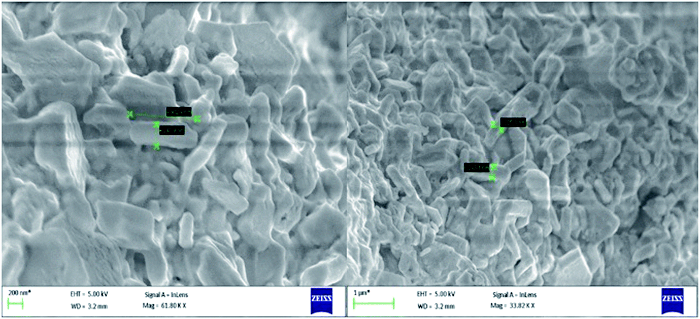 | ||
| Fig. 5 FESEM morphology of the sample (Bi2Te3)25(CdTe)75 having nanorods approximately 240 nm in size. | ||
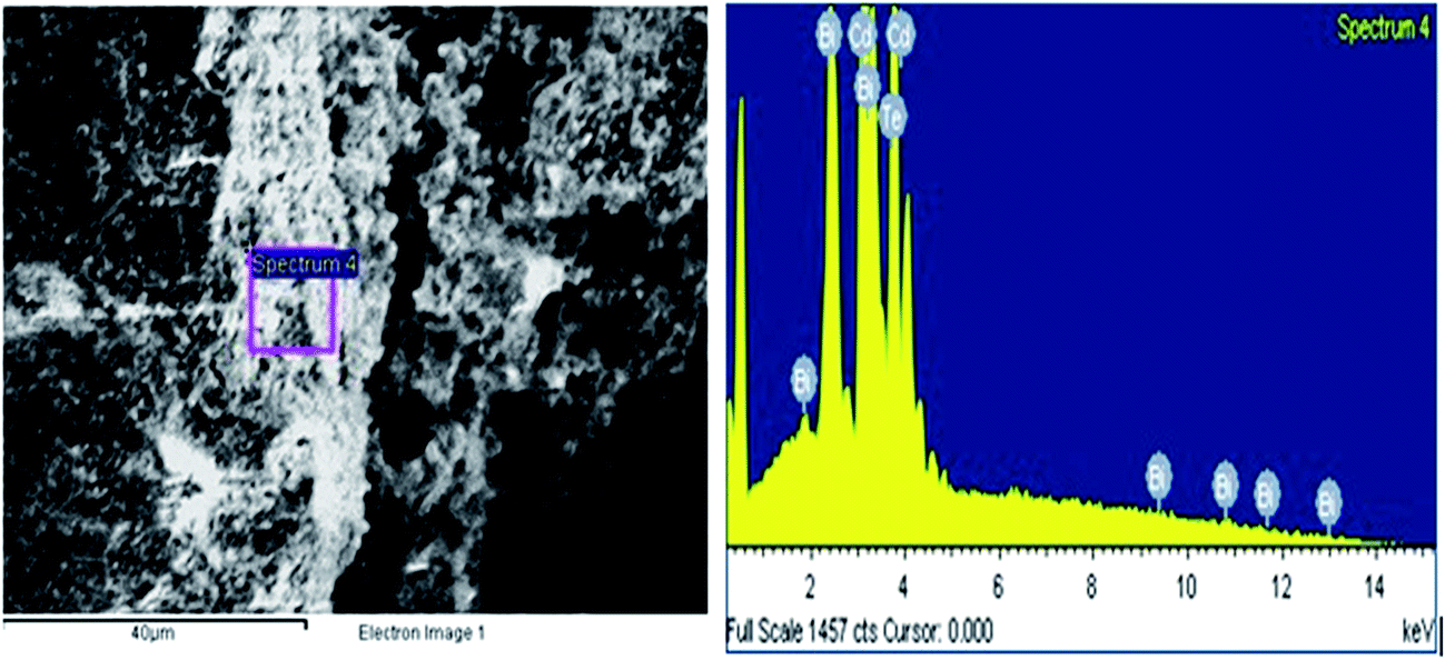 | ||
| Fig. 6 EDX spectrum of (Bi2Te3)25(CdTe)75 sample. | ||
The transmittance and reflectance shows the structure of the nanorods. In Fig. 7(a), the transmittance image obtained using an advanced polarization microscope shows the structure of nanorods with a 400× magnification. Fig. 7(b) presents the reflectance image, showing the dark-green colored core spots of Bi2Te3 inside the orange colored CdTe shell.
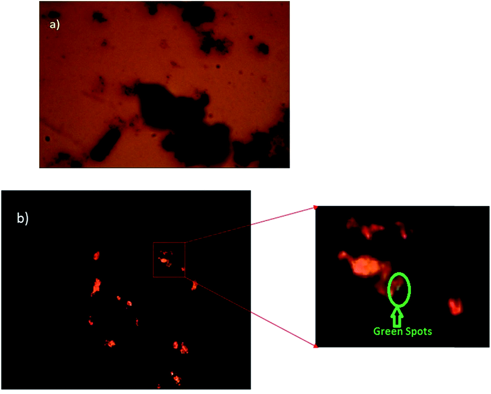 | ||
| Fig. 7 (a) Transmittance image of Bi2Te3/CdTe nanorods and (b) the reflectance image of Bi2Te3/CdTe nanorods. | ||
The energy band gap of the sample was obtained at different ratios. In (Bi2Te3)50(CdTe)50 sample, the bismuth telluride ratio is equal to that of CdTe. The energy band gap was 1.76 eV due to doping, resulting in a higher band gap. In combination with (Bi2Te3)75(CdTe)25, the proportion of bismuth telluride was greater than that of CdTe, resulting in a lower band gap of 1.25 eV. This shows that the concentration of bismuth telluride affects the energy band gap of cadmium telluride, which leads to a decrease in the efficiency of solar cells; however, in (Bi2Te3)25(CdTe)75, the ratio of bismuth telluride, influencing the energy band gap of CdTe, was very low (≈0.5%), such that the energy value of the sample was equal to the standard band gap of CdTe (1.44 eV).28–31 This shows that bismuth telluride with a ratio of (Bi2Te3)25(CdTe)75 does not affect the band gap of CdTe. Bi2Te3, which exhibits thermoelectric properties, only supports the increase in the solar cell efficiency and does not affect the band gap in the sample (Bi2Te3)25(CdTe)75. Moreover, (Bi2Te3)25(CdTe)75 has a band gap of 1.45 eV, as shown in Fig. 8. The band gap of CdS is 2.41 eV, which is similar to its standard band gap.
 | ||
| Fig. 8 The energy band gap graph of samples (a) (Bi2Te3)25(CdTe)75, (b) (Bi2Te3)75(CdTe)25, (c) (Bi2Te3)50(CdTe)50, and (d) CdS layer in the fabricated device. | ||
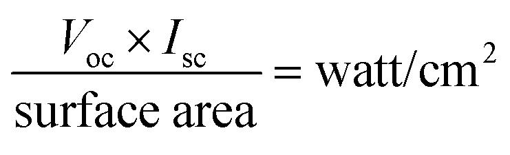
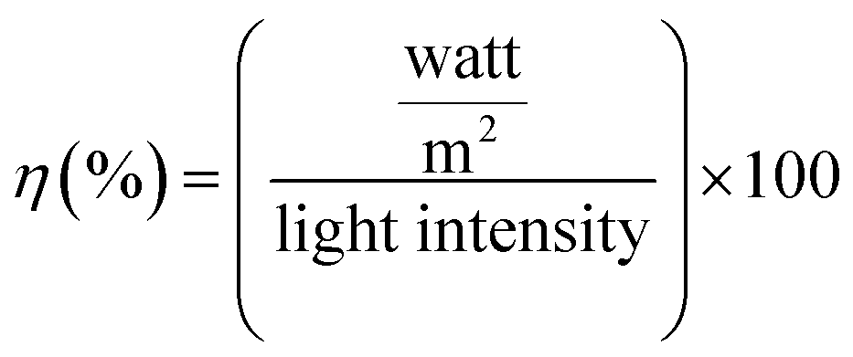
The effect of Bi2Te3 in the photoanode on the charge recombination kinetics was investigated by analyzing the I–V characteristics under sunlight at room temperature. Fig. 9 shows the output current and voltage to determine the efficiency of the solar cell. The calculation was performed as follows:
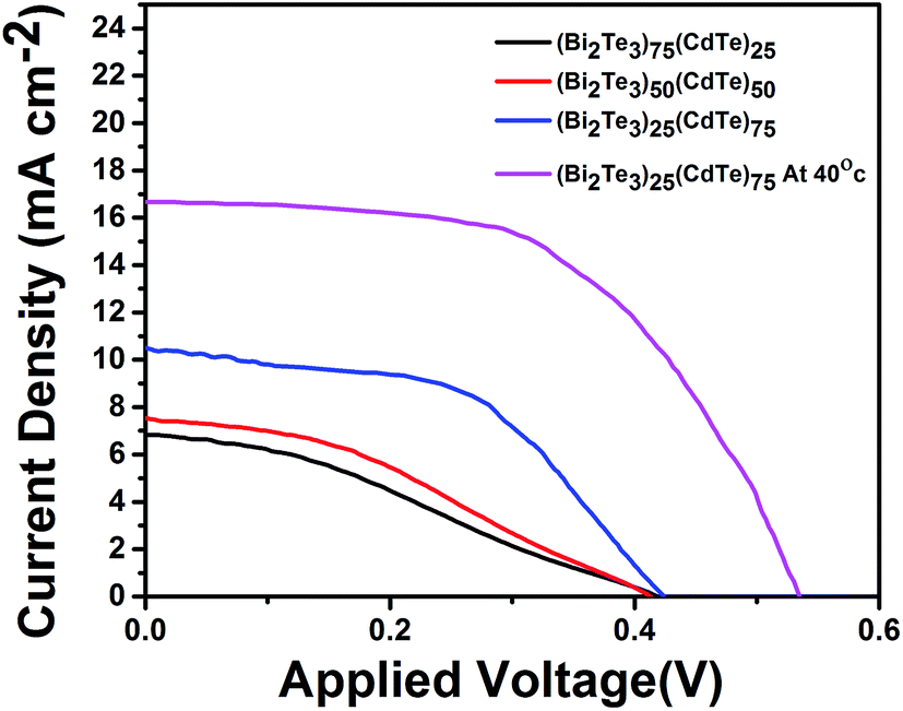 | ||
| Fig. 9 Light irradiation (one sun) graph showing duration-dependent I–V characteristics of the device. | ||
The intensity of light was 700 watt per m2
Bi2Te3, with a large thermoelectric figure of merit (ZT), is defined as σS2T/k, where σ is the electrical conductivity, S is the Seebeck coefficient or thermopower, T is the absolute temperature, and k is the thermal conductivity. Bi2Te3 has an enhanced ZT, a high Seebeck coefficient, an increased electrical conductivity, and a low thermal conductivity. The formation of acceptor and donor levels in the CdTe samples is associated with Bi concentration. The interdiffusion of Bi-doping with CdTe solar cells at lower concentration of Bi-doping makes BiCd+ to act as a donor. Therefore a higher Jsc in the sample (Bi2Te3)25(CdTe)75 was achieved as compared to that in the other concentration of Bi2Te3. This type of behavior is the mechanism of band bending at the GBs for CdTe solar cells with Bi2Te3.32 Large amount of positively charged BiCd+ donor accumulated near the GBs makes the band bending to occur. The photogenerated electron–hole pairs due to charge separation near GBs cause band bending. Electrons are attracted towards the GBs core (BiCd+) and flow through GBs, whereas the holes are transported through Cd to the back contact. A higher concentration of Bi2Te3 generates less power, thus lowering the efficiency. The efficiency was calculated for the combination of (Bi2Te3)75(CdTe)25 and (Bi2Te3)50(CdTe)50, where the higher concentration of Bi2Te3 makes the device unusable as a solar cell. Fig. 9 shows that (Bi2Te3)75(CdTe)25 has Jsc less when compared to the Jsc of (Bi2Te3)50(CdTe)50, denoting that the concentration of Bi2Te3 affects the efficiency of the solar cell. Carrier (holes) concentration in (Bi2Te3)75(CdTe)25 and (Bi2Te3)50(CdTe)50 decreases with the increase in Bi2Te3 weight ratio resulting from the lower antistructure defects due to the large difference in the electronegativity between Bi and Te. This causes a decrease in the electrical resistivity and Seebeck coefficient. As the concentration of Bi2Te3 is higher, the cells lose capability as solar cells and power conversion gets reduced. This impact results in lower Jsc and Voc. (Bi2Te3)75(CdTe)25 has Jsc of 7.273 and Voc of 0.41 mV with a lower fill factor of 29, which implies an efficiency of 0.89%. (Bi2Te3)25(CdTe)75 is observed to have higher Jsc when compared to that for other concentrations. The band gap of CdTe is not affected by the concentration of Bi2Te3 in (Bi2Te3)25(CdTe)75, thus having higher Jsc and Voc than the other two concentrations. Under conditions when the front side is illuminated, the power conversion efficiency of the solar cell with the FTO back contact was 2.27% with Voc = 0.42 mV, Jsc = 10.34 mA cm−2, and FF = 51.87% (Table 1).
| Condition | Voc (mV) | Jsc (mA cm−2) | FF | η (%) |
|---|---|---|---|---|
| (Bi2Te3)75(CdTe)25 | 419 | 7.273 | 29 | 0.89 |
| (Bi2Te3)50(CdTe)50 | 413 | 8.012 | 33 | 1.09 |
| (Bi2Te3)25(CdTe)75 | 423 | 10.34 | 51 | 2.27 |
| (Bi2Te3)25(CdTe)75 at 40 °C | 535 | 16.66 | 54 | 4.85 |
The sample (Bi2Te3)25(CdTe)75 shows a better efficiency when kept at 40 °C on a hot plate, similar to the temperatures found in tropical regions. When the sample reaches 40 °C, the I–V characteristics of the sample (Bi2Te3)25(CdTe)75 show an increase in the power conversion efficiency. As the temperature increases in the fabricated solar cell, the overall power conversion efficiency increases approximately by 2.5% in the presence of Bi2Te3 in the sample (Bi2Te3)25(CdTe)75. This shows that bismuth telluride in combination with cadmium telluride exhibits its thermoelectric property.33 This response to temperature suggests that bismuth telluride will make a huge difference in the solar cell efficiency in the near future. At 40 °C, the overall power conversion efficiency was 4.8%. The overall efficiency was increased by 24% when Bi2Te3 is in the composition ratio of 25% with CdTe.34
4. Conclusion
Bi2Te3/CdTe nanorods were synthesized using a wet chemical method. XRD and TEM revealed the mean particle size of Bi2Te3/CdTe material; XRD showed that an improvement in the crystallinity of the sample results after heat treatment. TEM revealed the formation of rod-shaped nanoparticles. Polarization microscopy revealed the presence of Bi2Te3 and CdTe confirming that Bi2Te3 and CdTe are in the form of core shell nanorods. The efficiency of the sample (Bi2Te3)25(CdTe)75 increased by 24% with respect to increase in temperature. The present study shows that Bi2Te3/CdTe doping can enhance the efficiency of the thin film CdTe solar cells.Acknowledgements
This work was supported by BK21PLUS, Creative Human Resource Development Program for IT Convergence. The authors would like to thank KBSI, Busan for SEM, TEM, XRD, and EDX analysis.References
- O. K. Varghese, M. Paulose and C. A. Grimes, Nat. Nanotechnol., 2009, 4, 592 CrossRef CAS PubMed.
- Encyclopedia of Nanoscience and Nanotechnology, ed. W. Chen, G. A. Joly, S. P. Wang and H. S. Nalwa, American Scientific Publishers, Los Angeles, CA, 2004, 4, pp. 689–718 Search PubMed.
- H. JyhGau, W.-R. Huang, C.-C. Wu, Y. Kang and C.-H. Ho, Solid State Phys., 2011, 170, 41 Search PubMed.
- N. R. Jana, L. Gearheart and C. Murphy, J. Phys. Chem. B, 2001, 105, 4065 CrossRef CAS.
- A. M. Alkilany, L. B. Thompson, S. P. Boulos, P. N. Sisco and C. J. Murphy, Adv. Drug Delivery Rev., 2012, 64, 190–199 CrossRef CAS PubMed.
- Y. Wang, L. Hosta-Rigau, H. Lomas and F. Caruso, Phys. Chem. Chem. Phys., 2011, 13, 4782 RSC.
- D. Y. Wang, A. L. Rogach and F. Caruso, Nano Lett., 2002, 2, 857 CrossRef CAS.
- F. Caruso and C. Schuler, Langmuir, 2000, 16, 9595 CrossRef CAS.
- G. Decher, Science, 1997, 277, 1232 CrossRef CAS.
- G. Decher, Science, 1997, 277, 1232 CrossRef CAS.
- W. B. Stockton and M. F. Rubner, Macromolecules, 1997, 30, 2717 CrossRef CAS.
- S. Sukhishvili and S. Granick, J. Am. Chem. Soc., 2000, 122, 9550 CrossRef CAS.
- E. Guillen, E. Azaceta, L. Peter, A. Zukal, R. Tena-Zaera and J. Anta, Energy Environ. Sci., 2011, 4, 3400 CAS.
- M. Law, L. E. Greene, J. C. Johnson, R. Saykally and P. D. Yang, Nat. Mater., 2005, 4, 455 CrossRef CAS PubMed.
- M. Quintana, T. Edvinsson, A. Hagfeldt and G. Boschloo, J. Phys. Chem. C, 2007, 111, 1035 CAS.
- J. B. Baxter and E. S. Aydil, Appl. Phys. Lett., 2005, 86, 053114 CrossRef.
- T. Coutts, X. Wu, P. Sheldon and D. Rose, 2nd IEEE World Photovoltaic Specialists Conference, Vienna, Austria, 1998 Search PubMed.
- D. H. Rose, F. S. Hasoon, R. G. Dhere, D. S. Albin, R. M. Ribelin, X. S. Li, Y. Mahathongdy, T. A. Gessert and P. Sheldon, Progress in Photovoltaics: Research and Applications, 1999, 7, 331–340 CrossRef CAS.
- J. Poortmans and V. Arkhipov, Thin Film Solar Cells Fabrication, Characterization and Applications, John Wiley & Sons Ltd, 2006 Search PubMed.
- I. O. Oladeji, L. Chow, C. S. Ferekides, V. Viswanathan and Z. Zhao, Solar Energy Materials & Solar Cells, 2000, vol. 61, pp. 203–211 Search PubMed.
- S. Gupta, S. Neeleshwar, V. Kumar and Y. Y. Chen, Adv. Mat. Lett., 2012, 3(1), 50–54 CrossRef CAS.
- X. S. Li, D. Albin, S. Asher, H. Moutinho, B. Keyes, R. Matson, F. Hasoon and P. Sheldon, AIP Conf. Proc., 1995, 353, 376–383 CrossRef.
- M. Melvin David Kumar and S. Devadason, Appl. Nanosci., 2013, 3, 453–459 CrossRef.
- I. H. Wang, L. Sun, Y. Li, X. Fei, M. Sun, C. Zhang, Y. Li and Q. Yang, Langmuir, 2011, 27, 11609–11615 CrossRef PubMed.
- H. Arizpe-Chavez, J. Phys. Chem. Solids, 2000, 61, 511–518 CrossRef CAS.
- I. H. Wang, L. Sun, Y. Li, X. Fei, M. Sun, C. Zhang, Y. Li and Q. Yang, Langmuir, 2011, 27, 11609–11615 CrossRef PubMed.
- J. Yang, Y. Gao, J. W. Kim, Y. He, R. Song, C. W. Ahn and Z. tang, Phys. Chem. Chem. Phys., 2010, 1238, 11900–11904 RSC.
- S. J. Fonash, Solar Cell Device Physics, Academic Press, New York, 1977 Search PubMed.
- A. L. Fahrenbruch and R. H. Bube, Fundamentals of Solar Cells, Academic Press, New York, 1983 Search PubMed.
- K. L. Chopra and S. R. Das, Thin Film Solar Cells, Plenum Press, New York, 1983 Search PubMed.
- A. Milnes and D. Feucht, Heterojunctions and Metal-semiconductor Junctions, Academic Press, New York, 1972 Search PubMed.
- R. Tang, Z. Wang, W. Li, L. Feng, J. Zhang, L. Wu, B. Li, G. Zeng and W. Wang, Sol. Energy Mater. Sol. Cells, 2014, 121, 92–98 CrossRef CAS.
- T. D. T. Ung, T. K. C. Tran, T. N. Pham, D. N. Nguyen, D. K. Dinh and Q. L. Nguyen, Adv. Nat. Sci.: Nanosci. Nanotechnol., 2012, 3, 043001 CrossRef.
- T. Chen, G. Hong Guai, C. Gong, W. Hu, J. Zhu, H. Yang, Q. Yan and C. M. Li, Energy Environ. Sci., 2012, 5, 6294–6298 CAS.
| This journal is © The Royal Society of Chemistry 2017 |