
 Open Access Article
 This Open Access Article is licensed under a
 Creative Commons Attribution 3.0 Unported Licence
Preparation of porous CuO films from Cu(NO3)2 aqueous solutions containing poly(vinylpyrrolidone) and their photocathodic properties†
H. Uchiyama *,
K. Isobe and
H. Kozuka
*,
K. Isobe and
H. Kozuka
Department of Chemistry and Materials Engineering, Kansai University, 3-3-35 Yamate-cho, Suita, 564-8680, Japan. E-mail: h_uchi@kansai-u.ac.jp; Fax: +81-6-6388-8797; Tel: +81-6-6368-1121 extn 5638
First published on 24th March 2017
Abstract
We prepared cupric oxide (CuO) photocathode films by dip coating from Cu(NO3)2 aqueous solutions containing poly(vinylpyrrolidone) (PVP). The addition of PVP modified the wettability of FTO glass substrates by the aqueous coating solutions, resulting in the formation of CuO coating layers on the substrates. The thermal decomposition of PVP by provided nanoscale pores in the resultant CuO films, and the porosity increased with increasing PVP content. The porous structure thus obtained led to an efficient photocathodic reaction under UV and visible light illumination (wavelength: 300–800 nm). Highly porous CuO films prepared at [PVP] = 0.25 M exhibited the maximum incident photon-to-current efficiency (IPCE) values of 8.7% and 3.9% at 300 and 500 nm, respectively.
Introduction
Cupric oxide (CuO), a p-type semiconductor, is a promising photoelectrode material due to its small band gap of 0.7–1.6 eV that enables solar light absorption, including visible light.1–7 A CuO photocathode has been reported that provides a theoretically a maximum photocurrent of 35 mA cm−2 under standard AM 1.5 irradiation5–9 and is superior to TiO2 (1.1 mA cm−2) and Fe2O3 (10.7 mA cm−2). However, it is difficult to achieve such a theoretical performance, and most of experimental studies of CuO photocathode films have demonstrated lower photocurrents. Thus, the improvement of the photoelectrochemical performance of CuO electrodes is urgently required.The control of the nanostructure of semiconductor electrodes is one of the typical strategies for enhancing the photoelectrochemical properties.1,10–15 Since the photoelectrochemical reactions occur on the surface of the electrode materials, a larger surface area of the nanostructured electrodes would result in more efficient energy conversion. Organic polymers are often used as a pore-forming agent for fabricating nanostructured metal oxide film materials.16–20 When large amounts of organic polymers are added into the precursor films, the organic species completely decompose on heat treatment, creating numerous nanoscale pores in the resultant metal oxide films. Liu et al. prepared ZnO thin films from Zn(CH3COO)2·2H2O solutions containing polyethylene glycol (PEG), wherein the ZnO films became porous with increasing PEG content in the precursor solutions.16 Yu et al. reported the preparation of porous TiO2 films from tetrabutylorthotitanate solutions containing PEG, wherein the addition of PEG led to the formation of a large number of pores in the resulting films, thus enhancing the photocatalytic activity.17 These results suggest that adding organic polymers as a pore-forming agent would allow us to fabricate porous CuO photocathode films and achieve an improvement in the photocathodic performance.
Previously, the preparation of metal oxide films by dip coating into coating solutions containing organic polymers with amide groups, such as poly(vinylpyrrolidone) (PVP), poly(vinylacetamide) and poly(acrylamide), has been reported.21 Organic additives were used for modifying the wettability of glass substrates by coating solutions, wherein homogeneous metal oxide films could be easily deposited onto the substrates even from aqueous solutions with a high surface tension. In those cases, however, we intended to make “dense” ceramic films, and thus only small amounts of organic polymers were added into the precursor solutions, and the influence of the additives on the microstructure of the films was not fully discussed. The addition of large amounts of organic polymers would lead to the formation of a porous structure in the resultant films, providing a higher photocathodic performance.
In this study, we prepared porous CuO photocathode films from Cu(NO3)2 aqueous solutions containing PVP, and evaluated their photocathodic properties. Herein, an organic polymer, PVP, was used for providing a porous structure in the CuO films, as well as for modifying the wettability of the glass substrates by the aqueous coating solutions. We investigated the effects of the PVP content in the solutions on the porosity of the CuO films. Moreover, the influence of the porous structure on the photoelectrochemical behavior was studied by measuring the current–potential curves and action spectra under the irradiation of xenon light.
Experimental
Preparation of porous CuO films
0–2.2 g of PVP (K90, 6.3 × 10⁵ in viscosity average molecular weight, Tokyo Kasei Kogyo Co., Tokyo, Japan) and 4.8 g of Cu(NO3)2·3H2O (Wako Pure Chemical Industries, Osaka, Japan) were added and dissolved in 40 cm3 of purified water under stirring at room temperature. The resultant blue solutions served as coating solutions ([Cu(NO3)2·3H2O] = 0.50 M, [PVP] = 0–0.50 M), where the concentration of PVP was defined for the monomer (polymerizing unit).Precursor films were deposited on the FTO (fluorine doped tin oxide) glass substrates (20 mm × 40 mm × 1.0 mm) by dip-coating, where the substrates were withdrawn at 3 cm min−1. The precursor films were directly transferred to an electric furnace held at 600 °C, and then maintained for 10 min; furthermore, they were removed and maintained at ambient atmosphere. The heat treatments on gel films were performed in air. The dip coating and heat treatment were repeated 1–10 times, and the resultant films were used as samples.
Characterization
The crystalline phases were identified by X-ray diffraction (XRD) measurements by ordinary 2θ/θ scan (coupled mode) using an X-ray diffractometer (Model Rint 2550V, Rigaku, Tokyo, Japan) with CuKα radiation operated at 40 kV and 300 mA. The chemical composition was measured by X-ray photoelectron spectroscopy (XPS) analysis (PHI 5000 Versa Probe, ULVAC-PHI, Kanagawa, Japan). The microstructure of the thin film samples was observed using a field emission scanning electron microscope (FE-SEM) (Model JSM-6500F, JEOL, Tokyo, Japan). The film thickness was also evaluated from the FE-SEM cross-sectional images of the samples. Optical transmission spectra were measured on the film samples using an optical spectrometer (V-570, JASCO, Tokyo, Japan), where an FTO glass substrate was used as a reference.Measurement of the photocathodic properties
Photocathodic properties of the CuO films were evaluated in a three-electrode cell using a potentiostat (HZ-7000, Hokuto Denko, Osaka, Japan) consisting of the film electrode sample, a platinized Pt electrode, and a saturated calomel electrode (SCE) as the working, counter, and reference electrodes, respectively, and a buffer solution of pH 7, an aqueous solution of 0.2 M Na2B4O7, 0.14 M H2SO4, and 0.3 M Na2SO4, as the supporting electrolyte.For measuring the current–potential curves, the potential of the working electrode was scanned from 0.1 to −0.5 V vs. SCE at a rate of 20 mV s−1. A 500 W xenon lamp (model UXL-500-D-0, XB-50101AA-A, UI-502Q, Ushio Denki, Tokyo, Japan) was used as the white light source where the light intensity was reduced to 30 mW at a wavelength of 550 nm using an ND filter. The film was illuminated for 5 s, and the light was turned off for 5 s. The light turning on and off was repeated during the scanning of the working electrode potential.
Action spectra of the films were measured at −0.1 V vs. SCE, where the xenon lamp light was monochromatized using a monochromator (SPG-100s, Shimadzu, Kyoto, Japan). The intensity of the monochromatized light was measured using a power meter (NOVA, PD300-UV, Ophir Japan, Saitama, Japan), which was ca. 23 μW at a wavelength of 500 nm. For this measurement, the film was first illuminated for 10 s, and then the light was turned off. The difference in current before and after turning off the light was taken as the photocurrent. Quantum efficiency and IPCE (incident photon-to-current efficiency) was calculated from the photocurrent and the incident light intensity.
Results and discussion
Preparation of CuO films from the coating solutions of various PVP contents
CuO precursor films were deposited onto FTO glass substrates from the coating solutions of [PVP] = 0–0.50 M by dip coating at 3.0 cm min−1. No films were formed on the substrates when no PVP was added in the solutions ([PVP] = 0 M), whereas CuO precursor films were obtained from the solutions of [PVP] = 0.05–0.50 M. This suggests that the wettability of the FTO glass substrates by Cu(NO3)2 aqueous solutions was improved by the addition of PVP.21The CuO precursor films thus obtained ([PVP] = 0.05–0.50 M) were heat-treated at 600 °C for 10 min in air to obtain CuO films, where the dip coating and the heat treatment were repeated 1–10 times. Crack-free, black-colored films were obtained at [PVP] = 0.05–0.40 M (ESI Fig. S1†). On the other hand, when a larger amount of PVP was added ([PVP] = 0.50 M), the decomposition of much organic species during the heating resulted in cracking and delamination of the films. The thickness of the crack-free CuO films prepared at [PVP] = 0.05–0.40 M by repeating the dip coating and the heat treatment is shown in Table 1. The thickness of the films increased with increasing cycling numbers and PVP content. We chose the CuO films of 210–250 nm in thickness as the electrode samples for the photoelectrochemical measurements so that the photocathodic properties were compared between films of similar thickness. Hereafter, the CuO electrode samples of 210–250 nm in thickness prepared at [PVP] = 0.05–0.40 M were denoted as films PVP0.05–0.40, respectively, as shown in Table 2.
Characterization and photoelectrochemical evaluation of CuO films
Fig. 1 shows the SEM images of films PVP0.05–0.40. CuO coating layer consisting of fine particles of 50–200 nm in size that was observed for films PVP0.05–0.25 (Fig. 1a–f), where nanoscale pores were formed between the particles. The increase in the PVP content from 0.05 to 0.25 led to a reduction in the particle size and widening of the interparticle pores (Fig. 1a–f). The thermal decomposition of PVP as a pore-forming agent was thought to provide nanoscale pores in the coating layer, resulting in the formation of highly porous CuO films. On the other hand, a further addition of PVP ([PVP] = 0.40 M) resulted in the drastic deformation of the films, where wrinkle patterns appeared on the surface (Fig. 1g–h). Moreover, the coating layer partially delaminated and the FTO substrate was slightly exposed for film PVP0.40, as shown in Fig. 1g. These results suggest that formation of a porous structure with numerous nanopores was required for moderate amounts of organic additives.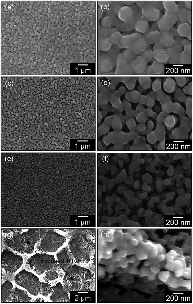 | ||
| Fig. 1 SEM images of films PVP0.05 (a and b), PVP0.10 (c and d), PVP0.25 (e and f) and PVP0.40 (g and h). | ||
The XRD patterns of films PVP0.05–0.40 are shown in Fig. 2. The diffraction patterns of the CuO (ICDD #00-005-0661) and FTO phases were detected for all the films. The residual carbon was evaluated by XPS analysis for films PVP0.05–0.40 (ESI Table S1†). A small amount of carbon below 2.5 atom% was detected in films PVP0.05–0.25. The carbon cannot originate from PVP but from the dust adsorbed on the films. No carbon was detected in film PVP0.40 even though the film was prepared from a solution with a larger amount of PVP. Fig. 3 shows the optical transmission spectra of films PVP0.05–0.40. Films PVP0.05–0.40 exhibited low transmittance at the wavelength of 300–800 nm, which could be attributed to the optical absorption by CuO (the band gap energy of CuO is 0.7–1.6 eV) and light scattering by the porous layer.
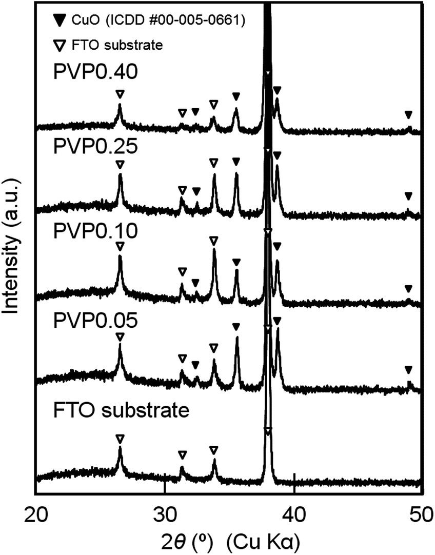 | ||
| Fig. 2 XRD patterns of the FTO substrate and films PVP0.05–0.40. | ||
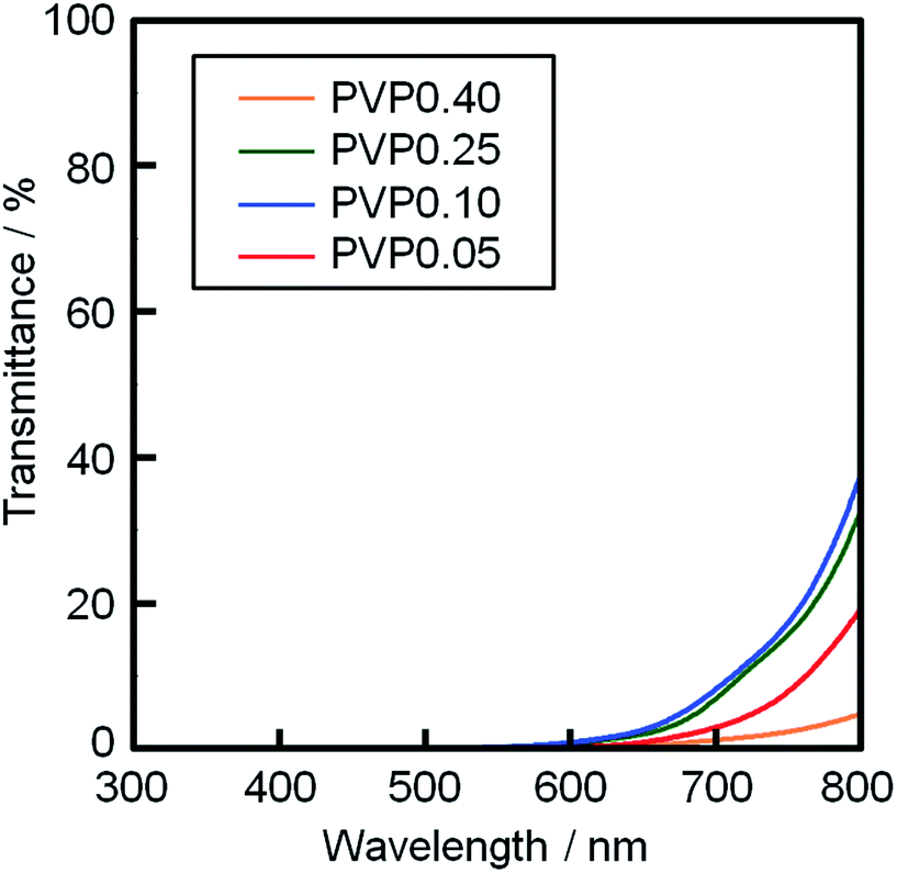 | ||
| Fig. 3 Optical transmission spectra of films PVP0.05–0.40. | ||
The photocathodic performance of films PVP0.05–0.40 was evaluated by measuring the current–potential curves and action spectra under irradiation of xenon light. The current–potential curves of films PVP0.05–0.40 are shown in Fig. 4. The curves were measured under the chopped white light, where the differences in the current measured in light and dark are regarded as the photocurrent. Negative photocurrent was detected at −0.5 to 0.1 V vs. SCE under the light irradiation for film PVP0.05–0.40 (Fig. 4), which means that all the CuO films worked as photocathode materials. A dark current was observed below −0.3 V vs. SCE (Fig. 4). Moreover, we examined the photoelectrochemical stability of films PVP0.05–0.40, where the current–potential curves of the films were measured for 30 min at a working electrode potential of −0.1 V vs. SCE under the white light. The photocurrent values reduced with light-irradiation time, which is attributed to photocorrosion of the CuO films.22,23 Films PVP0.05–0.40 exhibited a decrease of ca. 80% in the photocurrent after the irradiation of white light for 30 min irrespective of [PVP] (ESI Table S2†), which means that the porous structure of films PVP0.05–0.40 did not affect the photoelectrochemical stability.
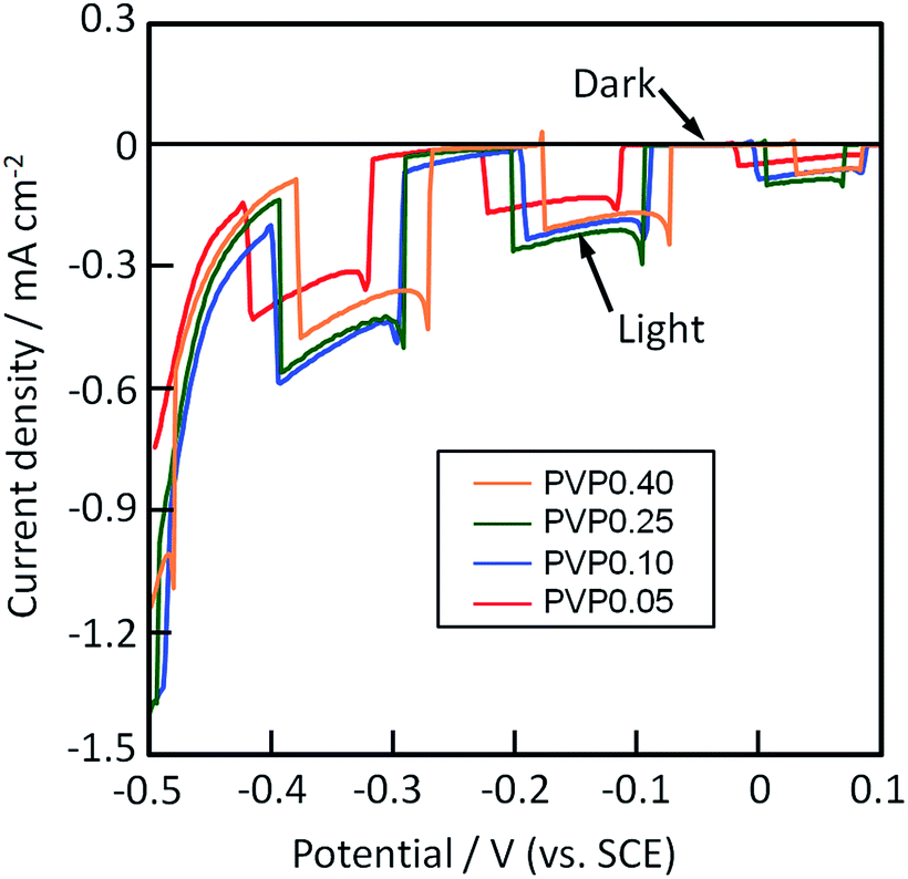 | ||
| Fig. 4 Current–potential curves measured under chopped white light for films PVP0.05–0.40. | ||
Fig. 5 shows the action spectra of films PVP0.05–0.40, which were measured at a working electrode potential of −0.1 V vs. SCE. For all the films, the photocurrent under the monochromatized light was detected at wavelengths between 300–800 nm, which agreed with the band gap energy of CuO (0.7–1.6 eV). The IPCE increased with increasing [PVP] from 0.05 to 0.25, where film PVP0.25 exhibited the maximum IPCE values of 8.7% and 3.9% at 300 and 500 nm, respectively. The highest photocathodic performance of film PVP0.25 could be attributed to the large surface area from the highly porous structure. The further increase in PVP content to [PVP] = 0.40 decreased IPCE, which could be caused by the partial delamination of the films due to the addition of a large amount of PVP.
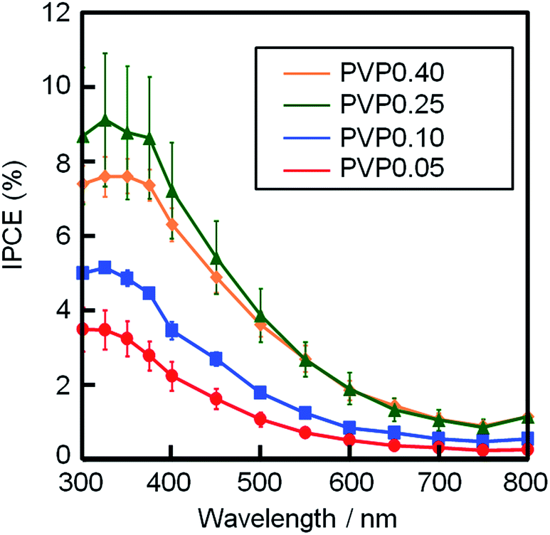 | ||
| Fig. 5 Action spectra of films PVP0.05–0.40. The measurement was conducted at −0.1 V vs. SCE. | ||
We also examined the effect of the film thickness on the photocathodic properties because the amount of CuO on the substrate might affect the photocathodic performance. As shown in Table 1, we obtained the CuO films with thickness below 200 nm and over 250 nm. We evaluated the IPCE values of all the samples, and investigated the influence of the amount of CuO on the photocathodic performance (the action spectra are shown in ESI Fig. S2†). As shown in Fig. S2,† the IPCE values increased with increasing film thickness up to ca. 200 nm, while a further increase in thickness over 200 nm did not lead to an increase in IPCE irrespective of [PVP]. Moreover, the variation in thickness did not provide a drastic change of the IPCE values compared with the porosity of the films (Fig. 5). These results also suggest that the difference in IPCE values among films PVP0.05–0.40, seen in Fig. 5, is mainly attributed to film porosity.
In the present study, the porous CuO film with thickness of ca. 230 nm (film PVP0.25) exhibited the maximum IPCE value, as shown in Fig. 5 and S2.† On the other hand, Saeid et al. reported the influence of film thickness on the photocathodic performance of sputter-deposited CuO film materials, where the CuO films with a thickness of ca. 550 nm showed the highest photocurrent among their CuO film products.23 Since their CuO films, which were obtained by the sputtering technique, had a highly dense structure consisting of nanocrystallites, such microstructure might provide the difference in the optimum thickness for the photoelectrochemical reaction with our porous CuO films.
Conclusions
Porous CuO films were obtained from Cu(NO3)2 aqueous solutions containing PVP ([PVP] = 0–0.50 M). PVP modified the wettability of FTO glass substrates and also created nanoscale pores in the resultant CuO films during heat treatment. The addition of PVP ([PVP] = 0.05–0.50 M) provided good wettability by the Cu(NO3)2 aqueous solutions, which enabled film formation on the substrates. The CuO films became porous as the PVP content increased ([PVP] = 0.05–0.25 M), while an excess amount of PVP ([PVP] > 0.40 M) led to film delamination during heat treatment. The CuO films showed a photocathodic response at wavelengths of 300–800 nm. The porous structure provided larger surface area that enhanced the photocathodic performance of the CuO films. Film PVP0.25 ([PVP] = 0.25 M) exhibited maximum IPCE values of 8.7% and 3.9% at wavelengths of 300 and 500 nm, respectively. The synthetic route with PVP can enable us to easily obtain porous metal oxide films with a good photoelectrode performance. The simple and convenient technique would be useful for the fabrication of functional film materials.References
- C. Y. Chiang, Y. Shin, K. Aroh and S. Ehrman, Int. J. Hydrogen Energy, 2012, 37, 8232–8239 CrossRef CAS.
- K. Nakaoka, J. Ueyama and K. Ogura, J. Electrochem. Soc., 2004, 151, C661–C665 CrossRef CAS.
- C. V. Niveditha, M. J. J. Fatima and S. Sindhu, J. Electrochem. Soc., 2016, 163, H426–H433 CrossRef CAS.
- X. H. Zhao, P. Wang, Z. X. Yan and N. F. Ren, Chem. Phys. Lett., 2014, 609, 59–64 CrossRef CAS.
- J. G. Lee, D. Y. Kim, J. H. Lee, M. W. Kim, S. An, H. S. Jo, C. Nervi, S. S. Al-Deyab, M. T. Swihart and S. S. Yoon, ACS Appl. Mater. Interfaces, 2016, 8, 15406–15414 CAS.
- Y. F. Lim, C. S. Chua, C. J. J. Lee and D. Z. Chi, Phys. Chem. Chem. Phys., 2014, 16, 25928–25934 RSC.
- S. Masudy-Panah, R. S. Moakhar, C. S. Chua, H. R. Tan, T. I. Wong, D. Z. Chi and G. K. Dalapati, ACS Appl. Mater. Interfaces, 2016, 8, 1206–1213 CAS.
- C. Liu, N. P. Dasgupta and P. D. Yang, Chem. Mater., 2014, 26, 415–422 CrossRef CAS.
- C. Wadia, A. P. Alivisatos and D. M. Kammen, Environ. Sci. Technol., 2009, 43, 2072–2077 CrossRef CAS PubMed.
- B. O'Regan and M. Grätzel, Nature, 1991, 353, 737–740 CrossRef.
- M. Grätzel, Nature, 2001, 414, 338–344 CrossRef PubMed.
- J. C. Yu, J. Yu, W. Ho, Z. Jiang and L. Zhang, Chem. Mater., 2002, 14, 3808–3816 CrossRef CAS.
- C. A. Grimes, J. Mater. Chem., 2007, 17, 1451–1457 RSC.
- H. Zhang, G. Chen and D. W. Bahnemann, J. Mater. Chem., 2009, 19, 5089–5121 RSC.
- D. S. Zhang, T. Yoshida and H. Minoura, Adv. Mater., 2003, 15, 814–817 CrossRef CAS.
- Z. F. Liu, Z. G. Jin, W. Li and J. J. Qiu, Mater. Lett., 2005, 59, 3620–3625 CrossRef CAS.
- J. G. Yu, X. J. Zhao and Q. N. Zhao, Thin Solid Films, 2000, 379, 7–14 CrossRef CAS.
- N. R. A. Manap and U. S. Jais, Mater. Res. Innovations, 2009, 13, 382–385 CrossRef CAS.
- G. Pia, L. Casnedi and U. Sanna, Ceram. Int., 2015, 41, 6350–6357 CrossRef CAS.
- K. H. Zuo, Y. A. Zhang, Y. P. Zeng and D. L. Jiang, Ceram. Int., 2011, 37, 407–410 CrossRef CAS.
- H. Kozuka and T. Kishimoto, Chem. Lett., 2001, 11, 1150–1151 CrossRef.
- A. Ray, I. Mukhopadhyay, R. Pati, Y. Hattori, U. Prakash, Y. Ishii and S. Kawasaki, J. Alloys Compd., 2017, 695, 3655–3665 CrossRef CAS.
- S. Masudy-Panah, R. S. Moakhar, C. S. Chua, A. Kushwaha, T. I. Wong and G. K. Dalapati, RSC Adv., 2016, 6, 29383–29390 RSC.
Footnote |
| † Electronic supplementary information (ESI) available. See DOI: 10.1039/c6ra26590a |
| This journal is © The Royal Society of Chemistry 2017 |