
 Open Access Article
 This Open Access Article is licensed under a
 Creative Commons Attribution 3.0 Unported Licence
Direct transfer of graphene and application in low-voltage hybrid transistors†
Huihui Zhu‡
ab,
Ao Liu‡c,
Fukai Shan*c,
Wenrong Yangd,
Colin Barrowd and
Jingquan Liu *ab
*ab
aCollege of Material Science and Engineering, Lab of New Fiber Materials and Modern Textile, Growing Base for State Key Laboratory, Qingdao University, Qingdao 266071, China. E-mail: jliu@qdu.edu.cn
bShandong Provincial Key Laboratory of Detection Technology for Tumor Markers, College of Chemistry and Chemical Engineering, Linyi University, Linyi 276005, China
cCollege of Electronic and Information Engineering, Lab of New Fiber Materials and Modern Textile, Growing Base for State Key Laboratory, Qingdao University, Qingdao 266071, China. E-mail: fukaishan@yahoo.com
dSchool of Life and Environmental Sciences, Deakin University, Geelong, VIC 3217, Australia
First published on 12th January 2017
Abstract
A novel scotch tape assisted direct transfer of graphene onto different flexible and rigid substrates, including paper, polyethylene terephthalate, flat and curved glass, SiO2/Si, and a solution-processed high-k dielectric layer is presented. This facile graphene transfer process is driven by the difference in adhesion energy of graphene with respect to tape and a target substrate. In addition, the graphene films transferred by scotch tape are found to be cleaner, more continuous, less doped and higher-quality than those transferred by PMMA. Based on that, the tape transferred graphene is employed as a carrier transport layer in oxide thin-film transistors (TFTs) with different gate dielectrics (i.e., SiO2 and high-k ZrO2). The In2O3/graphene/SiO2 TFTs exhibit a high electron mobility of 404 cm2 V−1 s−1 and a high on/off current ratio of 105, while the counterpart In2O3/graphene/ZrO2 TFTs exhibit improved electron transport properties at an ultra-low operating voltage of 3 V, which is 20 times lower than that of SiO2-based devices. In contrast, the ZrO2-based TFTs with PMMA-transferred graphene exhibit no detective electrical properties. Therefore, the proposed scotch tape assisted transfer method will be particularly useful for the production of graphene films and other two-dimensional materials in more cost-effective and environmentally friendly modes for broad practical applications beyond graphene-based field-effect transistors (GFETs).
Introduction
Graphene, consisting of single layered sp2 carbon atoms arranged in a honeycomb lattice, is a rapidly rising star on the horizon of materials science and has recently triggered intensive research activities worldwide due to its remarkable electrical, mechanical, and thermal properties.1–7 Among various preparation methods, chemical vapor deposition (CVD) has been identified as a relatively practical and reliable way to produce high-quality large-area graphene films on certain metal-foil subtrates.8–11 However, most electronic applications of CVD-graphene, e.g. touchscreens and organic light-emitting diodes, need an insulating substrate to support graphene films.12,13 As a result, a critical challenge has emerged: can we develop a reliable and practical method to transfer CVD-graphene from its growth substrate to the desired substrate without damaging the fragile patchwork or leaving unwanted residue on the graphene films?14Thus far, the commonly reported transfer techniques often involve the use of support layer like poly(methyl methacrylate) (PMMA).8,15–17 However, such wet transfer process is not suitable for the preparation of large-scale graphene films, as it requires handling skills to remove the polymer layer after transfer. It is also easy to leave some residue on graphene, which might cause inhomogeneous doping and degradation of charge carrier mobility.18–20 In addition, during the removal of polymer support layer, the sandwich structure of polymer/graphene/target, usually has to experience a long time organic solvent (e.g. acetone) bath or rinse, which significantly limits the free selection of target subtrates.21 Another approach is based on the elastomer stamp method,22–24 whereby graphene layer is released onto the target substrate by stamping. Although this method has built-in ‘pick-and-place’ capability, there is limitation on its applicability to certain flat, hard and hydrophilic surfaces. For dry transfer of CVD-graphene, thermal release tape (TRT) has been employed as a popular carrier foil, however, in this method, graphene sheet needs to be released by heating the tape. The high processing temperature is often close to the glass transition temperature (Tg) of polymer substrates, leading to considerable thermal stress on graphene.25 Recently, polymer-free transfer methods involving rigid frames have been reported by Zettl et al.26 and Cho et al.,27 however, these methods are not applicable to achieve large-scale transfer. Other transfer methods usually require high energy-consuming annealing or tedious wet cleaning processes, thus are also unfavorable for large-area graphene transfer.28,29
Owing to its extremely high charge carrier mobility, graphene has been attracting considerable interest for the fabrication of graphene-based field-effect transistors (GFETs). However, the GFETs generally exhibit poor current modulation ability with a low on/off current ratio (Ion/Ioff < 10),20,25,30,31 due to the semimetallic nature of graphene, particularly its gapless linear dispersion relation. On the contrary, the metal-oxide thin-film transistors (MOTFTs) usually exhibits high Ion/Ioff values (≥106).32–34 In our previous work, the TFTs based on bilayer oxides with a high conductive channel and a high resistant one can overcome the trade-off between high mobility and other parameters.35 In this regard, the hybrid TFTs based on bilayer graphene and oxide thin films are expected to exhibit high carrier mobility and keep the relatively high Ion/Ioff as well. The high operational voltage of GFETs based on SiO2 dielectric is another challenge because of the relatively low dielectric constant of SiO2 (k ∼ 3.9). To solve this problem, several approaches have been employed to achieve high capacitance of gate dielectrics by increasing the k value or decreasing the film thickness.36–38 For instance, the utilization of inorganic metal-oxide high-k dielectrics, such as HfO2, Al2O3, and ZrO2, could achieve a low leakage current, through the use of a thicker film, as well as a low-voltage operation.
In this work, we introduced the scotch tape assisted direct transfer of CVD-graphene onto both flexible and rigid substrates at room temperature. This easy and new transfer method can offer researchers much freedom to choose target substrates, for the direct pasting and peeling processes of scotch tape substitute the tedious coating and dissolving processes of polymer layer. The scotch tape transferred graphene films are cleaner, more continuous, less doped and higher-quality than those transferred by PMMA, as evidenced by scanning electron microscope (SEM) and atomic force microscope (AFM) images, Raman spectra, and electrical characterizations. Furthermore, we investigated the performance of hybrid TFTs with scotch tape transferred graphene and In2O3 bilayer channels on different gate dielectrics (i.e., SiO2 and high-k ZrO2). The hybrid In2O3/graphene/SiO2 TFTs exhibited higher carrier mobility and Ion/Ioff than the pristine In2O3 ones. Notably, by replacing SiO2 with ZrO2, the resulting transistors exhibited an ultra-low operating voltage of 3 V, which is 20 times lower than that of SiO2-based devices.
Experimental
Graphene transfer
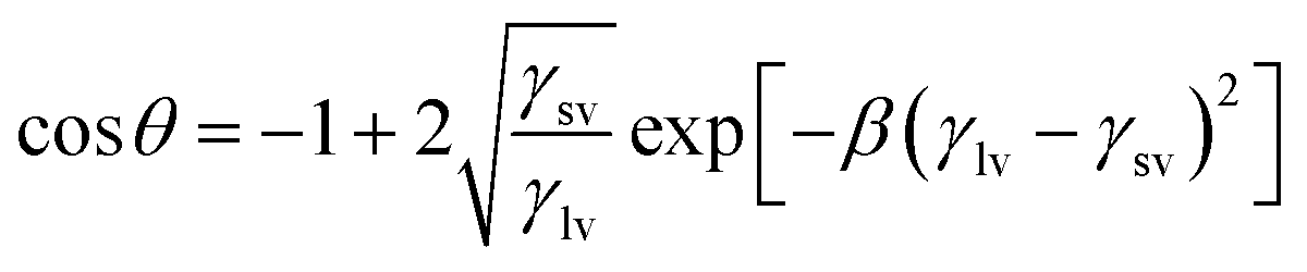
Graphene was grown on Cu foils using the method as reported by Li et al.8 The backside graphene was removed by exposing it to oxygen plasma for 10 min. Then, scotch tape (Scotch, 810#) was laminated onto the graphene/Cu. Cu was further etched by 1 M FeCl3 solution in etchant box, and the tape/graphene was rinsed with ultrapure water prior to transfer. The target substrates were exposed to the oxygen plasma for dry cleaning and strong adhesion to the graphene film. The tape/graphene layer was attached to the substrate, and stored in dehydrated condition for 5 h. After peeling off the tape, graphene was transferred onto target substrates. The contrastive PMMA transfer was conducted following these steps: (1) spin-coating PMMA layer on one side of graphene/Cu; (2) floating the layer structure on etchant to remove the Cu foil; (3) transferring the PMMA/graphene to the target substrates, and then removing PMMA by acetone bath for 48 h.The calculation of surface energy from contact angle:
 | (1) |
γlv![[thin space (1/6-em)]](https://www.rsc.org/images/entities/char_2009.gif) cosθ = γsv − γsl, (Young equation) cosθ = γsv − γsl, (Young equation)
| (2) |
The surface energy is calculated from modified Berthelot rule (eqn (1)) and Young's equation:
 | (3) |
TFT fabrication
The preparation details for solution-processed In2O3 and ZrO2 precursor solutions can be found in our previous works.34,35,39 For the In2O3/SiO2 TFT, the as-prepared In2O3 precursor solution was spin-coated on the thermally grown SiO2 dielectric at 3500 rpm for 15 s. The coated film was annealed at 120 °C for 2 h in air and subsequently annealed in a rapid thermal annealing system at 150 °C for 1 h, under a vacuum of 5 × 10⁻² atm. For the fabrication of In2O3/graphene hybrid TFTs, the In2O3 precursor solution was separately spin-coated on the graphene attached SiO2 and ZrO2 substrates and followed by the same thermal treatments as above. Finally, the Al source and drain electrodes were evaporated on the In2O3 channel layer through a shadow mask. The channel length and width of the transistors are 100 and 1000 μm, respectively. The filed-effect mobility (μFE) was extracted from the transfer curves using the following equation:40
 | (4) |
Characterizations
The water contact angles were measured by a drop shape analyzer, DSA100. SEM images were acquired on a JEOL JSM-6700F scanning electron microscope. AFM images were taken using a Veeco D3100 atomic force microscope. The TEM images were taken on a JEM-2100 transmission electron microscope with the graphene samples transferred onto a lacey carbon copper TEM grid. Raman spectra were obtained using a RENISHAW RM2000 Raman System and Raman excitation wavelength is 532 nm. The sheet resistance of the graphene was measured using a four-point probe with a nanovoltmeter (Keithley 6221, 2182A). The transparency of graphene on glass was investigated by using a UV-vis-NIR spectrophotometer (Hewlett-Packard). The electrical characteristics of the devices were measured using a semiconductor parameter analyzer (Keithley 2634B) in the dark box.Results and discussion
Fig. 1 illustrates the schematic diagram of scotch tape assisted direct transfer process of as-grown CVD-graphene on Cu foil to arbitrary substrates. The preliminary steps involving graphene growth and attaching graphene/Cu to scotch tape, and the detailed etching process of Cu layers are described in the Experimental section. Scotch tape was first attached to CVD-graphene/Cu foil as shown in Fig. 1a. After completely removing Cu by etching, the graphene on the supporting tape was rinsed with ultrapure water and transferred onto target substrate. Finally, the tape was peeled off, leaving graphene on the target substrate (corresponding photographs can be seen in Fig. S1†). Panels b to e of Fig. 1 show the graphene films transferred onto scotch tape, SiO2/Si, glass and PET, respectively.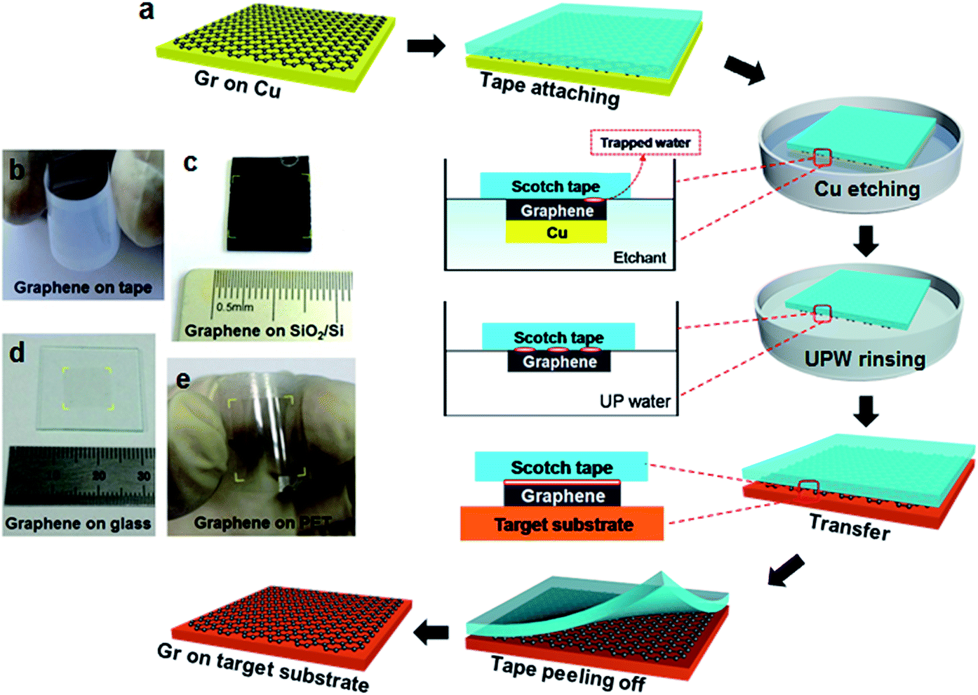 | ||
| Fig. 1 (a) Schematic representation of transferring graphene from copper foil to target substrates. Photographs of graphene films transferred onto (b) scotch tape, (c) SiO2/Si, (d) glass and (e) PET. (Gr refers to graphene.) | ||
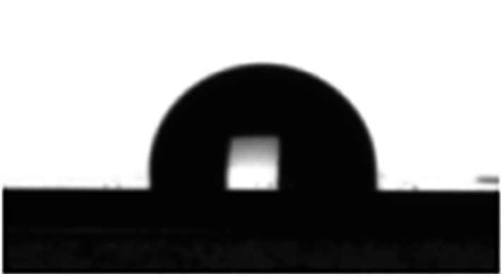
It is noted that during the process of Cu etching, water molecules diffused into the interface between the scotch tape and graphene. This significantly weakened the adhesive force of the tape because of the saturation of hydrogen bonds on the tape, and the increase of the intermolecular distance between tape and graphene, which consequently results in the decrease of van der Waals force. In addition, the graphene transfer onto glass or SiO2 substrates tends to be easier due to the stronger charge-transfer interaction between graphene and oxygen-rich surface.41,42 Therefore, the scotch tape assisted direct transfer is driven by the difference in adhesion energy of graphene with respect to scotch tape and a target substrate, which was exposed to oxygen plasma prior to use (see Fig. S2, ESI† for more details about the transfer mechanism). Furthermore, in order to compare the surface energies of various substrates with or without graphene, the contact angles of water droplets on SiO2/Si, scotch tape, graphene on SiO2/Si, and graphene on scotch tape were measured. As shown in Table 1, the SiO2/Si surface exhibits the smallest contact angle, i.e., the largest surface energy. Thus, the graphene that was weakly adherent to scotch tape can be easily transferred to SiO2/Si substrates as a result of the large difference in their surface energies (65.61 vs. 26.30 dyn per cm).22
| SiO2/Si | G/SiO2/Si | S-Tape | G/S-Tape | |
|---|---|---|---|---|
| γ (dyn per cm) | 65.61 | 37.80 | 26.30 | 30.35 |
| θ (°) | 27.47 | 76.24 | 94.66 | 88.15 |
| Optical image |  |
 |
 |
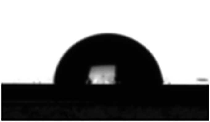 |
Fig. 2 presents the various characterizations via SEM, AFM and secondary electron imaging, which confirm that unbroken graphene monolayers can be successfully transferred using scotch tape assisted transfer method. SEM (Fig. 2a) and secondary electron images (Fig. 2b) of CVD-graphene on copper foil clearly show that the as-grown graphene is continuous with periodic steps, which result from the Cu surface reconstruction and the surface faceting evolution during the cooling process.43 For comparison, the morphological images of the CVD-graphene transferred with the assistance of both scotch tape and PMMA were carefully analyzed by SEM and AFM. As shown in Fig. 2c and d, the scotch tape transferred graphene film is clean, and shows a relatively uniform morphology with no significant macroscopic defects, while its counterpart, PMMA transferred graphene film, shows undesired residue and wrinkles. Similarly, the AFM data also demonstrate the uniformity and cleanliness of graphene films transferred by scotch tape (Fig. 2e), and the micron-sized cracks and defects on the ones transferred by PMMA (Fig. 2f). The thickness of monolayer graphene transferred by scotch tape is ∼1 nm (corresponding TEM image and selected area electron diffraction (SAED) pattern can be seen in Fig. S3†), which is slightly smaller than that of graphene transferred by PMMA (∼1.2 nm), suggesting the better conformal contact between the scotch tape transferred graphene and the substrate.25
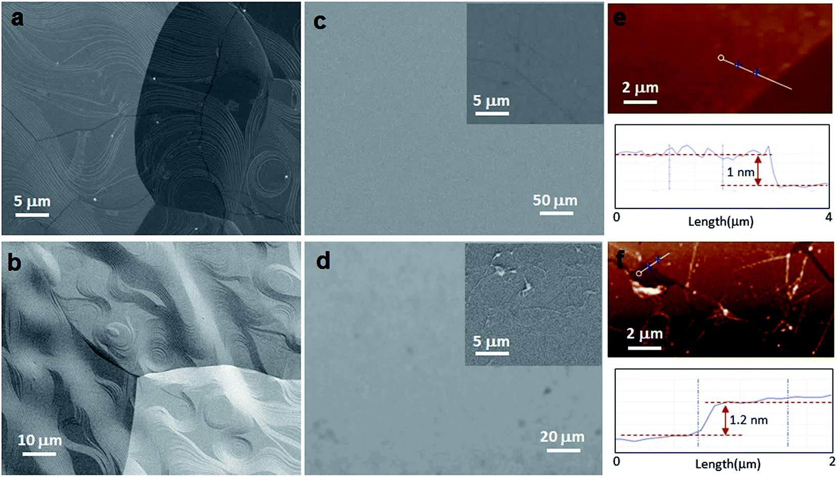 | ||
| Fig. 2 (a) SEM and (b) secondary electron images of CVD-graphene on copper foil, showing the continuity and periodic steps of graphene. (c, d) SEM images at low and high (insets) magnifications of graphene transferred by scotch tape and PMMA, respectively. (e) AFM image of graphene transferred by scotch tape method showing a clean graphene film with a thickness of ∼1 nm. (f) AFM image of graphene transferred by PMMA method showing graphene film with some defects and a thickness of 1.2 nm. | ||
The quality of scotch tape transferred graphene film on SiO2/Si was further investigated by Raman spectroscopy, which is an unambiguous method to evaluate the quality and the number of graphene layers.44 Fig. 3a shows a single Raman spectrum with characteristic peaks of graphene G-band centered at ∼1581.9 cm−1, and 2D-band at ∼2652.6 cm−1, without visible D-band. The narrow and symmetric Lorentzian 2D peak shows a full width at half-maximum (FWHM) of only ∼23.31 cm−1. The D-, G- and 2D-band Raman maps as shown in Fig. 3b–d, respectively, confirm that the transferred monolayer graphene is high-quality and continuous. In addition, the intensity ratio of D-band to G-band is less than 0.1 across the film (Fig. 3e), while the intensity ratio of 2D-band to G-band is more than 2 (Fig. 3f). The above results again suggest the scotch tape transferred graphene is monolayered and continuous with high quality.
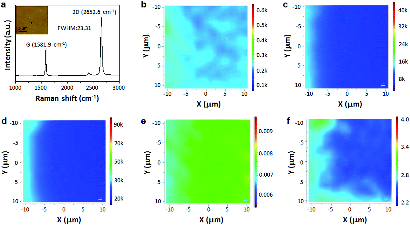 | ||
| Fig. 3 (a) A single Raman spectrum and Raman maps for graphene transferred onto SiO2/Si by scotch tape: (b) D-band (∼1335 cm−1), (c) G-band (∼1582 cm−1), (d) 2D-band (∼2653 cm−1), (e) D-band to G-band intensity ratio, and (f) 2D-band to G-band intensity ratio. The inset shows the corresponding optical microscope image. | ||
The Raman spectrum of PMMA transferred graphene on SiO2/Si shows the obvious D-band (∼1338.2 cm−1), G-band (∼1588.7 cm−1), and 2D-band (∼2698.9 cm−1) with a relatively high FWHM of 41.72 cm−1 (Fig. S4†). It is noteworthy that the G and 2D band peaks of graphene transferred using PMMA are obviously blue-shifted compared to that transferred using scotch tape (Fig. S5†), indicating that the scotch tape transferred graphene is almost free from polymer residues that results in p-doping.45
The electrical property of scotch tape transferred graphene is tested by the four-probe measurement of sheet resistance. As shown in Fig. 4a, the resistance distribution of the graphene transferred onto glass by scotch tape is found to be in a range from 483 to 621 Ω □−1. Fig. 4b compares the statistics of the sheet resistance. The average values were ∼550, ∼510 and ∼600 Ω □−1 for graphene transferred on SiO2/Si, PET and glass substrates transferred by scotch tape. By contrast, the average values were ∼1300, ∼1380 and ∼1610 Ω □−1 for the respective counterpart transferred by PMMA. The sheet resistances of scotch tape transferred graphene are less than half of the values for that transferred by PMMA. This improvement can be attributed to the continuity and higher quality of the scotch tape transferred graphene. The transmittance data as a function of wavelength for 1–4 layered graphene films transferred onto glass by scotch tape and the corresponding sample photographs are shown in Fig. 4c. Fig. 4d gives the transmittance at λ = 550 nm as a function of the layer number of the graphene films. The attenuation coefficient was found to be 2.5% per layer by fitting the data to Beer's law. This value is very close to the theoretical value of 2.3%.46,47 One key success of our scotch tape transfer method is the capability to achieving continuous graphene films, whose sheet resistance could reach as low as ∼145 Ω □−1 (at 89.9% transparency) and optical transparency as high as 97.5% (with Rsheet ≈ 600 Ω □−1).
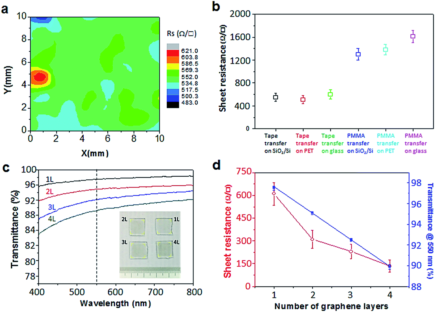 | ||
| Fig. 4 (a) The spatial distribution of sheet resistances for graphene transferred onto SiO2/Si by scotch tape. (b) Comparison of sheet resistance of graphene transferred onto SiO2/Si, PET and glass by scotch tape and PMMA, respectively. (c) Transmittance of n-layer graphene films transferred onto glass by scotch tape. Inset is photograph of graphene films with different stacked graphene layers on glass. (d) Sheet resistance and transmittance of graphene films as a function of the number of stacked graphene layers transferred onto glass by scotch tape. | ||
Photographs of graphene transferred by scotch tape are shown in Fig. 5. A light-emitting diode (LED) could be turned on when the graphene on tape was connected in the circuit (Fig. 5a), suggesting that the graphene is electrically continuous. As a control, when the bare scotch tape was connected, LED kept off (Fig. S6†). Fig. 5b–d show that the scotch tape assisted transfer method is applicable to not only typical rigid substrates like glass, but also some flexible whiteboard paper (Fig. 5c) and curved bottle surface (Fig. 5d), which are quite advantageous over most other reported transfer methods.16,18,31,48
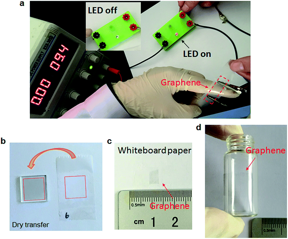 | ||
| Fig. 5 (a) Demonstration of a light-emitting diode (LED) connected through the graphene sheet. Operating voltage, 9.4 V. Inset is the off state of LED. Photograph of graphene transfer on glass (b), on whiteboard paper (c), and on curved surface (d). | ||
Based on the superior optical and electrical properties of scotch tape transferred graphene films, their applications in thin-film transistors (TFTs) were further explored. It is well-known that the transportation of free carrier in TFTs is limited in a narrow region of the interface between channel and dielectric layers.35 Therefore, the interface modification is critical to achieve high-performance transistors. In our previous work, the ultra-thin highly conductive In2O3 thin film was inserted as the carrier transport layer to achieve a 5 times larger mobility compared with single-layer oxide TFT. In this work, the scotch tape transferred graphene film was adopted as a better candidate because of the low defect states and high conductivity.
The schematic of pristine In2O3 TFT with a bottom-gate and top-contact structure is shown in Fig. 6a. The corresponding transfer curve of the as-prepared In2O3 TFT at a drain voltage (VDS) of 60 V is presented in Fig. 6b. The device exhibits a typical unipolar n-channel transistor behavior with an Ion/Ioff of 106 and an electron mobility (μe) of 1.21 cm2 V−1 s−1. Interestingly, by inserting scotch tape transferred graphene film between In2O3 and SiO2 layers (Fig. 6c), the In2O3/graphene hybrid TFTs showed an ambipolar behavior due to the ambipolar nature of graphene thin film.49 Therefore, the device exhibited both electron- and hole-induced current in positive and negative bias voltage region. As shown in Fig. 6d, the as-prepared In2O3/graphene hybrid TFT exhibited significantly increased μe of 404 ± 18 cm2 V−1 s−1 and large Ion/Ioff of 105. To date, several approaches have been adopted to achieve high-mobility oxide TFTs, such as Li-doped ZnO (μe = 54 cm2 V−1 s−1) TFT,50 single-walled carbon nanotube (SWNT)-doped InZnO (μe = 140 cm2 V−1 s−1) TFT,51 silver nanowire (AgNW)-doped InGaZnO (μe = 174 cm2 V−1 s−1) TFT,52 and ZnO/graphene transferred by PMMA (μe = 329.7 ± 16.9 cm2 V−1 s−1) TFT.53 Although the higher mobility was obtained in common CVD-graphene based devices, the poor current modulation (Ion/Ioff < 10) was observed simultaneously.36,37,54,55 The small Ion/Ioff value is mainly caused by the large off-state current (Ioff), which could lead to inevitable static power consumption. It is known that static power consumption is comparable to dynamic power in modern silicon chips or even become dominating in the future.56 Therefore, the low Ioff has been regarded as a critical parameter to evaluate the power consumption of a device in modern integrated circuits. Generally, for the practical application in analog circuits, an Ion/Ioff of larger than 104 is desirable.57
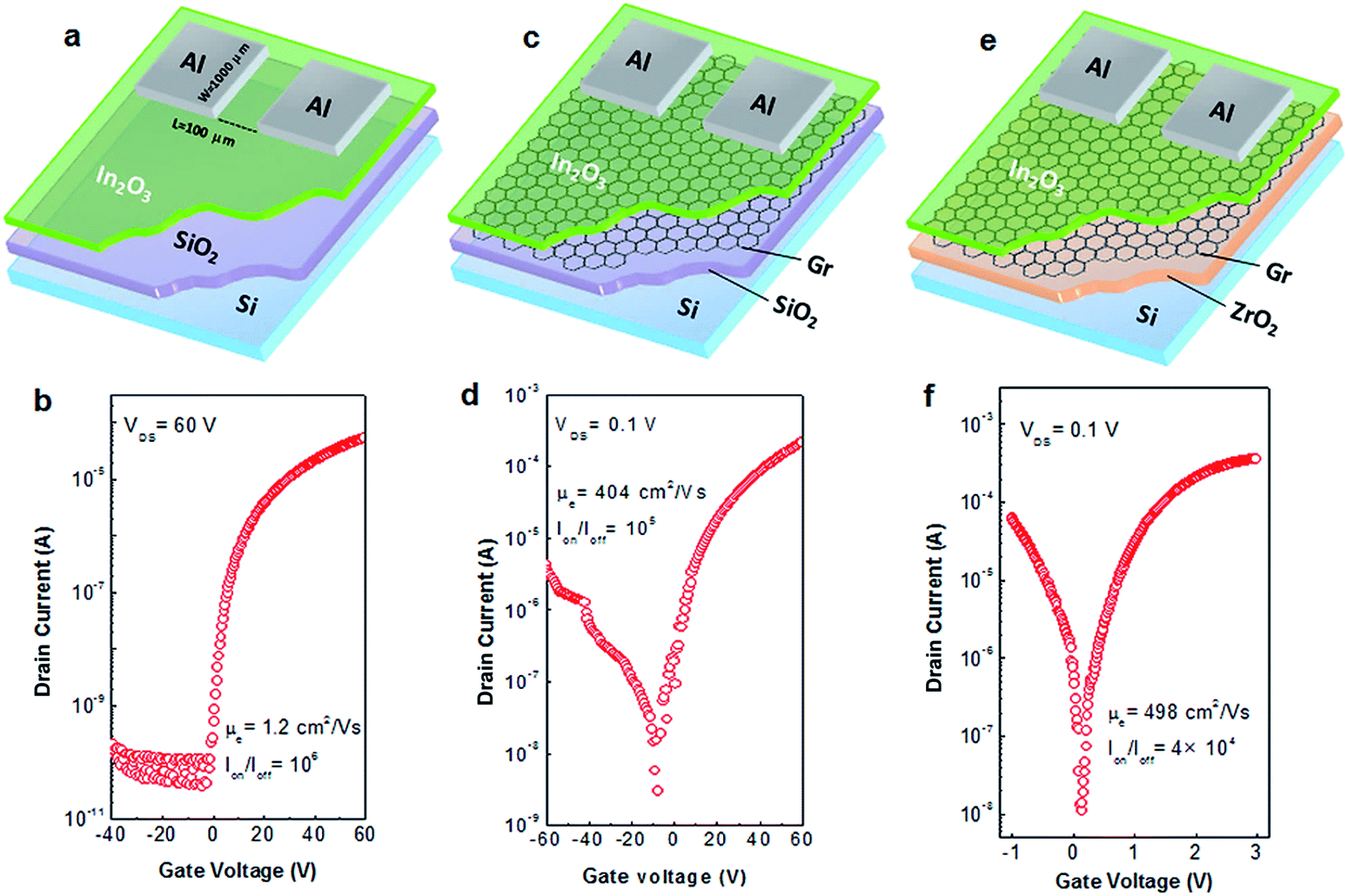 | ||
| Fig. 6 Schematic illustration of the fabrication of different TFTs and the corresponding transfer characteristics. (a, b) pristine In2O3 TFT, (c, d) In2O3/graphene TFT, and (e, f) In2O3/graphene TFT on high-k ZrO2. | ||
In addition, it can be seen that all these high-mobility oxide TFTs operated at high voltages ranging from 20 V to 100 V, which originates from the small dielectric constant and thick film thickness of SiO2 dielectric. The large operating voltage results in high power consumption, thus significantly hinders their applications in portable equipment, such as smart phones and tablet personal computers, due to the limited capacity of rechargeable battery. In our previous works,32,33,58 various inorganic high-k dielectrics were synthesized via solution route and applied as gate dielectric in TFTs. Compared with conventional SiO2-based TFTs, the resulting ones exhibited improved electrical performance at much lower operating voltages. Herein, the high-k ZrO2 was employed as gate dielectric instead of SiO2. The electrical performance of ZrO2 dielectric layer is shown in Fig. S7.† The In2O3/graphene hybrid TFTs on ZrO2 represented improved carrier transport properties with an enhanced μe of 498 ± 20 cm2 V−1 s−1 (Fig. 6e and f). In particular, the fabricated transistors could be operated at an ultra-low voltage of 3 V, which is 20 times lower than that of SiO2-based In2O3/graphene hybrid TFTs. For comparison, the ZrO2-based TFTs with graphene film transferred by PMMA were also fabricated and their performances examined. However, it was found that these hybrid TFTs exhibited no detective electrical properties, which should be attributed to the destruction of the ZrO2 dielectric by the acetone bath applied during PMMA removing process, as evidenced by the AFM analysis (Fig. S8†).
Conclusions
In summary, we have presented the scotch tape assisted direct transfer of CVD-graphene onto various flexible and rigid substrates at room temperature. This new method is simple, cost-effective and easily scalable, and can yield cleaner, more continuous, less doped and higher-quality graphene, as compared with the popular PMMA transfer method. By incorporating the transferred graphene films as carrier transport layer in oxide TFTs, the as-fabricated In2O3/graphene hybrid TFT represented a high μe of 404 cm2 V−1 s−1 and a high Ion/Ioff ratio of 105. Furthermore, this new method enabled us to fabricate the In2O3/graphene hybrid TFTs on solution-processed high-k ZrO2 gate dielectric. These TFTs exhibited improved carrier transport properties at an extremely low operating voltage of 3 V, which is 20 times lower than that of SiO2-based devices. Therefore, it is envisioned that the proposed scotch tape assisted transfer method would be particularly useful for more cost-effective and environmentally friendly production of graphene films or other two-dimensional materials such as boron nitride, and also pave the way for the development of diverse applications that span beyond GFETs.Acknowledgements
This work was supported by Qingdao Innovation Leading Talent Program and Natural Science Foundation of Qingdao (12-1-4-2-2-jch) and Natural Science Foundation of China (Grant No. 51472130 and 51572135).Notes and references
- K. S. Novoselov, A. K. Geim, S. Morozov, D. Jiang, Y. Zhang, S. Dubonos, I. Grigorieva and A. Firsov, Science, 2004, 306, 666–669 CrossRef CAS PubMed.
- A. K. Geim and K. S. Novoselov, Nat. Mater., 2007, 6, 183–191 CrossRef CAS PubMed.
- M. J. Allen, V. C. Tung and R. B. Kaner, Chem. Rev., 2009, 110, 132–145 CrossRef PubMed.
- C. N. R. Rao, A. K. Sood, K. S. Subrahmanyam and A. Govindaraj, Angew. Chem., Int. Ed., 2009, 48, 7752–7777 CrossRef CAS PubMed.
- A. K. Geim, Science, 2009, 324, 1530–1534 CrossRef CAS PubMed.
- F. Bonaccorso, Z. Sun, T. Hasan and A. Ferrari, Nat. Photonics, 2010, 4, 611–622 CrossRef CAS.
- N. O. Weiss, H. Zhou, L. Liao, Y. Liu, S. Jiang, Y. Huang and X. Duan, Adv. Mater., 2012, 24, 5782–5825 CrossRef CAS PubMed.
- X. Li, W. Cai, J. An, S. Kim, J. Nah, D. Yang, R. Piner, A. Velamakanni, I. Jung and E. Tutuc, Science, 2009, 324, 1312–1314 CrossRef CAS PubMed.
- S. J. Chae, F. Güneş, K. K. Kim, E. S. Kim, G. H. Han, S. M. Kim, H. J. Shin, S. M. Yoon, J. Y. Choi and M. H. Park, Adv. Mater., 2009, 21, 2328–2333 CrossRef CAS.
- X. Li, C. W. Magnuson, A. Venugopal, R. M. Tromp, J. B. Hannon, E. M. Vogel, L. Colombo and R. S. Ruoff, J. Am. Chem. Soc., 2011, 133, 2816–2819 CrossRef CAS PubMed.
- C. Mattevi, H. Kim and M. Chhowalla, J. Mater. Chem., 2011, 21, 3324–3334 RSC.
- S. Bae, H. Kim, Y. Lee, X. Xu, J.-S. Park, Y. Zheng, J. Balakrishnan, T. Lei, H. R. Kim and Y. I. Song, Nat. Nanotechnol., 2010, 5, 574–578 CrossRef CAS PubMed.
- N. Li, S. Oida, G. S. Tulevski, S.-J. Han, J. B. Hannon, D. K. Sadana and T.-C. Chen, Nat. Commun., 2013, 4, 2294 Search PubMed.
- J. Song, F.-Y. Kam, R.-Q. Png, W.-L. Seah, J.-M. Zhuo, G.-K. Lim, P. K. Ho and L.-L. Chua, Nat. Nanotechnol., 2013, 8, 356–362 CrossRef CAS PubMed.
- L. Gomez De Arco, Y. Zhang, C. W. Schlenker, K. Ryu, M. E. Thompson and C. Zhou, ACS Nano, 2010, 4, 2865–2873 CrossRef CAS PubMed.
- X. Li, Y. Zhu, W. Cai, M. Borysiak, B. Han, D. Chen, R. D. Piner, L. Colombo and R. S. Ruoff, Nano Lett., 2009, 9, 4359–4363 CrossRef CAS PubMed.
- L. Gao, W. Ren, H. Xu, L. Jin, Z. Wang, T. Ma, L.-P. Ma, Z. Zhang, Q. Fu and L.-M. Peng, Nat. Commun., 2012, 3, 699 CrossRef PubMed.
- J. Kang, S. Hwang, J. H. Kim, M. H. Kim, J. Ryu, S. J. Seo, B. H. Hong, M. K. Kim and J.-B. Choi, ACS Nano, 2012, 6, 5360–5365 CrossRef CAS PubMed.
- X. Liang, Z. Fu and S. Y. Chou, Nano Lett., 2007, 7, 3840–3844 CrossRef CAS.
- X.-D. Chen, Z.-B. Liu, C.-Y. Zheng, F. Xing, X.-Q. Yan, Y. Chen and J.-G. Tian, Carbon, 2013, 56, 271–278 CrossRef CAS.
- J. Kang, D. Shin, S. Bae and B. H. Hong, Nanoscale, 2012, 4, 5527–5537 RSC.
- S. J. Kang, B. Kim, K. S. Kim, Y. Zhao, Z. Chen, G. H. Lee, J. Hone, P. Kim and C. Nuckolls, Adv. Mater., 2011, 23, 3531–3535 CrossRef CAS PubMed.
- X. Li, W. Cai, I. H. Jung, J. H. An, D. Yang, A. Velamakanni, R. Piner, L. Colombo and R. S. Ruoff, ECS Trans., 2009, 19, 41–52 CAS.
- Y. Lee, S. Bae, H. Jang, S. Jang, S.-E. Zhu, S. H. Sim, Y. I. Song, B. H. Hong and J.-H. Ahn, Nano Lett., 2010, 10, 490–493 CrossRef CAS PubMed.
- S. J. Kim, T. Choi, B. Lee, S. Lee, K. Choi, J. B. Park, J. M. Yoo, Y. S. Choi, J. Ryu and P. Kim, Nano Lett., 2015, 15, 3236–3240 CrossRef CAS PubMed.
- W. Regan, N. Alem, B. Alemán, B. Geng, Ç. Girit, L. Maserati, F. Wang, M. Crommie and A. Zettl, Appl. Phys. Lett., 2010, 96, 113102 CrossRef.
- T. Yoon, W. C. Shin, T. Y. Kim, J. H. Mun, T.-S. Kim and B. J. Cho, Nano Lett., 2012, 12, 1448–1452 CrossRef CAS PubMed.
- Y.-C. Lin, C. Jin, J.-C. Lee, S.-F. Jen, K. Suenaga and P.-W. Chiu, ACS Nano, 2011, 5, 2362–2368 CrossRef CAS PubMed.
- X. Liang, B. A. Sperling, I. Calizo, G. Cheng, C. A. Hacker, Q. Zhang, Y. Obeng, K. Yan, H. Peng and Q. Li, ACS Nano, 2011, 5, 9144–9153 CrossRef PubMed.
- B. Wang, M. Huang, L. Tao, S. H. Lee, A.-R. Jang, B.-W. Li, H. S. Shin, D. Akinwande and R. S. Ruoff, ACS Nano, 2016, 10, 1404–1410 CrossRef CAS PubMed.
- D. Zhang, Z. Jin, J. Shi, X. Wang, S. Peng and S. Wang, Chem. Commun., 2015, 51, 2987–2990 RSC.
- G. Liu, A. Liu, H. Zhu, B. Shin, E. Fortunato, R. Martins, Y. Wang and F. Shan, Adv. Funct. Mater., 2015, 25, 2564–2572 CrossRef CAS.
- A. Liu, G. Liu, H. Zhu, H. Song, B. Shin, E. Fortunato, R. Martins and F. Shan, Adv. Funct. Mater., 2015, 25, 7180–7188 CrossRef CAS.
- A. Liu, G. X. Liu, H. H. Zhu, F. Xu, E. Fortunato, R. Martins and F. K. Shan, ACS Appl. Mater. Interfaces, 2014, 6, 17364–17369 CAS.
- G. Liu, A. Liu, F. Shan, Y. Meng, B. Shin, E. Fortunato and R. Martins, Appl. Phys. Lett., 2014, 105, 113509 CrossRef.
- J. Zhu, J. Kang, J. Kang, D. Jariwala, J. D. Wood, J.-W. T. Seo, K.-S. Chen, T. J. Marks and M. C. Hersam, Nano Lett., 2015, 15, 7029–7036 CrossRef PubMed.
- H. N. Arnold, C. D. Cress, J. J. McMorrow, S. W. Schmucker, V. K. Sangwan, L. Jaber-Ansari, R. Kumar, K. P. Puntambekar, K. A. Luck and T. J. Marks, ACS Appl. Mater. Interfaces, 2016, 8, 5058–5064 CAS.
- S.-J. Jeong, Y. Gu, J. Heo, J. Yang, C.-S. Lee, M.-H. Lee, Y. Lee, H. Kim, S. Park and S. Hwang, Sci. Rep., 2016, 6, 20907 CrossRef CAS PubMed.
- G. Liu, A. Liu, Y. Meng, F. Shan, B. Shin, W. Lee and C. Cho, J. Nanosci. Nanotechnol., 2015, 15, 2185–2191 CrossRef CAS PubMed.
- E. Fortunato, P. Barquinha and R. Martins, Adv. Mater., 2012, 24, 2945–2986 CrossRef CAS PubMed.
- X. Fan, W. Zheng, V. Chihaia, Z. Shen and J.-L. Kuo, J. Phys.: Condens. Matter, 2012, 24, 305004 CrossRef CAS PubMed.
- A. Rudenko, F. Keil, M. Katsnelson and A. Lichtenstein, Phys. Rev. B: Condens. Matter Mater. Phys., 2011, 84, 085438 CrossRef.
- Z.-J. Wang, G. Weinberg, Q. Zhang, T. Lunkenbein, A. Klein-Hoffmann, M. Kurnatowska, M. Plodinec, Q. Li, L. Chi and R. Schloegl, ACS Nano, 2015, 9, 1506–1519 CrossRef CAS PubMed.
- M. S. Dresselhaus, A. Jorio, M. Hofmann, G. Dresselhaus and R. Saito, Nano Lett., 2010, 10, 751–758 CrossRef CAS PubMed.
- A. Ferrari, J. Meyer, V. Scardaci, C. Casiraghi, M. Lazzeri, F. Mauri, S. Piscanec, D. Jiang, K. Novoselov and S. Roth, Phys. Rev. Lett., 2006, 97, 187401 CrossRef CAS PubMed.
- R. Nair, P. Blake, A. Grigorenko, K. Novoselov, T. Booth, T. Stauber, N. Peres and A. Geim, Science, 2008, 320, 1308 CrossRef CAS PubMed.
- P. Blake, P. D. Brimicombe, R. R. Nair, T. J. Booth, D. Jiang, F. Schedin, L. A. Ponomarenko, S. V. Morozov, H. F. Gleeson and E. W. Hill, Nano Lett., 2008, 8, 1704–1708 CrossRef PubMed.
- L. G. Martins, Y. Song, T. Zeng, M. S. Dresselhaus, J. Kong and P. T. Araujo, Proc. Natl. Acad. Sci. U. S. A., Early Ed., 2013, 110, 17762–17767 CrossRef CAS PubMed.
- K. S. Novoselov, A. K. Geim, S. Morozov, D. Jiang, Y. Zhang, S. a. Dubonos, I. Grigorieva and A. Firsov, Science, 2004, 306, 666–669 CrossRef CAS PubMed.
- G. Adamopoulos, A. Bashir, S. Thomas, W. P. Gillin, S. Georgakopoulos, M. Shkunov, M. A. Baklar, N. Stingelin, R. C. Maher and L. F. Cohen, Adv. Mater., 2010, 22, 4764–4769 CrossRef CAS PubMed.
- X. Liu, C. Wang, B. Cai, X. Xiao, S. Guo, Z. Fan, J. Li, X. Duan and L. Liao, Nano Lett., 2012, 12, 3596–3601 CrossRef CAS PubMed.
- H.-C. Liu, Y.-C. Lai, C.-C. Lai, B.-S. Wu, H.-W. Zan, P. Yu, Y.-L. Chueh and C.-C. Tsai, ACS Appl. Mater. Interfaces, 2014, 7, 232–240 Search PubMed.
- W. Song, S. Y. Kwon, S. Myung, M. W. Jung, S. J. Kim, B. K. Min, M.-A. Kang, S. H. Kim, J. Lim and K.-S. An, Sci. Rep., 2014, 4, 4064 Search PubMed.
- S. Zhou, Y. Su, Y. Xiao, N. Zhao, J. Xu and C. Wong, Nanotechnology, 2014, 25, 265201 CrossRef PubMed.
- S. K. Ameri, P. K. Singh, A. J. D'Angelo, M. J. Panzer and S. R. Sonkusale, Adv. Electron. Mater., 2016, 2, 1500355 CrossRef.
- M. L. Geier, P. L. Prabhumirashi, J. J. Mcmorrow, W. Xu, J. W. T. Seo, K. Everaerts, C. H. Kim, T. J. Marks and M. C. Hersam, Nano Lett., 2013, 13, 4810–4814 CrossRef CAS PubMed.
- L. Petti, N. Münzenrieder, C. Vogt, H. Faber, L. Büthe, G. Cantarella, F. Bottacchi, T. D. Anthopoulos and G. Tröster, Appl. Phys. Rev., 2016, 3, 021303 Search PubMed.
- A. Liu, G. Liu, H. Zhu, B. Shin, E. Fortunato, R. Martins and F. Shan, RSC Adv., 2015, 5, 86606–86613 RSC.
Footnotes |
| † Electronic supplementary information (ESI) available. See DOI: 10.1039/c6ra26452b |
| ‡ Huihui Zhu and Ao Liu contributed equally to this work. |
| This journal is © The Royal Society of Chemistry 2017 |