
 Open Access Article
 This Open Access Article is licensed under a
 Creative Commons Attribution 3.0 Unported Licence
Silver-decorated reduced graphene oxides as novel building blocks for transparent conductive films†
Linxiang He and
Sie Chin Tjong *
*
Department of Physics and Materials Science, City University of Hong Kong, Hong Kong, China. E-mail: aptjong@cityu.edu.hk
First published on 6th December 2016
Abstract
We report that silver-decorated reduced graphene oxide (Ag–rGO) hybrid sheets are excellent building blocks for transparent conductive films (TCFs). Unlike rGO films that exhibit large sheet resistances, Ag–rGO films are much more conductive. By tuning the silver content, Ag–rGO film can achieve a sheet resistance as low as 56 Ω sq−1 at ∼80% transparency, which is at least two orders of magnitude lower than that of rGO films. A significant increase in conductivity can be qualitatively explained by heavy electron doping of individual rGO sheets and “percolation” doping of the entire rGO film by silver nanoparticles (AgNPs). Analysis of the electro-optical performance indicates that the hybrid film is even far superior to single-walled carbon nanotube networks. In addition to their highly conductive nature, Ag–rGO hybrid films are flexible and environmentally stable, making them attractive for flexible device applications under severe conditions. Further optimization in the synthesis and fabrication schemes may lead to better TCFs with performances comparable to indium-doped tin oxide.
1. Introduction
Graphene, a single layer of graphite, exhibits remarkable properties that have attracted a vast amount of scientific and technological interest. At room temperature, the electrons in graphene can travel thousands of interatomic distances without being scattered, resulting in very high carrier mobility.1 The sheet resistance (Rs) of graphene varies with the number of layers (n) as Rs ≈ 62.4/n Ω sq−1 for highly doped graphene, and the transmittance (T) varies with n as T ≈ 100 − 2.3n (%),2,3 indicating that a monolayer graphene is almost totally transparent. In addition to the remarkable electronic and optical properties, graphene is highly flexible and chemically resistant. Therefore, it is considered as an ideal transparent conductive film (TCF), which is widely used in applications such as photovoltaic devices, flat panel displays, organic light emitting diodes, touch screens, and transparent heaters etc.4,5 Although dominant TCFs used nowadays, such as indium-doped tin oxide (ITO), have exceptional optoelectronic properties, they suffer from considerable drawbacks, including increased material costs, costs associated with vacuum deposition, and brittleness, all of which are motivating the search for other cost-effective alternatives.6,7Undoped graphene has a low charge carrier density, and thus a high sheet resistance, as a result of its vanishing density of states at the Dirac point. To increase the number of charge carriers, various doping methods have been suggested,8 which typically involves the transfer of electrons from graphene (or the dopant) to the dopant (or the graphene). This can be achieved by simply depositing metals on graphene. For example, Au deposition on graphene induces p-doping, whereas Ag deposition induces n-doping.9 Another factor limiting the conductivity of graphene is its polycrystalline nature, especially for graphene grown by chemical vapor deposition (CVD). Grain boundaries separate an entire graphene film into small sizes ranging from a few micrometers to a few tens of micrometers.10 At these boundaries transport charge carriers are severely scattered. To encounter this problem, a so-called “percolation” doping is usually adopted to open up new conducting channels by bridging the grain boundaries with conducting metal nanowires.10 For example, silver nanowire (AgNW)-doped graphene film can yield a stabilized sheet resistance of 13 Ω sq−1 at 88% transparency,10 which is superior to typical reported values for ITO.
Although charge carrier doping and “percolation” doping have been proved to be very effective, they are usually performed on CVD-grown graphene, in which the operation costs are very high. For reduced graphene oxide (rGO) films,11,12 studies about the effects of doping treatment are relatively limited. This, however, should be of great significance, since the processing of rGO film is solution-based and therefore it can be produced in high yields at relatively low costs.12 Like CVD-grown graphene, rGO film has certain disadvantages. The crystal defects on individual rGO sheets degrade the conductivity of each sheet, and numerous resistive rGO–rGO junctions limit the conductivity of entire film. This results in a relatively large sheet resistance (Rs ≥ 1 kΩ sq−1 at T ≥ 85%).13,14 In a similar manner, rGO film can be treated with charge carrier doping and “percolation” doping to improve its conductivity. For example, Kholmanov et al. found that Au nanoparticles (AuNPs) can effectively dope individual rGO sheets, resulting in a decrease in film resistance from 49.2 kΩ sq−1 to 28.6 kΩ sq−1.15 Subsequent “percolation” doping with AgNWs created conducting channels between the rGO sheets, and drastically decreased the sheet resistance to 26 Ω sq−1 (at 83% transparency). In their approach, however, three kinds of stable nanoparticle dispersions, i.e. rGO, AuNP, and AgNW dispersions were prepared prior to the film fabrication, which complicated the whole process and made it time-consuming. In this study, we report a general and more elegant doping strategy for rGO films by using Ag-decorated rGO as the building blocks for the TCFs. The sheet resistance of the resultant film could reach 56 Ω sq−1 with T ≥ 75% in the 500–1100 nm wavelength range. Such a low sheet resistance arises from heavy electron doping of individual rGO sheets and a simultaneous “percolation” doping of the entire film by silver. Our finding suggests that through further process development, Ag–rGO hybrid films could become very attractive for various optoelectronic applications.
2. Experimental
Materials
Graphite flakes, silver nitrate (AgNO3) and N,N-dimethylformamide (DMF) were purchased from Sigma-Aldrich, Inc. Hydrazine monohydrate (N2H4·H2O; 80 wt%) was supplied by Tianjin Fuyu Chemical Inc., China. All chemicals were used as received without further purification.Preparation of Ag–GO dispersions
Graphite oxide was prepared from graphite flakes by a Hummers process.11 It was readily exfoliated into monolayer GO sheets in water (Fig. S1, ESI†). Ag–GO hybrid sheets were then synthesized by adding AgNO3 and DMF to aqueous GO, and heating at 90 °C (Fig. S2, ESI†). The Ag–GO hybrid sheets were synthesized by a facile solution-based route. Typically, two GO solutions (20 ml, 2 mg ml−1) were firstly prepared by stirring graphite oxide solids in deionized water for 4 h, followed by sonicating in a bath sonicator (Tru-Sweep 575 HTAG, Crest Ultrasonics) for 1 h. To each of these solutions 1 ml AgNO3 solution (4 and 20 mg ml−1, respectively) was then pipetted. The mixed solutions were then briefly hand-mixed, followed by addition of 6 ml DMF to each and a further mild sonication for 1 h. Finally they were heated at 90 °C in an oven for 4 and 12 h. The obtained Ag–GO hybrid sheets were denoted as hybrid I and hybrid II, respectively. Their dispersions were homogeneous and stable with no precipitates.Fabrication of Ag–rGO films
Ag–rGO films were prepared by vacuum filtration followed by a wet transfer. Typically, small volumes (20–100 μl) of as-prepared Ag–GO dispersions were diluted down with 25–700 ml deionized water and were subjected to half an hour low power sonication. Ag–GO films were then prepared by vacuum filtration of these dilute dispersions using commercial mixed cellulose ester (MCE) filter membranes (MF-Millipore membrane, mixed cellulose esters, hydrophilic, 0.2 μm, 47 mm). To recover the electrical conductivity of GO, 500 ml of 5 wt% N2H4·H2O solution was then filtered. A dilute N2H4·H2O solution was utilized because it could effectively reduce GO sheets without causing film fragmentation and/or delamination.The as-prepared Ag–rGO hybrid films were then transferred to poly(ethylene terephthalate) (PET) or glass substrates using heat and pressure while the films were still wetted with water. Briefly, the substrate was placed on a hotplate and heated at 90 °C. Ag–rGO film/MCE membrane was placed on the substrate in which wet Ag–rGO film came in contact with the substrate. It is of crucial importance here that no bubbles should be incorporated between the Ag–rGO film and the substrate to achieve a successful transfer. A 2.5 kg weight was then placed on top for 6 h, causing Ag–rGO hybrids and the substrate into an intimate contact. This gave sufficient adhesion of Ag–rGO film to the substrate such that the MCE membrane was delaminated readily for repetitive use, leaving the Ag–rGO film on the substrate. These films were then washed in an acetone liquid bath at room temperature for 30 min, and then dried at 120 °C overnight.
Characterizations
Ag–GO hybrid sheets and assembled Ag–rGO films were examined in a transmission electron microscope (TEM; Philips FEG CM 20). TEM samples of assembled Ag–rGO films were prepared by carefully immersing Ag–rGO/MCE membrane in an acetone bath, followed by collecting the floating films on copper grids. The surface morphology of Ag–rGO films was observed in a field emission scanning electron microscope (SEM; Jeol FEG JSM 6335). The roughness of the films was examined by an atomic force microscope (AFM; Veeco Nanoscope V). The chemical states of carbon in the films were determined from X-ray photoelectron spectroscopy (XPS; PHI-5802; Physical Electronics, Chanhassen, MN) under Al Kα excitation. The structure and internal contacts within the films were detected by X-ray diffraction (XRD) using a Philips 220 X'pert diffractometer with Cu Kα radiation (λ = 1.54178 Å). The sheet resistance was measured using a standard in-line four probe method with a multimeter (Model RTS-3, 4 Probes Tech Inc., China). Four Ag contacts (each with dimensions of 300 × 300 μm2 to ensure good electrical contact and minimize the potential influence of local inhomogeneity in the films) were deposited (from silver paste) onto the films by a mask. Optical transmittance measurements were carried out using a Perkin Elmer Lambda 2S UV-vis spectrophotometer. All electrical/optical measurements of the films were performed at ambient conditions. The work function of Ag–rGO films was measured by ultraviolet photoelectron spectroscopy (UPS; AXIS Ultra DLD, KRATOS Inc.) with a He 1α (hν = 21.2 eV) UV source in ultrahigh vacuum (5 × 10⁻⁸ Torr).3. Results and discussion
GO contains hydroxyl and epoxide functional groups on their basal planes, as well as carbonyl and carboxyl groups at its sheet edges, which impart negative charges to these sheets in water. Positively charged Ag ions would therefore attach to GO through electrostatic attraction. As is well known, DMF is a weak reducing agent and can effectively reduce Ag ions by the following reaction:16| Me2NCHO + 2Ag+ + H2O → Me2NCOOH + 2Ag0 + 2H+. |
Once reduced, the resultant Ag atoms would act as nucleus and trigger the growth of AgNPs on GO. TEM micrographs of the obtained Ag–GO hybrids show that AgNPs are uniformly distributed on the GO surfaces (Fig. 1A and B). The size of AgNPs can be tuned by the amount of silver sources, and reaches ∼25 nm for hybrid I, and ∼60 nm for hybrid II. High-magnification TEM micrographs, however, reveal that a huge number of smaller AgNPs are densely distributed on the sheets (Fig. 1C). The lateral distance between adjacent AgNPs is smaller than 50 nm, most frequently below 20 nm. This is comparable to the sizes of intact graphene islands on GO,17 suggesting that most functionalized sites are decorated with AgNPs. Electron diffraction patterns of larger AgNPs demonstrate a polycrystalline nature, implying their growth from the aggregation of small nanoparticles.
 | ||
| Fig. 1 TEM micrographs of Ag–GO hybrids. (A): Hybrid I; (B): hybrid II. (C) High-magnification TEM micrograph of Ag–rGO hybrid II. (D) Electron diffraction pattern of anchored AgNP as denoted in (C). | ||
We used the vacuum filtration method to fabricate Ag–GO films with controllable thicknesses. The vacuum filtration process is self-regulating, allowing good control over the film thickness and nanoscale uniformity by simply varying the Ag–GO concentration and/or the filtration volume. With the availability of a large-scale filter, this process can be used to prepare large-area films (diameter of ∼9 cm).18 After filtration these films were in situ reduced by filtering dilute (5 wt%) N2H4·H2O solution through the films. After reduction the films darkened, suggesting the restoration of the π-electron system in GO. Comparing to N2H4 vapor reduction with effective reduction for uppermost layers of GO film,19 our approach can achieve a thorough film reduction. This is because the N2H4·H2O solution can permeate through the hybrid film and react with every GO layer; hence completely converting Ag–GO film to Ag–rGO film. XPS spectra of the reduced films reveal a significant removal of oxygen moieties when compared to the GO film (Fig. S3†). Additionally, an uptake of nitrogen occurs after reduction, which is caused by residual hydrazine at the film surfaces.19,20
TEM micrographs of the resultant Ag–rGO films show that they are dense and compact with spatial uniformities over a relatively large area (Fig. 2A and B). Due to their robustness, these films can be readily transferred onto a PET or glass substrate using heat and pressure (Fig. 2C and D). The yield of the transfer process is nearly 100% and independent of substrate, indicating strong interactions between the films and the substrate to obtain well-adhered films.
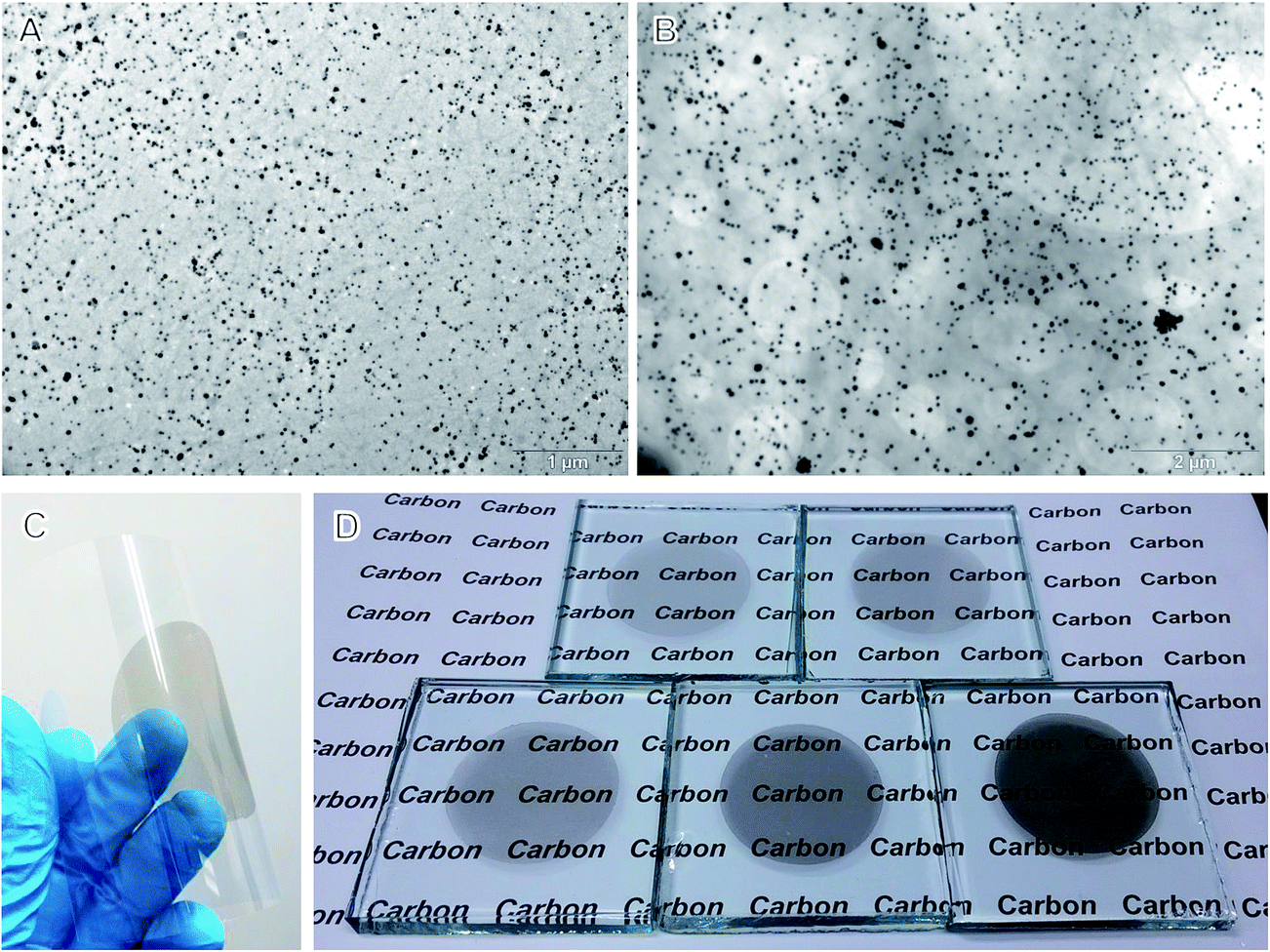 | ||
| Fig. 2 (A and B) TEM micrographs of continuous Ag–rGO film I and Ag–rGO film II. (C and D) Photographs of transferred Ag–rGO hybrid film II on PET and glass substrates. The films have a diameter of ∼4 cm. | ||
By controlling the volume of filtered suspension, electro-optical properties of the films can be readily tuned. Fig. 3A shows that the optical transmittance of both film I and film II is almost linearly dependent on the filtration volume. For filtration volume ≤ 700 ml, the transmittance is above ∼50% for film I with sheet resistance ranging between 40 Ω sq−1 and 32 MΩ sq−1 (Fig. 3B). For film II, the transmittance is above ∼40% with sheet resistance ranging between 11 Ω sq−1 and 16 kΩ sq−1 (Fig. 3B). At T = 75%, the sheet resistance is ∼30 Ω sq−1 for film II, which is much lower than that of rGO films (Fig. 3C). The dramatic reduction in sheet resistance indicates the effectiveness of Ag–rGO hybrid sheets as the building blocks for high-performance TCFs. XRD patterns of these hybrid films reveal that the peak at ∼26° (stacked graphene sheets) is missing (Fig. 3D), suggesting that most stacked rGO sheets (which are present in rGO film) are delaminated to accommodate the anchored AgNPs. Due to the huge amount of AgNPs (Fig. 1), numerous AgNP–rGO contacts are created accordingly. This would significantly alter the electrical transport properties of the rGO film, as will be discussed next.
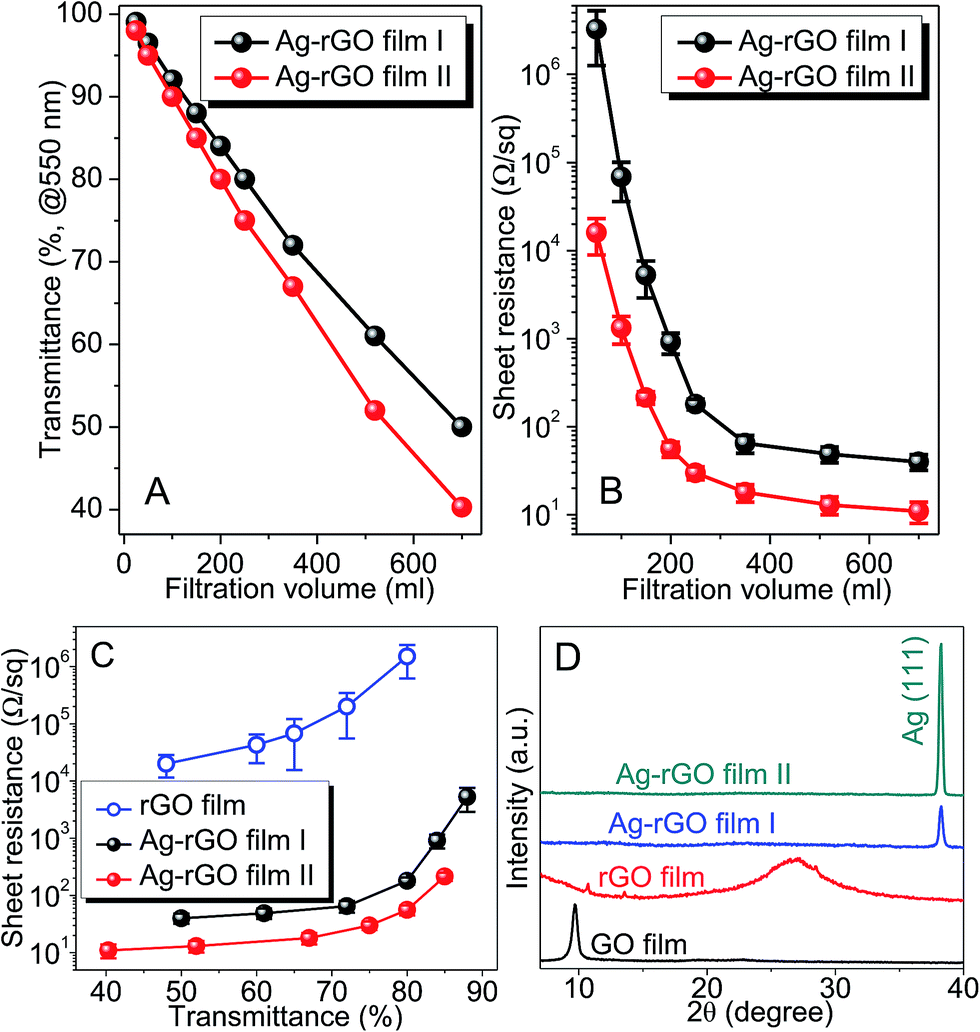 | ||
| Fig. 3 (A) Optical transmittance and (B) sheet resistance of Ag–rGO films as a function of filtration volume. (C) Comparison between sheet resistance–transmittance of rGO film and Ag–rGO films. Error bars show one standard deviation for 5 measurements. (D) XRD patterns of Ag–rGO film I and II on PET. XRD patterns of GO and rGO film are given for the purposes of comparison. | ||
The microstructure of these hybrid films was examined by SEM (Fig. 4). It showed that a huge number of AgNPs were evenly distributed in the hybrid films. The compactness of the films was maintained, indicating the transfer process would not negatively influence the film structure. Graphene possesses an intrinsic tensile strength of 130 GPa and in plane Young's modulus of 1 TPa,21 and excellent bending behavior due to its exceptionally low flexural rigidity.22 Therefore, the intimate contact between the Ag–rGO hybrid sheets in our films is considered of mechanical control in origin. This mechanical force reduces the air gap between these hybrid sheets and compresses them into an integrated continuous film, thereby improving AgNP–rGO contacts. Due to the larger sizes of incorporated AgNPs, thus Ag–rGO hybrid film II exhibits a relatively larger roughness (Fig. S4 and Table S1†). However, this should not pose a problem and can be effectively addressed by applying a thin polymer layer such as poly(3,4-ethylenedioxythiophene)/poly(styrenesulfonic acid) layer to smooth the surface for satisfying the needs of real applications.23
 | ||
| Fig. 4 (A and B) are low- and high-magnification SEM micrographs of Ag–rGO hybrid film I (∼88% transparency) on PET. (C, D and E) are low- and high-magnification SEM micrographs of Ag–rGO hybrid film II (∼80% transparency) on PET. | ||
The intimate contacts between AgNPs and rGOs would alter the electronic properties of both samples. Fig. 5A shows the Ag 3d5/2 and Ag 3d3/2 XPS spectra for both bulk Ag and Ag–rGO films. Two bands at 368 and 374 eV, ascribed to Ag 3d5/2 and Ag 3d3/2 binding energies, are identified for bulk Ag. These two bands shift remarkably to lower energies at 367.3 and 373.3 eV for Ag–rGO films. This 0.7 eV shift is caused by the electron transfer from AgNPs to rGO. It is known that the binding energy of the higher ionic state of Ag is lower than that of zero-valent Ag, due to shifts in the initial-state potential of ionic charge and the lattice potential. Since the work function of Ag (4.2 eV) is smaller than that of graphene (4.8 eV),24 electron transfer from AgNPs to rGO automatically occurs within the Ag–rGO hybrid films. This would effectively dope rGO with more electrons and raise its Fermi level above the conical point (Fig. 5B).
 | ||
| Fig. 5 (A) Ag 3d5/2 and Ag 3d3/2 XPS spectra of bulk Ag and Ag–rGO film I and Ag–rGO film II. (B) Energy band diagram of AgNP–rGO contact. (C) UPS spectra near the secondary-electron threshold region of rGO film, Ag–rGO film I and Ag–rGO film II. | ||
The phenomenon of electron transfer is further analyzed by UPS, as shown in Fig. 5C. The work function of rGO film, Ag–rGO film I and II can be determined from the spectra of second electron threshold. It can be found that the work function decreases from 4.8 eV for rGO film to 4.58 eV for Ag–rGO film I, and to 4.31 eV for Ag–rGO film II. The decrease in work function due to AgNPs incorporation into rGO indicates a change in the surface potential. It implies an upward shift of the Fermi level, which is consistent with the XPS results. As a result, a decrease in sheet resistance of Ag–rGO films can be attributed to the increased electron concentration due to n-doping by AgNPs. Considering the huge number of AgNPs within the hybrid films, this n-doping effect plays an important role in enhancing the film conductivity.
In addition to the n-doping effect, AgNPs would connect rGO sheets and “percolation” dope the rGO film. The concept of “percolation” doping was initially described for CVD-graphene when segregated domains were connected across grain boundaries by individual silver nanowires.10 Although rGO film is different from CVD-graphene, the highly resistive rGO–rGO junctions (Rj ≈ 150 MΩ)25 in rGO film are comparable to the grain boundaries in CVD-graphene. Electrically bridging adjacent or overlapped rGO sheets with AgNPs would, therefore, create additional conducting channels between these sheets and improve the transport properties of entire film. Due to the n-doping effect, silver–graphene junction is much more conductive. For weakly coupled silver–graphene junction, Rj ≈ 550 Ω; while for intimate silver–graphene contact, Rj ≈ 0 Ω.10 This same mechanism of “percolation” doping has been applied to improve the conductivity of rGO film by coupling it with sparse AgNW or copper nanowire (CuNW) network.15,26
The effects of electron doping and “percolation” doping on film conductivity can be well described by the resistor network model as illustrated in Fig. 6. The n-doping effect improve the conductivity of individual rGO sheets, whereas the “percolation” doping creates new conducting channels between adjacent or overlapped rGO sheets. A combination of these two effects leads to a drastic decrease in film resistance.
 | ||
| Fig. 6 Illustration of the resistor network model describing a four-layer stacked (A) rGO film and (B) Ag–rGO film. For rGO film, large resistance of individual rGO sheets and rGO–rGO junctions (Rj) result in a large sheet resistance. For Ag–rGO films, the resistance of rGO sheets decreases due to the n-doping effect, and AgNPs bridge the resistive rGO–rGO junctions. RrGO and RAg–rGO (<RrGO) denote the intrinsic resistance of individual rGO sheets and Ag–rGO hybrid sheets, respectively. | ||
In contrast to the flat transmittance–wavelength spectra of graphene films,27 the transmittance of Ag–rGO films shows a pronounced dependence on the light wavelength (Fig. 7), due to light absorption caused by surface plasma resonance (SPR) of AgNPs. This involves specific scattering interactions between the impinging light and the AgNPs. In particular, oscillating electric field of incoming light causes coherent oscillation of electrons in the conduction band of the nanoparticles, resulting in a concomitant oscillation of electron cloud surrounding the Ag nuclei. SPR generally causes light absorption at ∼410 nm.28,29 Nevertheless, the absorptions are highly dependent on the nanoparticle size, and the large AgNPs scatter predominantly in the forward direction (which is crucial for reducing surface reflectance), owing to the increase of radioactive efficiency and excitation of high-order modes.30 Therefore, Ag–rGO film II is more suitable for solar cell applications. AgNPs incorporated into the film can serve as an anti-reflection coating. They scatter more light into the cell and scatter at oblique angles to improve light-trapping, hence enhancing the device efficiency.30
 | ||
| Fig. 7 Optical transmittance of (A) Ag–rGO film I and (B) Ag–rGO film II at different sheet resistances. | ||
The relationship between transmittance and sheet resistance for Ag–rGO films and other nanostructured TCFs is plotted in Fig. 8A. At sheet resistances below ∼1.3 kΩ sq−1, films made from these Ag–rGO hybrid sheets are superior to similar films of rGOs and SWNTs made by spin coating and Mayer rod coating,14,31 respectively. At ∼75% transparency, the sheet resistance of Ag–rGO film II (30 Ω sq−1) is about 30 times lower than that of rGO film (∼1 kΩ sq−1). From the literature, continuous CVD-grown graphene films have superior performance to Ag–rGO films.8 However, they must be grown at a high temperature (1000 °C), and an additional step must be adopted to transfer graphene from metal substrates to non-conductive substrates. On the other hand, the lower processing temperatures and fabrication costs give Ag–rGO film a pronounced advantage over CVD-graphene in terms of cost consideration.
 | ||
| Fig. 8 (A) Plot of transmittance (at 550 nm) versus sheet resistance for films of Ag–rGO, rGO, CVD-graphene, SWNTs, AgNWs, CuNWs and ITO. (B) Plot of sheet resistance versus time for Ag–rGO hybrid films (80, 80 and 75% transparent from top to bottom) exposed to air for 50 days. (C) Plot of sheet resistance versus number of bends for Ag–rGO film I (80% transparency) and II (80% transparency) on PET. Error bars show one standard deviation for 5 measurements. | ||
Thin films of AgNWs and CuNWs also outperform Ag–rGO films in terms of electro-optical performance.32,33 However, the long-term electrical stability of these films is a major concern. Atmospheric sulfur tends to convert Ag into Ag2S, which is less conductive and has a stronger optical absorption.34 Copper is even more reactive, and it reacts with oxygen at ambient conditions and loses its conductivity more quickly.34 In order to examine the oxidation rate of Ag–rGO films, we exposed hybrid films with different conductivities in air and measured their sheet resistances periodically. Fig. 8B showed that over a period of 50 days, the sheet resistances remained fairly constant. There was a slight increase in the first week, but from the second week onward the sheet resistance remained within one standard deviation. This initial increase and subsequent stability is due to the oxidation of surficial AgNPs that are not covered by rGO. Although this is not a comprehensive test under a variety of environmental conditions, Fig. 8B illustrates that, even without any barrier materials to protect the films, they are fairly resistant to air oxidation.
Another advantage of Ag–rGO films is their excellent flexibility. To demonstrate this, Ag–rGO films on PET are subjected to both compressive and tensile bending cycles to a radius of curvature of ∼3 mm. Fig. 8C shows that these films exhibit little change in sheet resistance after 2000 bends. Such superior stability against bending deformation makes them very attractive for flexible electronic applications. By contrast, ITO on PET tends to lose its conductivity after just 50 bends,33 due to the formation of micro-cracks.35
Through enhanced chemical manipulation of solution-processable GO, the size and density of AgNPs can be more accurately controlled. This strategy plays an important role in achieving higher film conductivities per unit thickness, possibly allowing the use of thinner films to attain high transparency. Besides, the approach of vacuum filtration and transfer is a very slow process. Proper optimization of the rheological/wetting behavior of Ag–GO dispersions can be achieved through direct and scalable approaches such as rod coating. Further study of this will be presented elsewhere. The importance of realizing all these studies lies in the abundance, facile synthesis and relatively inexpensive nature of Ag–rGO when compared to SWNTs, CVD-graphene, AgNWs, CuNWs and ITO. Developing a precise control over growth of AgNPs on GO and more efficient film fabrication approaches will be the objectives of future research.
4. Conclusions
We have shown the potential of Ag–rGO as novel building blocks for fabricating transparent conductors. Compared to rGO films, Ag–rGO hybrid films showed a much lower sheet resistance at a given transparency. This was attributed to the n-doping and “percolation” doping effects of AgNPs, which increased the number of electrons within individual rGO sheets and reduced the rGO–rGO junction resistance. The electro-optical performance of Ag–rGO films was analyzed and compared with other TCFs, indicating that our films outperformed most carbonaceous films reported in the literature, especially rGO films. Although the synthesis scheme presented in this study was based on Ag–rGO, it can be extended to rGO decorated by other inexpensive metal nanoparticles, such as copper. The results presented in this study, in terms of utilizing water processable metal nanoparticle-decorated GO sheets as building blocks for fabricating films, open the opportunities for fabricating low-cost TCFs.Acknowledgements
This work is supported by a Strategic Grant (No. 7002772), City University of Hong Kong.References
- A. K. Geim and K. S. Novoselov, The rise of graphene, Nat. Mater., 2007, 6, 183–191 CrossRef CAS PubMed.
- J. B. Wu, M. Agrawal, H. A. Becerril, Z. N. Bao, Z. F. Liu, Y. S. Chen and P. Peumans, Organic light-emitting diodes on solution-processed graphene transparent electrodes, ACS Nano, 2010, 4, 43–48 CrossRef CAS PubMed.
- R. R. Nair, P. Blake, A. N. Grigorenko, K. S. Novoselov, T. J. Booth, T. Stauber, N. M. R. Peres and A. K. Geim, Fine structure constant defines visual transparency of graphene, Science, 2008, 320, 1308 CrossRef CAS PubMed.
- X. Li, Y. Zhu, W. Cai, M. Borysiak, B. Han, D. Chen, R. D. Piner, L. Colombo and R. Ruoff, Transfer of large-area graphene films for high-performance transparent conductive electrodes, Nano Lett., 2009, 9, 4359–4363 CrossRef CAS PubMed.
- L. He and S. C. Tjong, Aqueous graphene oxide-dispersed carbon nanotubes as inks for the scalable production of all-carbon transparent conductive films, J. Mater. Chem. C, 2016, 4, 7043–7051 RSC.
- L. He and S. C. Tjong, Nanostructured transparent conductive films: fabrication, characterization and applications, Mater. Sci. Eng., R, 2006, 109, 1–102 CrossRef.
- Y. Leterrier, L. Médico, F. Demarco, J.-A. E. Manson, U. Betz, M. F. Escola, M. Kharrazi and F. Atamny, Mechanical integrity of transparent conductive oxide films for flexible polymer-based displays, Thin Solid Films, 2004, 460, 156–166 CrossRef CAS.
- S. Bae, H. Kim, Y. Lee, X. Xu, J.-S. Park, Y. Zheng, J. Balakrishnan, T. Lei, H. R. Kim, Y. I. Song, Y.-J. Kim, K. S. Kim, B. Özyilmaz, J.-H. Ahn, B. H. Hong and S. Iijima, Roll-to-roll production of 30-inch graphene films for transparent electrodes, Nat. Nanotechnol., 2010, 5, 574–578 CrossRef CAS PubMed.
- J. Lee, K. S. Novoselov and H. S. Shin, Interaction between metal and graphene: dependence on the layer number of graphene, ACS Nano, 2010, 5, 608–612 CrossRef PubMed.
- R. Chen, S. R. Das, C. Jeong, M. R. Khan, D. B. Janes and M. A. Alam, Co-percolating graphene-wrapped silver nanowire network for high performance, highly stable, transparent conducting electrodes, Adv. Funct. Mater., 2013, 23, 5150–5158 CrossRef CAS.
- W. S. Hummers and R. E. Offeman, Preparation of graphitic oxide, J. Am. Chem. Soc., 1958, 80, 1339 CrossRef CAS.
- Q. Zheng, Z. Li, J. Yang and J.-K. Kim, Graphene oxide-based transparent conductive films, Prog. Mater. Sci., 2014, 64, 200–247 CrossRef CAS.
- H. Yamaguchi, G. Eda, C. Mattevi, H. K. Kim and M. Chhowalla, Highly uniform 300 mm wafer scale deposition of single and multilayered chemically derived graphene thin films, ACS Nano, 2010, 4, 524–528 CrossRef CAS PubMed.
- H. A. Becerril, J. Mao, Z. Liu, R. M. Stoltenberg, Z. Bao and Y. Chen, Evaluation of solution-processed reduced graphene oxide films as transparent conductors, ACS Nano, 2008, 2, 463–470 CrossRef CAS PubMed.
- I. N. Kholmanov, M. D. Stoller, J. Edgeworth, W. H. Lee, H. Li, J. Lee, C. Barnhart, J. R. Potts, R. Piner, D. Akinwande, J. E. Barrick and R. S. Ruoff, Nanostructured hybrid transparent conductive films with antibacterial properties, ACS Nano, 2012, 6, 5157–5163 CrossRef CAS PubMed.
- I. Pastoriza-Santos and L. M. Liz-Marzán, N,N-Dimethylformamide as a reaction medium for metal nanoparticle synthesis, Adv. Funct. Mater., 2009, 19, 679–688 CrossRef CAS.
- C. Gómez-Navarro, R. T. Weitz, A. M. Bittner, M. Scolari, A. Mews, M. Burghard and K. Kern, Electronic transport properties of individual chemically reduced graphene oxide sheets, Nano Lett., 2007, 7, 3499–3503 CrossRef PubMed.
- C. M. Niu, E. K. Sichel, R. Hoch, D. Moy and H. Tennent, High power electrochemical capacitors based on carbon nanotube electrodes, Appl. Phys. Lett., 1997, 70, 1480–1482 CrossRef CAS.
- G. Eda, G. Fanchini and M. Chhowalla, Large-area ultrathin films of reduced graphene oxide as a transparent and flexible electronic material, Nat. Nanotechnol., 2008, 3, 270–274 CrossRef CAS PubMed.
- S. Dubin, S. Gilje, K. Wang, V. C. Tung, K. Cha, A. S. Hall, J. Farrar, R. Varshneya, Y. Yang and R. B. Kaner, A one-step, solvothermal reduction method for producing reduced graphene oxide dispersions in organic solvents, ACS Nano, 2010, 7, 3845–3852 CrossRef PubMed.
- C. Lee, X. Wei, J. W. Kysar and J. Hone, Measurement of the elastic properties and intrinsic strength of monolayer grapheme, Science, 2008, 321, 385–388 CrossRef CAS PubMed.
- S. P. Koenig, N. G. Boddeti, M. L. Dunn and J. S. Bunch, Ultrastrong adhesion of graphene membranes, Nat. Nanotechnol., 2011, 6, 543–546 CrossRef CAS PubMed.
- D. S. Hecht, L. Hu and G. Irvin, Emerging transparent electrodes based on thin films of carbon nanotubes, graphene, and metallic nanostructures, Adv. Mater., 2011, 23, 1482–1513 CrossRef CAS PubMed.
- T. Wu, H. Shen, L. Sun, B. Cheng, B. Liu and J. Shen, Facile synthesis of Ag interlayer doped graphene by chemical vapor deposition using polystyrene as solid carbon source, ACS Appl. Mater. Interfaces, 2012, 4, 2041–2047 CAS.
- T. Bourgeteau, S. Le Vot, M. Bertucchi, V. Derycke, B. Jousselme, S. Campidelli and R. Cornut, New insights into the electronic transport of reduced graphene oxide using scanning electrochemical microscopy, J. Phys. Chem. Lett., 2014, 5, 4162–4166 CrossRef CAS PubMed.
- I. N. Kholmanov, S. H. Domingues, H. Chou, X. Wang, C. Tan, J.-Y. Kim, H. Li, R. Piner, A. J. G. Zarbin and R. S. Ruoff, Reduced graphene oxide/copper nanowire hybrid films as high-performance transparent electrodes, ACS Nano, 2013, 7, 1811–1816 CrossRef CAS PubMed.
- F. Bonaccorso, Z. Sun, T. Hasan and A. C. Ferrari, Graphene photonics and optoelectronics, Nat. Photonics, 2010, 4, 611–622 CrossRef CAS.
- M. Kerker, The optics of colloidal silver: something old and something new, J. Colloid Interface Sci., 1985, 105, 297–314 CrossRef CAS.
- C. G. Granqvist and R. A. Buhrman, Ultrafine metal particles, J. Appl. Phys., 1976, 47, 2200 CrossRef CAS.
- T. L. Temple, G. D. K. Mahanama, H. S. Reehal and D. M. Bagnal, Influence of localized surface plasmon excitation in silver nanoparticles on the performance of silicon solar cells, Sol. Energy Mater. Sol. Cells, 2009, 93, 1978–1985 CrossRef CAS.
- B. Dan, G. C. Irvin and M. Pasquali, Continuous and scalable fabrication of transparent conducting carbon nanotube films, ACS Nano, 2009, 3, 835–843 CrossRef CAS PubMed.
- S. De, T. M. Higgins, P. E. Lyons, E. M. Doherty, P. N. Nirmalraj, W. J. Blau, J. J. Boland and J. N. Coleman, Silver nanowire networks as flexible, transparent, conducting films: extremely high DC to optical conductivity ratios, ACS Nano, 2009, 3, 1767–1774 CrossRef CAS PubMed.
- A. R. Rathmell and B. J. Wiley, The synthesis and coating of long, thin copper nanowires to make flexible, transparent conducting films on plastic substrates, Adv. Mater., 2011, 23, 4798–4803 CrossRef CAS PubMed.
- S. Ye, A. R. Rathmell, Z. Chen, I. E. Stewart and B. J. Wiley, Metal nanowire networks: the next generation of transparent conductors, Adv. Mater., 2014, 26, 6670–6687 CrossRef CAS PubMed.
- D. R. Cairns, R. P. Witter, D. K. Sparacin, S. M. Sachsman, D. C. Paine, G. P. Crawford and R. R. Newton, Strain-dependent electrical resistance of tin-doped indium oxide on polymer substrates, Appl. Phys. Lett., 2000, 76, 1425 CrossRef CAS.
Footnote |
| † Electronic supplementary information (ESI) available. See DOI: 10.1039/c6ra26348h |
| This journal is © The Royal Society of Chemistry 2017 |