DOI:
10.1039/C6RA26342A
(Paper)
RSC Adv., 2017,
7, 9258-9263
Optimization of the window layer in large area silicon heterojunction solar cells
Received
5th November 2016
, Accepted 26th January 2017
First published on 30th January 2017
Abstract
Silicon heterojunction solar cells have shown great advantage due to their large open-circuit voltage which induces a high energy conversion efficiency. However, the short-circuit current density is limited by the high light absorption of an n-type amorphous silicon window layer in the short-wavelength range. Here an amorphous silicon oxide film was introduced to replace the window layer. The increasing oxygen content in amorphous silicon oxide layers leads to the enlarged optical band gap and the enhanced short-wavelength transmittance. As a result, the short-circuit current density increases obviously which comes from the high transmittance of amorphous silicon oxide films due to the wider band gap. Furthermore, the highly phosphorous-doped amorphous silicon layer was introduced to improve the contact between transparent conductive oxide layer and n-type amorphous silicon oxide layer. The carrier transport property is enhanced and thus the fill factor increases significantly. Finally, a silicon heterojunction solar cell with an area of 238.95 cm2 was prepared, yielding a total-area efficiency up to 21.1%. Overall, the results indicate that amorphous silicon oxide films can be applied to silicon heterojunction solar cells as a window layer, which provides a new route to obtain higher energy conversion efficiency.
1. Introduction
Silicon heterojunction (SHJ) solar cells are fabricated through depositing thin hydrogenated amorphous silicon (a-Si:H) layers on crystalline silicon substrates.1 Due to the outstanding passivation effect of the intrinsic a-Si:H films,2,3 SHJ solar cells show high open-circuit voltage (VOC) exceeding 750 mV![[thin space (1/6-em)]](https://www.rsc.org/images/entities/char_2009.gif) 3 which leads to high energy conversion efficiency.4 Upon the intrinsic a-Si:H films, doped (n-type or p-type) a-Si:H film is generally deposited to form a junction, which could separate the photo-generated carriers effectively.5 However, both the intrinsic and doped a-Si:H films contain lots of defects due to the presence of dangling bonds.6 In the respect of light absorption, it shows a high absorption in the short wavelength region (below 730 nm) due to the high absorption coefficient which comes from the quasi-direct band gap property of a-Si:H.7,8 Although the high absorption could lead to more photo-generated carriers, these carriers could not be pumped out due to the present of large density of defects.9 Z. C. Holman et al. pointed out that 70% carriers generated in intrinsic a-Si:H layers of heterojunctions recombined, and light absorbed in the doped a-Si:H layer had almost no contribution to short-circuit current density (JSC).9 So decreasing the parasitic absorption of a-Si:H layers is a key point to improve JSC. It has been demonstrated that decreasing the thickness of a-Si:H films is a useful method to improve JSC by decreasing absorption in short-wavelength region. However, the fill factor (FF) and VOC of SHJ solar cells decreased significantly because of the degrading of junction,10–12 the gain in JSC was offset by losses in FF and VOC.
3 which leads to high energy conversion efficiency.4 Upon the intrinsic a-Si:H films, doped (n-type or p-type) a-Si:H film is generally deposited to form a junction, which could separate the photo-generated carriers effectively.5 However, both the intrinsic and doped a-Si:H films contain lots of defects due to the presence of dangling bonds.6 In the respect of light absorption, it shows a high absorption in the short wavelength region (below 730 nm) due to the high absorption coefficient which comes from the quasi-direct band gap property of a-Si:H.7,8 Although the high absorption could lead to more photo-generated carriers, these carriers could not be pumped out due to the present of large density of defects.9 Z. C. Holman et al. pointed out that 70% carriers generated in intrinsic a-Si:H layers of heterojunctions recombined, and light absorbed in the doped a-Si:H layer had almost no contribution to short-circuit current density (JSC).9 So decreasing the parasitic absorption of a-Si:H layers is a key point to improve JSC. It has been demonstrated that decreasing the thickness of a-Si:H films is a useful method to improve JSC by decreasing absorption in short-wavelength region. However, the fill factor (FF) and VOC of SHJ solar cells decreased significantly because of the degrading of junction,10–12 the gain in JSC was offset by losses in FF and VOC.
Compared with a-Si:H films, hydrogenated amorphous silicon oxide (a-SiOx:H) films have much more advantages including wider band-gap and lower optical absorption.13 The absorption loss in short-wavelength region could be significantly reduced by adopting a-SiOx:H films and this strategy has worked in amorphous silicon solar cells.14,15 R. Biron et al. observed an enhancement of 0.6 mA cm−2 in JSC in the short-wavelength region due to the enlargement of optical band gap of silicon oxide based emitter,16 and other studies have obtained similar results.17,18 Here phosphorus-doped a-SiOx:H film was introduced to replace the n-type a-Si:H window layer. For the passivation layer, intrinsic a-Si:H film was left to keep an excellent passivation effect.19 The optical properties of n-type a-SiOx:H films and the effect of n-type a-SiOx:H films on SHJ solar cell performance were investigated in details. By adjusting the CO2/SiH4 flow ratio, the optimized oxygen content in a-SiOx:H films was obtained. Furthermore, highly phosphorous-doped a-Si:H films was introduced to improve the contact between transparent conducting oxide (TCO) and n-type a-SiOx:H layers, which improved the FF obviously. Finally, SHJ solar cell with large area of 238.95 cm2 was achieved, yielding a high efficiency of 21.1%. All these results obtained could be much useful to the industrial production of SHJ solar cell.
2. Experimental
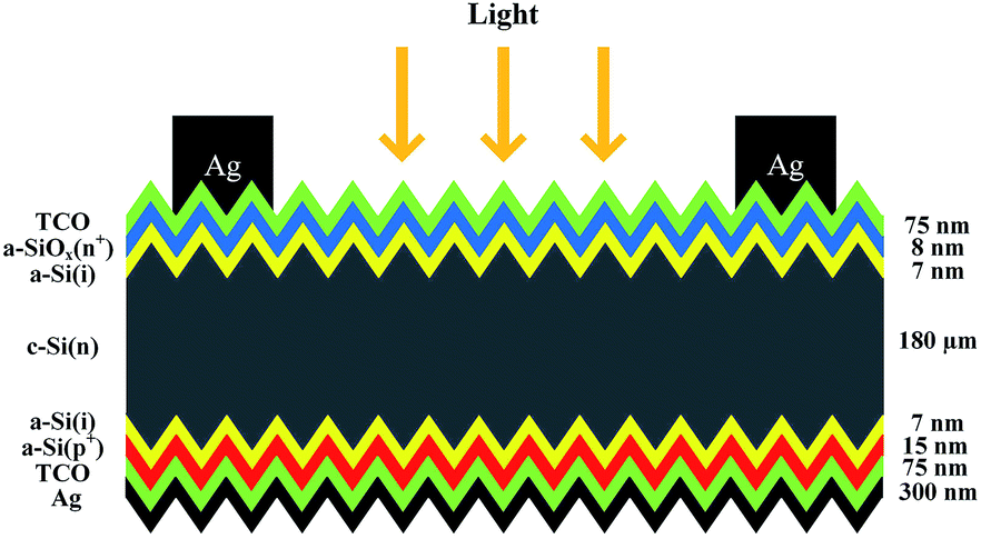
The a-Si/c-Si heterojunction solar cells were fabricated on commercial solar grade Czochralski silicon wafers (n type, 2–5 Ω cm, 200 μm thick, (100) oriented, 238.95 cm2 wafer size). Surface texture was formed wet-chemically by alkaline process (aqueous solution of potassium hydroxide (1.5% wt)), then cleaned by RCA process before transferred to deposition chamber. Very high frequency plasma enhanced chemical vapor deposition (VHF-PECVD, 40 MHz) reactor was used to prepare a-SiOx:H and a-Si:H films, the power density is 15 mW cm−2 and the deposition pressure is 30 Pa. The TCO layers (indium tin oxide, 10% wt SnO2-doped In2O3 ceramic target) and the silver back electrode were prepared by magnetron sputtering. Cells were finished with forming front electrodes by screen printing of silver paste. The structure of the a-Si/c-Si heterojunction solar cells is shown in Fig. 1.
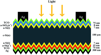 |
| | Fig. 1 The structure of the a-Si/c-Si heterojunction solar cells. | |
The current density–voltage (J–V) characteristics were obtained under standard test condition (STC, 25 °C, AM1.5G, 100 mW cm−2). External quantum efficiency (EQE) was used to evaluate the spectral response. Transmittance and reflectance were measured by PerkinElmer Lambda 950 spectrophotometer. Besides, a-SiOx:H and a-Si:H films were also investigated by Semilab PT-5 spectroscopic ellipsometry at room temperature using the Tauc-Lorentz method combined with the Bruggeman effective medium approximation (BEMA) model. Fourier transform infrared (FTIR) spectroscopy was used to verify the presence of oxygen for an approximately 100 nm thick layer. The one-sun (AM 1.5) photo-conductivity of different window n+-layers was measured by coplanar electrodes method using Keithley 2410, and the voltage applied between the two electrodes is 5 V. The length of the electrode is 16 mm and the spacing is 0.3 mm.
3. Results and discussion
3.1. Optical properties of n type a-SiOx:H
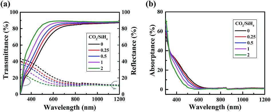
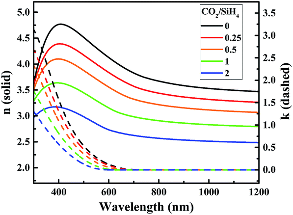
Fig. 2(a) presents the optical transmittance (T) and reflectance (R) spectra of n-type a-SiOx:H films with the same thickness of 8 nm deposited at various CO2/SiH4 flow ratios. It clearly shows that the transmittance of a-SiOx:H films increases with the increasing of CO2/SiH4 flow ratio in the wavelength from 300 to 1200 nm, especially in the region from 300 to 700 nm. The calculated absorptance (1 − T − R) result is shown in Fig. 2(b), where an obvious drop in the short-wavelength region is present with adjusting the CO2/SiH4 flow ratio. Fig. 3 represents the refractive indices (n) and extinction coefficients (k) of n-type a-SiOx:H films for an increasing CO2/SiH4 input flow ratio, derived from fitting spectroscopic ellipsometry data. It clearly shows that the refractive index decreases with the increase of CO2/SiH4 input flow ratio. This is the reason of the observed decrease of reflectance. It could be found that the extinction coefficient gradually decreases with the increase of CO2/SiH4 input flow ratio in the wavelength region from 300 nm to about 700 nm. As is known, extinction coefficient and absorption coefficient are positively correlated. Therefore, in the wavelength region from 300 nm to about 700 nm, the absorptance of a-SiOx:H films gradually decreases with the increase of CO2/SiH4 input flow ratio. In the wavelength region from 700 nm to 1200 nm, extinction coefficients are zero, indicating that a-SiOx:H films have no absorptance in this wavelength region. As a result of the differences in reflectance and absorptance, the transmittance of a-SiOx:H films increases with the increasing of CO2/SiH4 flow ratio in the wavelength from 300 to 1200 nm. Particularly in the wavelength region from 300 to 700 nm, due to the significant decrease of film absorptance, the increase of transmittance is more significant.
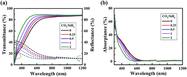 |
| | Fig. 2 Transmittance, reflectance (a) and absorptance (b) spectra of n-type a-SiOx:H films with various CO2/SiH4 flow ratios. | |
 |
| | Fig. 3 Refractive indices (n) and extinction coefficients (k) of n-type a-SiOx:H films with various CO2/SiH4 flow ratios derived from fitting spectroscopic ellipsometry data. | |
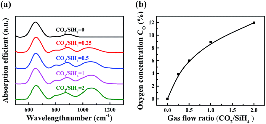
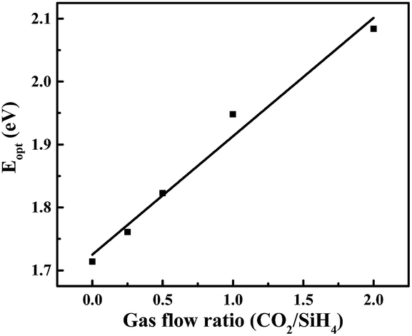
Fig. 4(a) shows the FTIR spectra of a-SiOx:H layers for various CO2/SiH4 input flow ratios. The absorption peak between 940 cm−1 and 1200 cm−1 represents the Si–O–Si stretching absorption band.20–22 It can be seen that the Si–O–Si stretching absorption gradually increases with the increase of CO2/SiH4 flow ratio. The oxygen concentration (CO, units of at%) in the a-SiOx:H films is estimated from the Si–O–Si stretching absorption band following G. Lucovsky et al.20 As is displayed in Fig. 4(b), the oxygen content gradually increases with the increase of CO2/SiH4 flow ratio. Because of higher bond energy of Si–O bonds,23–25 the optical band gap (Eopt) increases from 1.71 eV to 2.08 eV, which is shown in Fig. 5. The relationship between Eopt and absorption coefficient of a-SiOx:H layers is displayed in eqn (1),24,25 where B is a constant, ħω is the energy of photon. According to eqn (1), absorption coefficient of a-SiOx:H layers decreases with the widening of Eopt. So, the incorporation of oxygen in these films is the origination of the decreasing absorption in short wavelength region,19,23 this verifies the result of k presented in Fig. 3.
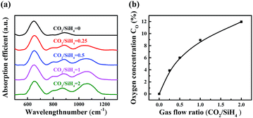 |
| | Fig. 4 FTIR spectra of a-SiOx:H layers for various CO2/SiH4 input flow ratios (a). Oxygen contents calculated from FTIR results (b). | |
 |
| | Fig. 5 Optical band gap as a function of CO2/SiH4 flow ratio. | |
3.2. Application of n-type a-SiOx:H in SHJ solar cells
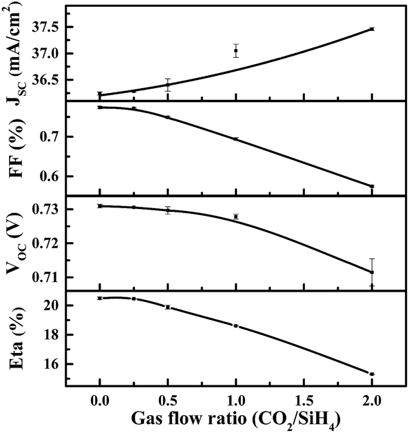
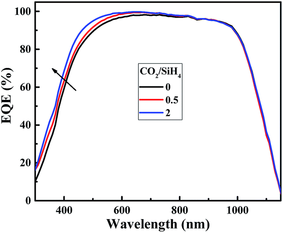
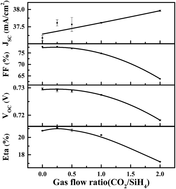
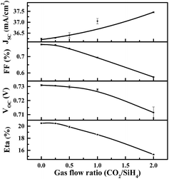
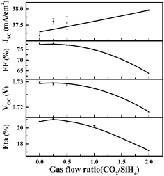
Fig. 6 shows the illuminated J–V results of solar cells featuring n-type a-SiOx:H window layers of various CO2/SiH4 flow ratios. As expected, JSC shows a trend of increase. As is shown in Fig. 7, the enhancement of JSC mainly originates from the improvement of spectral response in the short-wavelength region. This indicates that the high transmittance of a-SiOx:H layers in short-wavelength region indeed contributes to the JSC.
 |
| | Fig. 6 Illuminated J–V results of SHJ solar cells for various CO2/SiH4 input flow ratios. | |
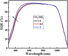 |
| | Fig. 7 EQE spectra of SHJ solar cells for various CO2/SiH4 input flow ratios. | |
As for VOC, a slight drop can be seen with the increase of CO2/SiH4 flow ratio. In this experiment, as the p side of the cell does not change, and n layers appear to have little detrimental effect on a-Si/c-Si chemical passivation quality.26 That means it is due to a loss in field effect passivation that the VOC goes down. It has been confirmed that fourfold coordinated phosphorus atoms become more unlikely with increasing oxygen content in a-SiOx:H films,27 and the fourfold coordination of phosphorus atoms is crucial for an effective doping.28 This indicates that the doping efficiency of phosphorous in a-SiOx:H film decreases with rising oxygen content, and Fermi level moves towards the direction of middle of band gap.28 As a result, the built-in voltage (Vbi) of the n+/n junction in thermal equilibrium gradually decreases. This will result in the degradation in field effect passivation, and the recombination of the photo-generated carriers increases. Finally, the density of electrons (n) and holes (p) reduces. EFn will move downwards with the decrease of electron density and EFp will move upwards with the decrease of hole density gradually. Therefore, the VOC which equal to quasi-Fermi splitting of electrons and holes continually reduces with the increase of CO2/SiH4 flow ratio.
With the increase of CO2/SiH4 flow ratio, energy conversion efficiency (Eta) gradually decreases. It can be easily found that the sharp decrease of FF is the main factor limiting the conversion efficiency of SHJ solar cell with n type a-SiOx:H film. In the next section, further analysis and corresponding optimization will be presented.
3.3. Improvement of cell performance by highly phosphorous-doped a-Si:H buffer layer
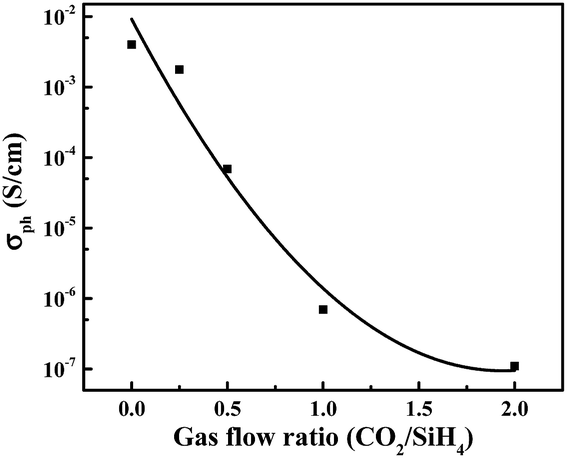
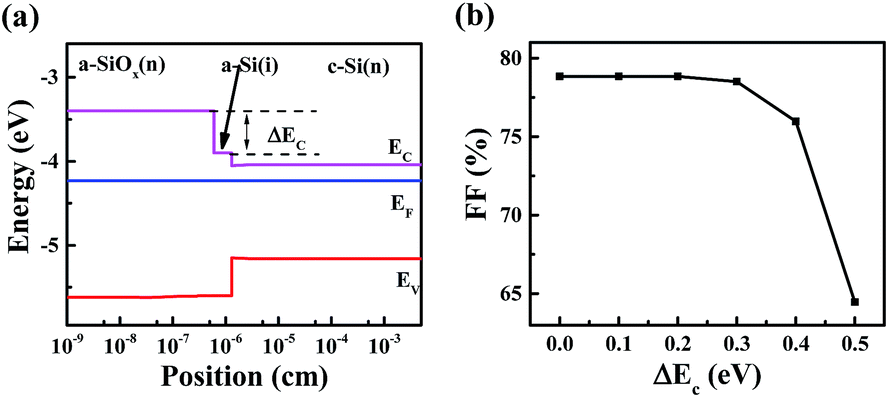
Generally, FF is affected by series resistance and parallel resistance. The replacement of a-Si:H with a-SiOx:H layer brings three changes including photo-conductivity (σph) of n+ layer, i/n+ interface band structure and TCO/n+ contact characteristic, which may weaken the transport of photo-generated carriers and result in the increase of series resistance. Fig. 8 shows the σph of phosphorous-doped a-SiOx:H layers as a function of CO2/SiH4 flow ratio. A gradual decrease in σph can be observed. The σph is related to the recombination of optically excited carriers, the observed decrease of σph is mainly due to the increase of the density of recombination centers.29–31 Moreover, the decreased doping efficiency of phosphorous and increasingly intrinsic character with the increase of oxygen content will affect the σph.28,32,33 In order to obtain high transmittance, the cost of low σph cannot be avoided for a-SiOx:H films. Additionally, the increase in Eopt with increasing CO2/SiH4 flow ratio results in the enlargement in the band offset at the i/n interface.34 In this experiment, electrons are collected at the front, an increasing conduction band offset (ΔEc, shown in Fig. 9 (a)) at the interface between intrinsic a-Si:H layer and n-type a-SiOx:H layer may be detrimental, resulting in less efficient transport of carriers. Meantime, the increase of oxygen in n-type a-SiOx:H layer results in the decrease of carrier density and drop of Fermi level. Therefore, the contact between n+ layer and TCO layer is also affected. This may also limit the transport of photo-generated carriers.
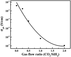 |
| | Fig. 8 The photoconductivity of phosphorous-doped a-SiOx:H layers as a function of CO2/SiH4 flow ratio. | |
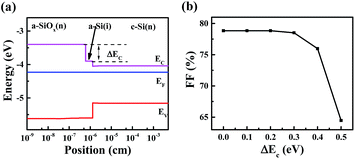 |
| | Fig. 9 Energy band diagram at the i/n interface (a), simulated FF as a function of conduction band offset (b). | |
In order to investigate the influence of ΔEc on the transport characteristic of photo-generated electrons, AFORS-HET was used to simulate the device performance. The contacts between TCO and a-Si:H (p+ and n+) were assumed as flat band to neglect the potential contact influence, and the Fermi level and the valence band bottom of the a-SiOx:H layer were assumed to be fixed to neglect the potential valence band offset influence. Detailed information of the substrate and amorphous silicon layers could be found in Table 1, the simulation result is shown in Fig. 9(b). From Fig. 9(b), the FF does not show a sharp decrease until ΔEc is larger than 0.4 eV, the value is similar to that other groups have concluded.35,36 In this experiment, the band gap of intrinsic a-Si:H is approximately 1.71 eV, and the band gap of n-type a-SiOx:H layers changes from 1.71 eV to 2.08 eV. This means that the ΔEc at the i/n+ interface would not exceed 0.185 eV (half of the band gap difference), since ΔEc is usually smaller than valance band offset (ΔEv).37–41 That is to say, the i/n+ interface band offset will not lead to the significant decrease of FF. So, the contact between phosphorous-doped a-SiOx:H layer and TCO layer may be more responsible for the decrease of FF.
Table 1 The set of values for the simulation of the SHJ solar cells
| Parameters |
a-SiOx (n) |
a-SiH (p) |
i-layer |
c-Si |
| Dielectric constant |
11.9 |
11.9 |
11.9 |
11.9 |
| Thickness (nm) |
8 |
15 |
7 |
2 × 10⁵ |
| Electron affinity (eV) |
3.4–3.9 |
3.9 |
3.9 |
4.05 |
| Band gap (eV) |
1.71–2.21 |
1.71 |
1.71 |
1.12 |
| Effective conduction band density (cm−3) |
1 × 10²⁰ |
1 × 10²⁰ |
1 × 10²⁰ |
2.85 × 10¹⁹ |
| Effective valence band density (cm−3) |
1 × 10²⁰ |
1 × 10²⁰ |
1 × 10²⁰ |
2.69 × 10¹⁹ |
| Doping concentration of acceptors (cm−3) |
0 |
8.30 × 10¹⁹ |
0 |
0 |
| Doping concentration of donors (cm−3) |
6.90 × 10¹⁹ |
0 |
0 |
1.5 × 10¹⁶ |
| Thermal velocity of electrons (cm s−1) |
1 × 10⁷ |
1 × 10⁷ |
1 × 10⁷ |
1 × 10⁷ |
| Thermal velocity of holes (cm s−1) |
1 × 10⁷ |
1 × 10⁷ |
1 × 10⁷ |
1 × 10⁷ |
| Layer density (g cm−3) |
2.328 |
2.328 |
2.328 |
2.328 |
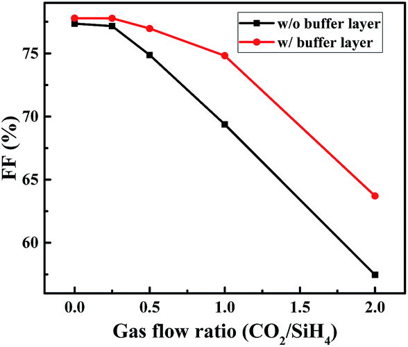
In a next step, solar cells with a highly phosphorous-doped a-Si:H buffer layer (2 nm) between the TCO layer and n-type a-SiOx:H layer were prepared. The PH3/SiH4 flow ratio was 3% for the a-Si:H buffer layers, while 1.5% for the n-type a-SiOx:H layers. Fig. 10 shows the illuminated I–V parameters of solar cells with highly doped a-Si:H buffer layers. The basic trends of VOC, JSC and FF do not change, but Fig. 11 clearly shows that the decrease amplitude of FF significantly reduces due to the introduction of highly phosphorous doped a-Si:H buffer layer. When the CO2/SiH4 flow ratio increases from 0 to 2, FF shows varying degrees of improvement. Due to the improvement of FF and JSC, the conversion efficiency increases slightly when CO2/SiH4 flow ratio is relatively low. Results indicate that the highly phosphorous doped a-Si:H buffer layer improves the TCO/n contact characteristic due to higher carrier density and higher Fermi level.42–51
 |
| | Fig. 10 Illuminated J–V results of SHJ solar cells with highly phosphorous doped a-Si:H buffer layer. | |
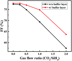 |
| | Fig. 11 FF as a function of CO2/SiH4 flow ratio with and without highly phosphorous doped a-Si buffer layer. | |
Finally, a total-area conversion efficiency of 21.1% was achieved on 238.85 cm2 SHJ solar cell when the CO2/SiH4 flow ratio is 0.25. Compared with the standard cell, it exhibits a relative improvement of 2% in conversion efficiency at room temperature. Generally, the standard cell (a-Si:H n+ layer) would show a decrease in FF when increasing the temperature, whereas the cell with an oxide layer recovers gradually.19,52 This means the a-SiOx:H cell has a low temperature coefficient, which might show a big advantage in the real power generation process.
4. Conclusions
In summary, n-type a-SiOx:H layers were prepared and applied to SHJ solar cells as window n+ layers. The VOC decreases slightly with the increase of CO2/SiH4 flow ratio, this may be caused by the dropping of Fermi level which is originated from gradually decreased phosphorous doping efficiency. The application of such layers decreases the n+ layers' absorption in short wavelength region, resulting in improvement in JSC. Moreover, through the insertion of a-Si:H buffer layer, the contact between TCO layer and a-SiOx:H layer is greatly improved. The best SHJ solar cell with a-SiOx:H layer reached an efficiency of 21.1% (VOC: 729 mV, JSC: 37.6 mA cm−2, FF: 77.0%, cell area: 238.95 cm2). The application of wide band-gap a-SiOx:H layers on SHJ solar cells shows potential in improving conversion efficiency, the optimal parameters of a-SiOx:H layers need further research for a higher conversion efficiency in the future.
Acknowledgements
This work was supported by the National Natural Science Foundation of China (51302081, 61575010, 61574009, 11274028, 11574014), Beijing Nova Program (Z141109001814053) and the Science and Technology Commission of Beijing Municipality (Z151100003315018, Z151100003515004). Authors appreciate Mr Mingfang Dai, Dr Yuanmin Li, Dr Hui Zhao, Ms. Lan Chen at Hanergy Thin Film Solar Group, R&D Center, for great support and helpful discussions. Authors also acknowledge all the colleagues in Thin Film Lab of Beijing University of Technology.
Notes and references
- S. De Wolf, A. Descoeudres, Z. C. Holman and C. Ballif, Green, 2012, 2, 7–24 CrossRef CAS.
- X. Y. Zhang, S. Hargreaves, Y. M. Wan and A. Cuevas, Phys. Status Solidi RRL, 2014, 8, 231–234 CrossRef CAS.
- M. Taguchi, A. Yano, S. Tohoda, K. Matsuyama, Y. Nakamura, T. Nishiwaki, K. Fujita and E. Maruyama, IEEE Journal of Photovoltaics, 2014, 4, 96–99 CrossRef.
- A. Descoeudres, L. Barraud, S. De Wolf, B. Strahm, D. Lachenal, C. Guerin, Z. C. Holman, F. Zicarelli, B. Demaurex, J. Seif, J. Holovsky and C. Ballif, Appl. Phys. Lett., 2011, 99, 123506 CrossRef.
- A. Cuevas and D. Yan, IEEE Journal of Photovoltaics, 2013, 3, 916–923 CrossRef.
- J. Ramanujam and A. Verma, Mater. Express, 2012, 2, 177–196 CrossRef CAS.
- M. Vanecek, J. Kocka, J. Stuchlik and A. Triska, Solid State Commun., 1981, 39, 1199–1202 CrossRef CAS.
- E. Fefer, Y. Shapira and I. Balberg, Appl. Phys. Lett., 1995, 67, 371–373 CrossRef CAS.
- Z. C. Holman, A. Descoeudres, L. Barraud, F. Z. Fernandez, J. P. Seif, S. De Wolf and C. Ballif, IEEE Journal of Photovoltaics, 2012, 2, 7–15 CrossRef.
- H. Fujiwara and M. Kondo, J. Appl. Phys., 2007, 101, 054516 CrossRef.
- M. Tanaka, M. Taguchi, T. Matsuyama, T. Sawada, S. Tsuda, S. Nakano, H. Hanafusa and Y. Kuwano, Jpn. J. Appl. Phys., 1992, 31, 3518–3522 CrossRef CAS.
- M. R. Page, E. Iwaniczko, Y. Q. Xu, L. Roybal, F. Hasoon, Q. Wang and R. S. Crandall, Thin Solid Films, 2011, 519, 4527–4530 CrossRef CAS.
- H. Watanabe, K. Haga and T. Lohner, J. Non-Cryst. Solids, 1993, 164–166, 1088 Search PubMed.
- P. Cuony, M. Marending, D. T. L. Alexander, M. Boccard, G. Bugnon, M. Despeisse and C. Ballif, Appl. Phys. Lett., 2010, 97, 143505 CrossRef.
- V. Smirnov, W. Böttler, A. Lambertz, H. Wang, R. Carius and F. Finger, Phys. Status Solidi C, 2010, 7, 1053–1056 CAS.
- R. Biron, C. Pahud, F. J. Haug, J. Escarre, K. Soderstrom and C. Ballif, J. Appl. Phys., 2011, 110, 124511 CrossRef.
- J. Park, V. A. Dao, C. Shin, H. Park, M. Kim, J. Jung, D. Kim and J. Yi, Thin Solid Films, 2013, 546, 331–336 CrossRef CAS.
- P. Sichanugrist, T. Sasaki, A. Asano, Y. Ichikawa and H. Sakai, Sol. Energy Mater. Sol. Cells, 1994, 34, 415–422 CrossRef CAS.
- J. Peter Seif, A. Descoeudres, M. Filipič, F. Smole, M. Topič, Z. Charles Holman, S. De Wolf and C. Ballif, J. Appl. Phys., 2014, 115, 024502 CrossRef.
- G. Lucovsky, J. Yang, S. S. Chao, J. E. Tyler and W. Czubatyj, Phys. Rev. B: Condens. Matter Mater. Phys., 1983, 28, 3225–3233 CrossRef CAS.
- S. J. Wen, G. Campet, J. Portier, G. Couturier and J. B. Goodenough, Mater. Sci. Eng., B, 1992, 14, 115–119 CrossRef.
- M. Niwano, J. Kageyama, K. Kinashi, N. Miyamoto and K. Honma, J. Vac. Sci. Technol., A, 1994, 12, 465–470 CAS.
- D. Das, S. M. Iftiquar and A. K. Barua, J. Non-Cryst. Solids, 1997, 210, 148–154 CrossRef CAS.
- J. E. Lee, J. H. Park, J. Yoo, K. H. Yoon, D. Kim and J. S. Cho, Solid State Sci., 2013, 20, 70–74 CrossRef CAS.
- M. Koos, I. Pocsik and I. K. Somogyi, J. Non-Cryst. Solids, 1987, 90, 469–471 CrossRef CAS.
- S. De Wolf and M. Kondo, J. Appl. Phys., 2009, 105, 103707 CrossRef.
- K. Hubner, Phys. Status Solidi A, 1980, 61, 665–673 CrossRef.
- A. Janotta, R. Janssen, M. Schmidt, T. Graf, M. Stutzmann, L. Görgens, A. Bergmaier, G. Dollinger, C. Hammerl, S. Schreiber and B. Stritzker, Phys. Rev. B: Condens. Matter Mater. Phys., 2004, 69, 115206 CrossRef.
- T. Itoh, R. Katayama, K. Yamakawa, K. Matsui, M. Saito, S. Sugiyama, P. Sichanugrist, S. Nonomura and M. Konagai, Jpn. J. Appl. Phys., 2015, 54, 08KB11 CrossRef.
- M. C. Rossi, M. S. Brandt and M. Stutzmann, Appl. Surf. Sci., 1996, 102, 323–326 CrossRef CAS.
- J.-J. Park, Y.-K. Kim, S.-W. Lee, Y.-J. Lee, J.-S. Yi, S. Q. Hussain and N. Balaji, Transactions on Electrical and Electronic Materials, 2012, 13, 192–195 CrossRef.
- W. Y. Ching, Phys. Rev. B: Condens. Matter Mater. Phys., 1980, 22, 2816–2822 CrossRef CAS.
- D. Das and A. K. Barua, Sol. Energy Mater. Sol. Cells, 2000, 60, 167–179 CrossRef CAS.
- T. F. Schulze, L. Korte, F. Ruske and B. Rech, Phys. Rev. B: Condens. Matter Mater. Phys., 2011, 83, 165314 CrossRef.
- M. Liebhaber, M. Mews, T. F. Schulze, L. Korte, B. Rech and K. Lips, Appl. Phys. Lett., 2015, 106, 031601 CrossRef.
- M. Rahmouni, A. Datta, P. Chatterjee, J. Damon-Lacoste, C. Ballif and P. R. I. Cabarrocas, J. Appl. Phys., 2010, 107, 054521 CrossRef.
- H. Mimura and Y. Hatanaka, Appl. Phys. Lett., 1987, 50, 326–328 CrossRef CAS.
- H. Eschrich, J. Bruns, L. Elstner and C. Swiatkowski, J. Non-Cryst. Solids, 1993, 166, 717–720 CrossRef.
- J. M. Essick and J. D. Cohen, Appl. Phys. Lett., 1989, 55, 1232–1234 CrossRef CAS.
- W. Fuhs, L. Korte and M. Schmidt, J. Optoelectron. Adv. Mater., 2006, 8, 1989–1995 CAS.
- M. Schmidt, L. Korte, A. Laades, R. Stangl and C. H. Schubert, Thin Solid Films, 2007, 515, 7475–7480 CrossRef CAS.
- R. Timmreck, S. Olthof, K. Leo and M. K. Riede, J. Appl. Phys., 2010, 108, 033108 CrossRef.
- A. N. Corpus-Mendoza, M. M. De Souza and F. U. Hamelmann, IEEE Journal of Photovoltaics, 2015, 5, 22–27 CrossRef.
- P. D. Veneri, L. V. Mercaldo and I. Usatii, Appl. Phys. Lett., 2010, 97, 023512 CrossRef.
- J. Sritharathikhun, H. Yamamoto, S. Miyajima, A. Yamada and M. Konagai, Jpn. J. Appl. Phys., 2008, 47, 8452–8455 CrossRef CAS.
- A. Kanevce and W. K. Metzger, J. Appl. Phys., 2009, 105, 094507 CrossRef.
- M. Tucci, L. Serenelli, S. De Iuliis, M. Izzi, G. de Cesare and D. Caputo, in Physics and Technology of Amorphous-Crystalline Heterostructure Silicon Solar Cells, ed. W. G. J. H. M. van Sark, L. Korte and F. Roca, Springer Berlin Heidelberg, Berlin, Heidelberg, 2012, pp. 331–375, DOI:10.1007/978-3-642-22275-7_10.
- L. V. Mercaldo, I. Usatii and P. D. Veneri, Energies, 2016, 9, 218 CrossRef.
- J. J. Liou, IEE Proceedings, Part G: Circuits, Devices and Systems, 1992, 139, 646–654 CrossRef.
- A. Blicher, Rep. Prog. Phys., 1982, 45, 427–468 CrossRef.
- J. Wang, H. B. Wang, J. Zhang, X. J. Yan and D. H. Yan, J. Appl. Phys., 2005, 97, 026106 CrossRef.
- M. W. M. van Cleef, F. A. Rubinelli, R. Rizzoli, R. Pinghini, R. E. I. Schropp and W. F. van der Weg, Jpn. J. Appl. Phys., 1998, 37, 3926–3932 CrossRef CAS.
|
| This journal is © The Royal Society of Chemistry 2017 |
Click here to see how this site uses Cookies. View our privacy policy here. 
 Open Access Article
 This Open Access Article is licensed under a
  *a,
Xuemei Songa and
Hui Yan*a
*a,
Xuemei Songa and
Hui Yan*a