
 Open Access Article
 This Open Access Article is licensed under a
 Creative Commons Attribution 3.0 Unported Licence
Ultra-narrow blue phosphorene nanoribbons for tunable optoelectronics†
Ram Swaroopa,
P. K. Ahluwaliab,
K. Tankeshwarc and
Ashok Kumar *a
*a
aCentre for Physical Sciences, School of Basic and Applied Sciences, Central University of Punjab, Bathinda, Punjab 151001, India. E-mail: ashok@cup.ac.in
bDepartment of Physics, Himachal Pradesh University, Shimla, Himachal Pradesh 171005, India
cDepartment of Physics, Guru Jambheshwar University of Science and Technology, Hisar, Haryana 125001, India
First published on 13th January 2017
Abstract
We report optoelectronic properties of ultra-narrow blue phosphorene nanoribbons (BPNRs) within the state-of-the-art density functional theory framework. The positive but small value of formation energy (∼0.1 eV per atom) indicates the relative ease of the formation of BPNRs from their two-dimensional (2D) counterpart. The oscillatory behaviour of the electronic band gap of bare BPNRs with increasing width is attributed to the reconstruction of edge atoms. The static dielectric constant of BPNRs depends on the width and applied strain which in turn shows consistency with the Penn's model expression for semiconductors. Bare BPNRs exhibit both π and π + σ plasmonic structures while passivated ones possess only a π + σ plasmonic structure that get blue-shifted (as large as ∼3 eV) on increasing the width of the BPNRs which makes electron energy loss spectroscopy useful for identifying the width of BPNRs in real experimental situations. The mechanical strain induces a small red shift in, which is attributed to the modification in electronic band dispersion due to a different superposition of atomic orbitals on the application of applied strain. These tunable electronic and dielectric properties of BPNRs mean they may find applications in optoelectronic devices based on blue phosphorene.
1. Introduction
After the discovery of graphene in 2004, it became the world's first two dimensional (2D) stable crystal with a honeycomb structure.1 Graphene possess unique electronic and mechanical properties along with high carrier mobility, even greater than Si at room temperature.2–4 Graphene gave rise to a new era of low dimensional materials, consequently, new classes of 2D materials such as silicene,5,6 germanene,7 transition metal dichalcogenide (TMDs)8–10 etc. were predicted and have been realised experimentally. TMDs exist in variety of forms ranging from metals to wide-gap semiconductors.3 Group-IV elemental layers are found to exhibit zero band-gap which limits their applications in the semiconductor industry, while their functionalization leads to semiconducting behaviour.11Recently, 2D atomic layer of phosphorus atoms known as black- or α-phosphorene, with inherent band gap ∼2 eV has emerged as a potential candidate for semiconductor electronics.12–14 Phosphorene-based transistor demonstrates high carrier mobility with higher on/off ratio (≈104) at room temperature.15 Electronic band gap of black phosphorene is found to vary inversely with thickness of the layers.16 Also phosphorene exhibits four thermodynamically stable allotropic forms namely black (α)-, blue (β)-, gamma (γ)- and delta (δ)-phosphorene, out of these, black (α)- and blue (β)-phosphorene are found to be most stable.17,18 The various structural phases of phosphorene show tunability in electronic structure on the application of external electric field, strain and pressure.19–21
It is well known that electronic properties change significantly when one goes from 2D monolayer to 1D nanoribbons (NRs). Note that in laboratory situation graphene nanoribbons have been fabricated in controlled fashion by various synthesis techniques.22–25 The electronic properties of phosphorene NRs show strong dependence on their width and edge structure.26–28 The electronic band gap of NRs changes on functionalization of edges with various functional groups.29,30 Also it is found that electronic band gap varies inversely to the width of NRs.26 Furthermore, electronic properties are strongly influenced by the orientation of nanoribbons.31 Mechanical strain and perpendicular electric field also modify the electronic band gap of black phosphorene NRs.31,32
Interestingly, ultra-narrow width armchair graphene NRs as narrow as five carbon atoms, have been successfully synthesized and characterized by the low temperature scanning tunnelling microscopy.33 Ultra-narrow ribbons have been found to show nearly metallic nature with delocalized orbitals. These ultra-narrow width ribbons have been suggested to be used as interconnects in devices in place of Cu. Similarly, ultra-narrow graphene bilayer nanoribbons obtained by unzipping of multiwall carbon nanotube have been characterized under high magnetic field which show Landau quantization.34
Although numerous studies have been made to understand the various properties of black phosphorene nanoribbon,26–31 with less attention paid to blue phosphorene based nanoribbons. Here we present a detailed study of ultra-narrow blue phosphorene nanoribbons of varying width with armchair and zigzag edge configurations. The effect of width and mechanical strain on the electronic and dielectric properties of ultra-narrow blue phosphorene NRs have been discussed. The effect of hydrogen passivation at the edges of the considered NRs is also investigated in detail.
2. Computational methods
First principles calculations are performed within density functional theory framework as implemented in SIESTA (Spanish Initiative for Electronic Simulations with Thousands of Atoms) simulation package.35–37 Norm conserving Troullier Martin pseudo-potential in fully separable Kleinman and Bylander form has been used to treat the electron–ion interactions.38 The exchange and correlation energies have been treated within the General Gradient Approximation (GGA) according to the Perdew–Burke–Ernzerhof (PBE) parameterization.39 The Kohn Sham orbital's were expanded in a linear combination of numerical pseudo atomic orbital's using a split-valence double zeta basis set with polarization functions (DZP).Throughout geometry optimization confinement energy of numerical pseudo-atomic orbital's are taken as 0.01 Ry. Minimization of energy was carried out using standard conjugate-gradient (CG) technique. Structures were relaxed until the forces on each atom were less than 0.01 eV Å−1. Monkhorst–Pack scheme is used to sample Brillouin zone with a 10 × 1 × 1 mesh. The spacing of the real space used to calculate the Hartree, exchange and correlation contribution of the total energy and Hamiltonian was 450 Ry. The distance between the periodic images in non-periodic direction of ribbons is kept more than 10 Å to avoid the mutual interaction between the images.
Optical broadening of 0.2 eV was used for dielectric properties calculations. All the unoccupied states have been considered for the calculations of optical spectra. The imaginary part of dielectric function (ε2) has been estimated by calculating the dipolar transition matrix elements between occupied and unoccupied single electron eigenstates.35 The real part of dielectric function (ε1) has been obtained using Kramers–Kroning transformations. Finally, the Electron Energy Loss Spectra (EELS) was calculated using ε1 and ε2 in the following formula:
 | (1) |
3. Results and discussions
Blue phosphorene possess graphene-like honeycomb structure with 0.59 Å out-of-plan buckling of P-atoms. Our GGA-PBE calculated lattice constant 3.31 Å is in excellent agreement with previously reported value 3.33 Å.17,18 The cohesive energy of blue and black phosphorene was found to be nearly same (ΔE ∼ 1 meV per atom),17 suggesting both allotropic layers to be equally stable. Our calculated indirect band gap of 2.02 eV is also in excellent agreement with the previously reported value ∼2 eV at GGA-PBE level of theory.17,18Similar to graphene NRs, blue phosphorene nanoribbons (BPNRs) can be obtained by cutting monolayer blue phosphorene along armchair (AC) or zigzag (ZZ) directions. The width of the armchair blue phosphorene nanoribbon (ABPNR) and zigzag blue phosphorene nanoribbon (ZBPNR) can be identified by counting number of atomic lines (n) of P atoms across the ribbon. The ball and stick model of ABPNR and ZBPNR is shown in Fig. 1, where we have considered width (n) from 2 to 12. Note that various configurations of edge structures are possible in nanoribbons,40–44 however, armchair and zigzag edges are most common stable configurations for graphene-like nanoribbons. In case of graphene nanoribbons, zigzag-57 (stone-wales defected) edge structure were reported to be most stable with very small energy difference (0.02 eV Å−1) relative to armchair edge structure.42 To introduce stone wales defects, one need to consider wider and long ribbon to mimic the structural defects in nanoribbons.
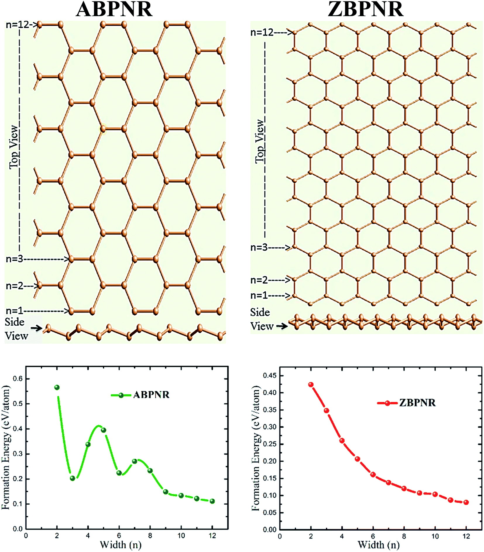 | ||
| Fig. 1 Top and side view of armchair blue phosphorene nanoribbon (ABPNR) and zigzag blue phosphorene nanoribbon (ZBPNR), where ‘n’ represent the number of atomic lines in nanoribbons (top panel). Formation energy as a function of width is plotted in bottom panel. | ||
Furthermore, the edges are passivated with hydrogen atoms as shown in Fig. S1 of ESI.† On structure relaxation of bare ribbons, the atoms on the edges of both ABPNR and ZBPNR get reconstructed. The reconstruction of atoms for lower width ribbons (n < 6) is found to be more pronounced than wider ribbons (Fig. S2 and S3 of ESI†). In order to investigate the relative stability of BPNRs, we have computed the formation energy of both ABPNRs and ZBPNRs. The formation energy (EF) is defined as:
 | (2) |
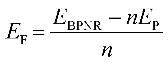
Similar to monolayer blue phosphorene, both ABPNR and ZBPNR exhibit semiconducting character, however, with smaller band gap. The electronic band structure of ABPNR at n = 12 show 1.16 eV direct band gap while ZBPNR possess indirect band gap 0.58 eV at the same width at GGA-PBE level of theory [Fig. 2]. The states around the Fermi energy are due to the dangling bonds present at the edges of nanoribbons. The band gap for H-passivated edges of ABPNR and ZBPNR is calculated as 2.18 eV and 2.05 eV, respectively, using GGA-PBE functional [Fig. 2].
 | ||
| Fig. 2 Electronic band structure and corresponding density of states of armchair blue phosphorene nanoribbon (ABPNR), zigzag blue phosphorene nanoribbon (ZBPNR) and hydrogen passivated edges structures (H-ABPNR and H-ZBPNR) at width n = 12. | ||
3.1 Width-dependent electronic properties of BPNRs
Electronic properties of both ABPNR and ZBPNR show distinct behaviour on varying the width (n) of ribbons, e.g., the electronic band gap of ABPNR as function of width show oscillatory behaviour for n ≤ 9, while at higher width the band gap remain nearly constant (∼1 eV) (Fig. 3(a)); ZBPNR show metallic characteristics for n ≤ 5 and semiconducting features (Eg ∼ 0.1 eV) at higher width (n = 6–9). The oscillatory behaviour in the electronic band gap for both kind of ribbons may be attributed to the reconstruction of edge atoms as shown in Fig. S2 & S3 of ESI,† which is more pronounced for lower width bare BPNRs. It is evident from Fig. 3(b) and (c) that dispersion of bands around Fermi energy due to unsaturated bonds gets modified significantly on varying the width that results into change in the electronic behaviour of ribbons. Note that the oscillatory behaviour of electronic band gap of nanoribbons at lower width has also been observed in previous studies.26–28 | ||
| Fig. 3 Electronic band gap (Eg) as a function of width (n) and corresponding band structures for bare (a–c) and edge passivated (d–f) nanoribbons. | ||
On passivating the dangling bond states with hydrogen atoms at the edges of both kind of ribbons, the band gap shows increase in its magnitude (Fig. 3(d)). The band gap of H-ABPNR shows systematic decrease from 3.4 eV at n = 2 to 2.3 eV at n = 12. Similarly, the band gap of H-ZBPNR decreases with width, however, the change in the band gap value is found to be very small (∼0.3 eV) on increasing width from n = 2 to n = 12. The band gap value of both H-ABPNR and H-ZBPNR nearly converges at higher width of ribbons. It is also evident from Fig. 3(e) and (f) that the dangling bond states disappears on passivation of edge atoms which results into increase in the band gap of both kind of ribbons as compared to bare BPNRs, while it decreases with increasing the width of ribbons.
In order to get further insight into the change in electronic band gap of BPNRs, we calculate the valance band maximum (VBM) and conduction band minimum (CBM) charge density (Fig. S4 and S5 of ESI†). For smaller width the VBM and CBM charge densities are localized on each atoms. As we increase the width, both VBM and CBM charge density show small polarization which is more pronounced at higher width that lifts the VBM and CBM towards Fermi level. The redistribution of charge with changing the width of BPNRs leads to the change in electronic band gap.
3.2 Effect of mechanical strain in BPNRs
In order to estimate the breaking strength of BPNRs, we now apply longitudinal uniaxial strain to the nanoribbons. Since the wider ribbons are found to be energetically more stable, therefore, the strain was applied to the widest ribbon i.e. n = 12 considered in this study. Mechanical strain was applied in small steps where a0 is equilibrium lattice constant and Δa is the change in lattice constant obtained after uniaxial deformation of 1D lattice. The maximum stress that an 1D system can withstand before breaking gives its ultimate tensile strength (UTS). The value of UTS is the point at which the slope of the strain–stress curve becomes zero and the critical value of strain at that point is the ultimate strain applicable to 1D system. The strain–stress has been determined by calculating the stress tensor components in response to the strain tensor. The stress tensor is defined as a positive derivative of total energy with respect to the strain tensor.35
The ultimate strain that can be applied to ABPNR and ZBPNR without breaking is calculated as 22% and 28%, respectively, which is found to be same for H-ABPNR and H-ZBPNR (Fig. 4). UTS for ABPNR and ZBPNR is calculated as ∼3 GPa and ∼2.7 GPa, respectively. Note that ultimate strain and UTS for 2D blue phosphorene has been calculate as 16% and 3.1 GPa, respectively (Fig. 4). The UTS remains nearly same as we go from monolayer blue phosphorene to ultra-narrow BPNR while ultimate strain increases from 16% to more than 20%. It is noticeable that despite strong dependence of edge passivation in electronic band structure, the UTS for both bare and passivated BPNRs remains nearly the same. It is worth mentioning here that the uniaxial strain induces in-plan stress tensor components perpendicular to the direction of applied strain which is found to be negligible as compared to the stress components along strain direction, hence, not given in Fig. 4.
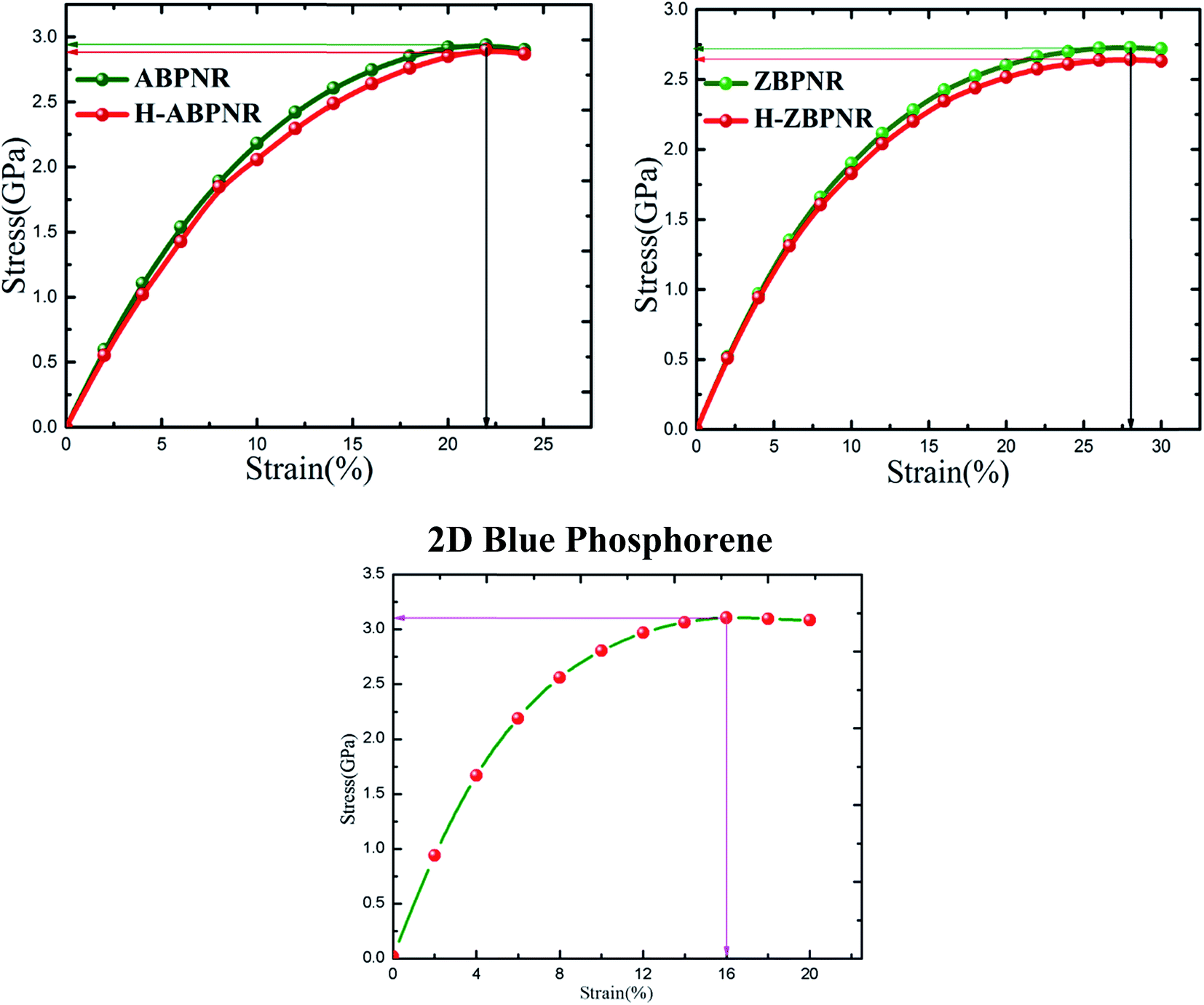 | ||
| Fig. 4 Strain versus stress curves of bare and hydrogen passivated edge structure of blue phosphorene nanoribbons for width n = 12. The horizontal and vertical lines with arrow indicate the tensile strength and ultimate tensile strain of nanoribbons. Strain–stress curve for 2D blue phosphorene has also been given for comparison. | ||
Thereafter, keeping in view the critical value of strain, we investigated the evolution of electronic structure of BPNRs on the function of strain. It is found that the electronic band gap of considered ribbons decreases continuously with increasing strain, eventually, rendering them nearly metallic at a critical value (Fig. 5). On carefully looking at the evolution of electronic structure with strain, the valance band maximum (VBM) and conduction band minimum (CBM) systematically shifts towards Fermi level which tends to close the band gap at Γ-point. At ultimate tensile strain, the semiconductor-to-metal transition occurs for bare ZBPNR while few meV band gap remains intact for other ribbons (Fig. 5). These changes in electronic structure are attributed to the redistribution of atomic orbitals on the application of applied strain.
 | ||
| Fig. 5 (a and b) Variation in band gap with applied strain for bare and hydrogen passivated edges of blue phosphorene nanoribbons for width n = 12. (c–f) Electronic band structures at different strain values are also shown. | ||
In order to get deep insight into the change in electronic structure with applied strain, we calculate the orbital resolved partial density of states (PDOS) of unstrained and strained BPNRs (Fig. 6). It is important to note that on the application of in-plane strain, the out-of-plane orbitals get redistributed in significant manner while in-plane orbitals remain nearly unaffected. The pz orbitals of phosphorous atom of strained BPNRs shift towards Fermi energy that lead to change in electronic band gap. The shift of pz orbitals towards Fermi energy in more pronounced for higher strain which results into semiconductor-to-metal transitions in BPNRs at critical value of strain (Fig. 6).
 | ||
| Fig. 6 Orbital resolved partial density of states of in-plan (px and py) and out-of-plan (pz) orbitals of phosphorous atoms of strain-free and strained BPNRs. | ||
3.3 Dielectric properties of BPNRs
We now investigate the effect of width and mechanical strain on the dielectric properties of BPNRs. The static dielectric constant (εs) was obtained by calculating the value of real part of dielectric function (ε1) at zero frequency. The calculated εs as a function of width of both ABPNR and ZBPNR show oscillatory behaviour (Fig. 7a). On careful examination we found that the change in εs with varying width shows its link with the change in electronic band gap (Eg) on the same width e.g. for ABPNR at n = 8, Eg ∼ 0 (minimum) while corresponding εs is found to be ∼4.5 (maximum); the maximum Eg in ABPNR is calculated as ∼3 eV at n = 3 while the εs is calculated minimum (∼1.9) at the same width; for ZBPNR, the Eg remains constant at n = 6–9 (Eg ∼ 0.5 eV) and the corresponding εs is calculated as ∼3.5–3.7 at the same widths. This type of behaviour of Eg and εs may be attributed to the Penn's model expression,45 where electronic band gap of the semiconductor is roughly related with the static dielectric constant (εs) as , where ωP is plasmonic frequency.
 | ||
| Fig. 7 Static dielectric constant (εs) versus width (n) for (a) bare and (b) edge passivated BPNRs. εs as a function of strain for (c) ABPNRs and (d) ZBPNRs are give at width n = 12. | ||
In case of H-ABPNR and H-ZBPNR, Eg systematically decreases as a function of width (Fig. 3d) while corresponding εs at same widths shows inverse trend with fluctuations at higher widths (Fig. 7b) which may be attributed to the pronounced effect of distinctly different plasmonic excitations at wider width ribbons. εs is also found to change with applied strain (Fig. 7c and d) which shows nearly inverse trend as compared to Eg with strain (Fig. 5a and b). At the critical value of strain, εs for ABPNR, H-ABPNR, ZBPNR and H-ZBPNR is calculated as 16.2, 15.1, 9.8 and 5.5 respectively. Higher value of εs indicate metallic or nearly metallic character of these ribbons.
Now we investigate the change in imaginary part of dielectric function (ε2) and electron energy loss spectra (EELS) as a function of width. It is noticeable that ε2 in passivated BPNRs possess structure peak at ∼5 eV while additional structure at ∼1 eV is found for bare BPNRs (Fig. 8). We attribute the additional structure in bare BPNRs to the interband transitions between the dangling bond states near Fermi energy which disappear in H-BPNRs. The energy of structure peaks of ε2 remains independent of width while the intensity of wider width BPNRs is at higher magnitude. The higher intensity of wider BPNRs is due to the increased number of allowed bands available for interband transitions.
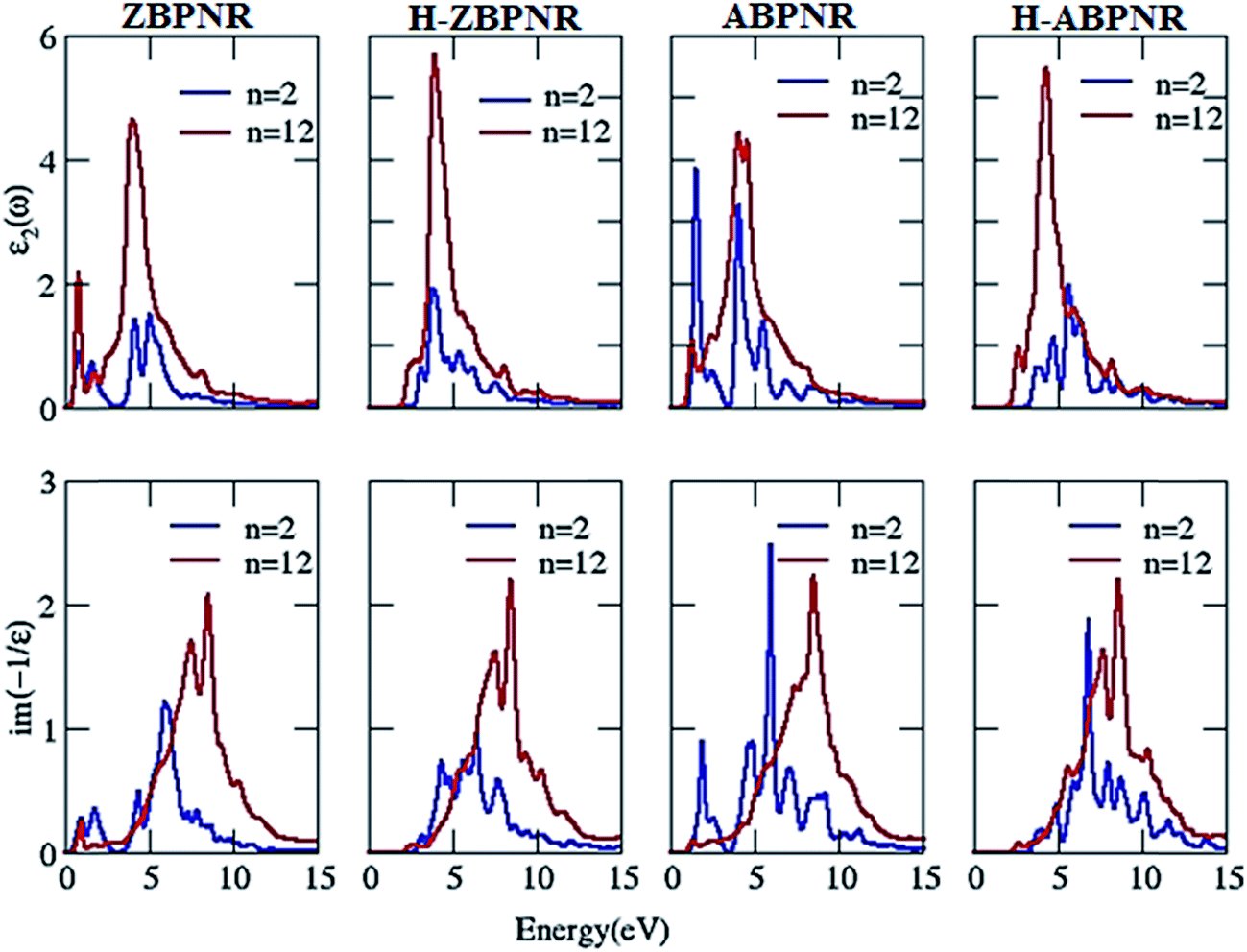 | ||
| Fig. 8 Imaginary part of dielectric function (ε2) and electron energy loss spectra (EELS) at n = 2 and n = 12 for bare and hydrogen passivated edges of blue phosphorene nanoribbons. | ||
The structure peaks in electron energy loss spectra (EELS) spectra give the collective excitation of electron which is known as plasmons. Low energy plasmons are called π-plasmons which are associated with the excitation of weak π-electrons while high energy plasmons are π + σ plasmons which are associated with both weak π and strong σ electrons.46,47 EELS show two plasmonic features for bare BPNRs, one at low energy <5 eV and second at higher energy >5 eV, while H-BPNRs have been found to exhibit plasmonic excitations only at higher energy (>5 eV) (Fig. 8). The low energy plasmonic features (<5 eV) are due to π-electrons while the higher energy (>5 eV) plasmonic features comes from both π- and σ-electrons of BPNRs. Interestingly, plasmonic energy gets blue shifted as we go from width n = 2 to n = 12 (Fig. 8). The blue shift in the plasmonic energy is calculated as large as ∼3 eV (Table T1 of ESI†). This much amount of plasmonic energy difference makes electron energy loss spectroscopy useful in order to identify the width of BPNRs in real experimental situation.
Next we consider the effect of mechanical strain on ε2 and EELS of BPNRs. The uniaxial strain induces small red shift in ε2 of all the considered BPNRs (Fig. 9), which is attributed to the modification in electronic band dispersion due to superposition of atomic orbitals on the application of applied strain. Similarly, EELS of BPNRs is also found to be red shifted on the application of strain. The red shift in EELS is more pronounced in π + σ plasmonic structures (Fig. 9) where as large as ∼2 eV shift is calculated in plasmonic energy (Table T1 of ESI†). These tunable dielectric properties of BPNRs with width and external strain may have importance in optoelectronic devices based on BPNRs.
 | ||
| Fig. 9 Imaginary part of dielectric function (ε2) and electron energy loss spectra (EELS) at 2% and ultimate tensile strain for bare and hydrogen passivated edges of blue phosphorene nanoribbons. | ||
4. Summary
In summary, we have performed a detailed first principles study of optoelectronic properties of ultra-narrow BPNRs. The electronic band gap of BPNRs is found to be width and edge-specific. The ultimate tensile strength of BPNRs is calculated as ∼3 GPa with critical strain value >20%. BPNRs are found to possess nearly metallic characteristics at critical value of strain which is consistent with the higher value of calculated static dielectric constant. ε2 for passivated BPNRs possess structure peak at ∼5 eV while additional structure at ∼1 eV is found for bare BPNRs which is attributed to the interband transitions between the dangling bond states near the Fermi energy. Interestingly, plasmonic energy gets blue shifted on increasing the width of BPNRs while it shows red-shift on the application of longitudinal tensile strain. These tunable electronic and dielectric properties of BPNRs may be useful for the optoelectronic applications.Acknowledgements
AK gratefully acknowledge the UGC/MHRD, Govt. of India, New Delhi for startup grant. RS is grateful to the Central University of Punjab for financial assistance. We acknowledge the computational facilities provided by CUPB to carry out this work.References
- K. Novoselov, D. Jiang, F. Schedin, T. Booth, V. Khotkevich, S. Morozov and A. Geim, Two-dimensional atomic crystals, Proc. Natl. Acad. Sci. U. S. A., 2005, 102, 10451 CrossRef CAS PubMed.
- A. K. Geim and K. S. Novoselov, The rise of graphene, Nat. Mater., 2007, 6, 183 CrossRef CAS PubMed.
- S. Z. Butler, S. M. Hollen, L. Cao, Y. Cui, J. A. Gupta, H. R. Gutiérrez and E. Johnston-Halperin, Progress, challenges, and opportunities in two-dimensional materials beyond graphene, ACS Nano, 2013, 7, 2898–2926 CrossRef CAS PubMed.
- T. Palacios, A. Hsu and H. Wang, Applications of graphene devices in RF communications, IEEE Comm. Mag., 2010, 48, 122–128 CrossRef.
- A. Kara, H. Enriquez, A. P. Seitsonen, L. L. Y. Voon, S. Vizzini, B. Aufray and H. Oughaddou, A review on silicene—new candidate for electronics, Surf. Sci. Rep., 2012, 67, 1–18 CrossRef CAS.
- B. Mohan, A. Kumar and P. K. Ahluwalia, A first principle calculation of electronic and dielectric properties of electrically gated low-buckled mono and bilayer silicene, Phys. E, 2013, 53, 233–239 CrossRef CAS.
- P. Jamdagni, A. Kumar, A. Thakur, R. Pandey and P. K. Ahluwalia, Stability and electronic properties of SiGe-based 2D layered structures, Mater. Res. Express, 2015, 2, 016301 CrossRef.
- D. Jariwala, V. K. Sangwan, L. J. Lauhon, T. J. Marks and M. C. Hersam, Emerging device applications for semiconducting two-dimensional transition metal dichalcogenides, ACS Nano, 2014, 8, 1102–1120 CrossRef CAS PubMed.
- A. Kumar and P. K. Ahluwalia, Electronic transport and dielectric properties of low dimensional structures of layered transition metal dichalcogenides, J. Alloys Compd., 2014, 587, 459–467 CrossRef CAS.
- A. Kumar, H. He, R. Pandey, P. K. Ahluwalia and K. Tankeshwar, Pressure and electric field induced metallization in the phase-engineered ZrX2 (X = S, Se, Te) bilayers, Phys. Chem. Chem. Phys., 2015, 17, 19215 RSC.
- P. Jamdagni, A. Kumar, M. Sharma, A. Thakur and P. K. Ahluwalia, Electronic properties and STM images of vacancy clusters and chains in functionalized silicene and germanene, Phys. E, 2017, 85, 65–73 CrossRef CAS.
- L. Kou, C. Chen and S. C. Smith, Phosphorene: fabrication, properties, and applications, J. Phys. Chem. Lett., 2015, 6, 2794–2805 CrossRef CAS PubMed.
- A. Castellanos-Gomez, L. Vicarelli, E. Prada, J. O. Island, K. L. Narasimha-Acharya, S. I. Blanter, D. J. Groenendijk, M. Buscema, G. A. Steele, J. V. Alvarez, H. W. Zandbergen, J. J. Palacios and H. S. J. van der Zant, Isolation and characterization of few-layer black phosphorus, 2D Materials., 2014, 1, 025001 CrossRef.
- H. Liu, A. T. Neal, Z. Zhu, Z. Luo, X. Xu, D. Tománek and P. D. Ye, Phosphorene: an unexplored 2D semiconductor with a high hole mobility, ACS Nano, 2014, 8, 4033–4041 CrossRef CAS PubMed.
- L. Li, Y. Yu, G. N. Ye, Q. Ge, X. Ou, H. Wu, D. Feng, X. H. Chen and Y. Zhang, Black phosphorous filed effect transistors, Nat. Nanotechnol., 2014, 9, 372–377 CrossRef CAS PubMed.
- Y. Cai, G. Zhang and Y. W. Zhang, Layer-dependent band alignment and work function of few-layer phosphorene, Sci. Rep., 2014, 4, 6677 CrossRef CAS PubMed.
- J. Guan, Z. Zhu and D. Tomanek, Phase coexistence and metal-insulator transition in few-layer phosphorene: a computational study, Phys. Rev. Lett., 2014, 113, 046804 CrossRef PubMed.
- Z. Zhu and D. Tománek, Semiconducting layered blue phosphorus: a computational study, Phys. Rev. Lett., 2014, 112, 176802 CrossRef PubMed.
- S. Kaur, A. Kumar, S. Srivastava and K. Tankeshwar, Electronic structure engineering of various structural phases of phosphorene, Phys. Chem. Chem. Phys., 2016, 18, 18312–18322 RSC.
- G. Wang, G. C. Loh, R. Pandey and S. P. Karna, Out-of-plan structural flexibility of phosphorene, Nanotechnology, 2016, 27, 055701 CrossRef PubMed.
- K. Jimin, S. B. Seung, H. R. Sae, S. Yeongsup, P. Soohyung, P. Byeong, D. Jonathan, Y. Yeonjin, J. C. Hyoung and S. K. Keun, Observation of tunable band gap and anisotropic Dirac semimetal state in black phosphorous, Science, 2015, 349, 723 CrossRef PubMed.
- J. Cai, P. Ruffieux, R. Jaafar, M. Bieri, T. Braun, S. Blankenburg, M. Muoth, A. P. Seitsonen, M. Saleh, X. Feng, K. Mullen and R. Fasel, Atomically precise bottom-up fabrication of graphene nanoribbons, Nature, 2010, 466, 470–473 CrossRef CAS PubMed.
- J. Bai, X. Duan and Y. Huang, Rational fabrication of graphene nanoribbons using a nanowire etch mask, Nano Lett., 2009, 9, 2083–2087 CrossRef CAS PubMed.
- L. Jiao, X. Wang, G. Diankov, H. Wang and H. Dai, Facile synthesis of high-quality graphene nanoribbons, Nat. Nanotechnol., 2010, 5, 321–325 CrossRef CAS PubMed.
- S. Masubuchi, M. Ono, K. Yoshida, K. Hirakawa and T. Machida, Fabrication of graphene nanoribbon by local anodic oxidation lithography using atomic force microscope, Appl. Phys. Lett., 2009, 94, 082107 CrossRef.
- V. Tran and L. Yang, Scaling laws for the band gap and optical response of phosphorene nanoribbons, Phys. Rev. B: Condens. Matter Mater. Phys., 2014, 89, 245407 CrossRef.
- J. Xie, M. S. Si, D. Z. Yang, Z. Y. Zhang and D. S. Xue, A theoretical study of blue phosphorene nanoribbons based on first principles calculations, J. Appl. Phys., 2014, 116, 073704 CrossRef.
- A. Ramasubramaniam and A. R. Muniz, Ab initio studies of thermodynamic and electronic properties of phosphorene nanoribbons, Phys. Rev. B: Condens. Matter Mater. Phys., 2014, 90, 085424 CrossRef.
- W. Li, G. Zhang and Y. W. Zhang, Electronic properties of edge-hydrogenated phosphorene nanoribbons: a first-principles study, J. Phys. Chem. C, 2014, 118, 22368–22372 CAS.
- T. Hu and J. Hong, Electronic structure and magnetic properties of blue phosphorene nanoribbons, J. Appl. Phys., 2015, 118, 054301 CrossRef.
- X. Han, H. Morgan Stewart, S. A. Shevlin, C. R. A. Catlow and Z. X. Guo, Strain and orientation modulated bandgaps and effective masses of phosphorene nanoribbons, Nano Lett., 2014, 14, 4607–4614 CrossRef CAS PubMed.
- Y. Li, S. Yang and J. Li, Modulation of the electronic properties of ultrathin black phosphorus by strain and electrical field, J. Phys. Chem. C, 2014, 118, 23970–23976 CAS.
- A. Kimouche, M. M. Ervasti, R. Drost, S. Halonen, A. Harju, P. M. Joensuu and P. Liljeroth, Ultra-narrow metallic armchair graphene nanoribbons, Nat. Commun., 2015, 6, 10177 CrossRef CAS PubMed.
- H. Shen, A. Cresti, W. Escoffier, Y. Shi, X. Wang and B. Raquet, Peculiar magneto transport features of ultranarrow graphene nanoribbons under high magnetic field, ACS Nano, 2016, 10, 1853–1858 CrossRef CAS PubMed.
- J. M. Soler, E. Artacho, J. D. Gale, A. García, J. Junquera, P. Ordejón and D. Sánchez-Portal, The SIESTA method for ab initio order-N materials simulation, J. Phys.: Condens. Matter, 2002, 14, 2745 CrossRef CAS.
- W. Kohn, A. D. Becke and R. G. Parr, Density functional theory of electronic structure, J. Phys. Chem., 1996, 100, 12974–12980 CrossRef CAS.
- W. Kohn, Nobel Lecture: Electronic structure of matter—wave functions and density functionals, Rev. Mod. Phys., 1999, 71, 1253 CrossRef CAS.
- N. Troullier and J. L. Martins, Efficient Pseudopotentials for Plane-Wave Calculations, Phys. Rev. B: Condens. Matter Mater. Phys., 1993, 43, 1991 Search PubMed.
- J. P. Perdew, K. Burke and Y. Wang, Erratum: Generalized gradient approximation for the exchange-correlation hole of a many-electron system, Phys. Rev. B: Condens. Matter Mater. Phys., 1996, 54, 16533 CrossRef CAS.
- S. S. Yu, Q. B. Wen, W. T. Zheng and Q. Jiang, Electronic properties of graphene nanoribbons with armchair-shaped edges, Mol. Simul., 2008, 34, 1085–1090 CrossRef CAS.
- B. Zhou, B. Zhou, Y. Zeng, G. Zhou and M. Duan, Tunable electronic and transport properties for ultranarrow armchair-edge silicene nanoribbons under spin–orbit coupling and perpendicular electric field, Phys. Lett. A, 2016, 380, 282–287 CrossRef CAS.
- P. Koskinen, S. Malola and H. Hakkinen, Self-Passivating Edge Reconstructions of Graphene, Phys. Rev. Lett., 2008, 101, 115502 CrossRef PubMed.
- G. Gao, X. Liu, G. Zhang and Y.-W. Zhang, Nanotube-Terminated Zigzag Edge of Phosphorene formed by Self-Rolling Reconstruction, Nanoscale, 2016, 8, 17940–17946 RSC.
- D. Cao, T. Shen, P. Liang, X. Chen and H. Shu, Role of Chemical Potential in Flake Shape and Edge Properties of Monolayer MoS2, J. Phys. Chem. C, 2015, 119, 4294–4301 CAS.
- D. R. Penn, Wave-number-dependent dielectric function of semiconductors, Phys. Rev., 1962, 128, 2093 CrossRef CAS.
- O. V. Sedelnikova, L. G. Bulusheva and A. V. Okotrub, Ab initio study of dielectric response of rippled graphene, J. Chem. Phys., 2011, 134, 244707 CrossRef CAS PubMed.
- A. Kumar and P. K. Ahluwalia, Effect of quantum Confinement on electronic and dielectric properties of niobium dichalcogenides NbX2 (X = S, Se, Te), J. Alloys Compd., 2013, 550, 283–291 CrossRef CAS.
Footnote |
| † Electronic supplementary information (ESI) available. See DOI: 10.1039/c6ra26253h |
| This journal is © The Royal Society of Chemistry 2017 |