
 Open Access Article
 This Open Access Article is licensed under a
 Creative Commons Attribution 3.0 Unported Licence
Efficient non-halogenated solvent for the template-free solution synthesis of ultralong copper octaethylporphyrin nanowire networks with strong photoswitching properties†
Jia-Jia Liab,
Hong-Dan Peng*b,
Li-Yi Shia,
Hao-Di Wub and
Ge-Bo Pan *b
*b
aDepartment of Chemistry, College of Sciences, Shanghai University, 200444 Shanghai, P. R. China
bSuzhou Institute of Nano-tech and Nano-bionics, Chinese Academy of Sciences, 215123 Suzhou, P. R. China. E-mail: hdpeng2012@sinano.ac.cn; gbpan2008@sinano.ac.cn; Fax: +86-512-62872663
First published on 23rd January 2017
Abstract
Rationally solution-processed organic electronics are expected to pave the way for low-cost and large-area devices with new and exciting applications. In this study, a non-halogenated solvent was employed for the first time for the one-step and scalable synthesis of extremely high aspect ratio organic semiconducting nanowires of copper octaethylporphyrin (CuOEP) using a cast assembly method under a solvent atmosphere. Remarkably, these single crystalline nanowires exhibited excellent photoswitching effects with reliable reproducibility and superior stability, indicating their potential for application in high-performance optoelectronic devices.
In recent years, solution-processed organic optoelectronic nanodevices have attracted increasing interest because of their good compatibility with solution-based low temperature processing methods that have unlocked the potential for low-cost and high-throughput fabrication over large areas on flexible substrates.1,2 By skillfully harnessing the supramolecular forces that govern the interactions between organic semiconductors molecules, nanoscale aggregation can be directed to induce the formation of molecular assemblies with long-range order.3 In particular, the molecular packing in highly organized one-dimensional (1D) nanostructured semiconductors with large surface-to-volume ratios facilitates directional carrier transport and exciton diffusion to effectively enhance the performance of the corresponding devices.4 Compared to short nanorods or nanobelts, millimeter-long organic nanowires are especially desirable on the basis of their many advantages including reliable and convenient manipulation, decreased junction resistance and a greater possibility to realize new applications. However, controlling the anisotropic aggregation of small organic molecules when constructing ultralong single crystalline 1D micro/nanowires has been proven to be a challenging task due to the complex intermolecular interactions and rigorous conditions required for single crystal growth.
Photodetectors as binary switches are indispensable elements in imaging techniques, and lightwave optical communications, as well as in future memory storage and optoelectronic circuits.5 Until now, most of the previous studies have focused on photodetection using inorganic individual nanostructure-based devices.6 These devices normally suffer from complex and high cost lithographic processing and exhibit large variations in performance. Alternatively, the emerging inorganic nanowire network devices based on a large number of simultaneously operating nanostructures7,8 reveal better detector characteristics and can be fabricated using cost effective methods over large areas. However, in contrast, the same research is much less advanced for their organic counterparts, although they possess the great inherent advantages of conformal flexibility and the simplicity of designing molecules to tune their electronic properties. In addition, many reported organic detectors exhibit low switch ratios and relatively long response times/decay times, which have seriously limited their practical applications.9–11 Thus, it is imperative to investigate the preparation of organic nanowire networks for the development of high performance photoswitches.
Metalloporphyrins possess many desirable structural and functional properties and are a favorite building block for the construction of 1D nanostructures.12 In nature, assemblies of porphyrin derivatives are exploited by photosynthesising plants and organisms for their light-harvesting capabilities. The rapid growth of environmental pollution problems has prompted the quest for the development of cleaner solution-based processing techniques for porphyrin self-assembly. However, porphyrin chloroform solutions and different types of templates were still predominant prerequisites in the previously reported methods,13–15 and chloroform is highly detrimental to the environment and human health and unfavorable for large-scale production.16 Meanwhile, the rather tedious post-synthesis process of eliminating templates has the risk of destroying the desired structure.
Herein, as a proof-of-concept, we report for the first time the successful fabrication of ultralong CuOEP nanowires with a very high aspect ratio through a facile one-step method without using any template directing agents. In fact, evaporation induced self-assembly using non-halogenated solvents can offer an economical and scalable route to well-defined 1D crystalline porphyrin nanosystems, for instance m-xylene has low toxicity and is easier to remove to prevent its environmental accumulation.17 Furthermore, the as-constructed prototype network photodetector based on these nanowires showed fast, reversible and stable photo-response characteristics. Specifically, the photoswitching ratios were up to over 5000, which is significantly increased by about two orders of magnitude when compared to that based on reported short CuOEP nanorods.18 As far as we know, this is one of the highest switch ratios for small molecular nanowire-based photoswitches.
Given that water is a cheap and safe solvent and CuOEP is not water soluble, a simple reprecipitation method without surfactant was attempted to prepare the nanowires. Unfortunately, although the toxic halogenated solvent was replaced, very short nanorods of CuOEP (about 150 nm in length with a low aspect ratio of <10) were obtained.18 The large difference in CuOEP solubility in good solvents and water leads to the rapid formation of unwanted (route-dependent) kinetic aggregates rather than thermodynamically optimized structures, resulting in reproducibility issues and suboptimal performance. CuOEP is a macrocyclic molecular building block that is sterically unencumbered (Fig. S1†). All four pyrrole-ring moieties of each planar CuOEP molecule simultaneously have strong π–π interactions with their neighbors along the three crystallographic directions. In this study, we have developed a facile process to fabricate single-crystalline ultralong nanowires of CuOEP by utilizing self-assembly at the solution–substrate interface upon solution evaporation. In a typical experiment, 40 μL of CuOEP m-xylene solution (∼1 mg mL−1) was injected onto substrates of heavily-doped Si, which were then placed in a 100 mL closed beaker containing 10 mL of m-xylene. During the whole procedure, a solvent atmosphere was created and the evaporation speed of the solvent (i.e. the saturation degree of the solution) could be well controlled. Such a self-assembly approach allowed the CuOEP molecules sufficient time to adjust themselves and arrange in a way that was favorable for stacking in a highly ordered manner. After solvent evaporation, the well-defined CuOEP nanowires were formed (Fig. S2†). To remove the solvent thoroughly, the nanowires were post-annealed at 150 °C for 45 min. Interestingly, the self-assembly of the CuOEP nanowires exhibited no obvious substrate dependence. Regardless of whether the substrate used was glass, quartz wafers, or flexible polyethylene terephthalate (PET), beautiful nanowires were always obtained (Fig. S3†). Moreover, varying the concentration of the CuOEP solution provides the opportunity to change the density of the nanowire networks, but with little influence on the diameter of the nanowires (Fig. S4†).
Due to the good solubility of CuOEP molecules in chloroform, tetrahydrofuran (THF), anisole, etc. they have also been used as the solvent, as exemplified in Fig. S5,† and the results revealed that m-xylene was the optimal choice of solvent for the preparation of the desired CuOEP nanowire crystals. On the one hand, it has good volatility and produces a high solvent vapor pressure in the upper space of the beaker under evaporation conditions. On the other hand, it is a non-coordinating solvent. In good contrast, there are additional axial Cu–O coordination interactions between the solvent anisole and the copper center of the CuOEP molecules. The solvent–porphyrin molecular interactions could counterbalance the intermolecular interactions, particularly the hydrophobic interactions between the side chains, and in-turn exert significant influence on the molecular packing modes in the aggregates. Thus, during crystallization under anisole solution evaporation conditions, CuOEP tends to not only π-stack, but also stack in a manner lateral to the aromatic core, which produces irregular plate or needle-shaped bulk crystals rather than nanowires. The unique weak substrate dependence and strong solvent dependence would be meaningful for the controllable assembly of these conjugated CuOEP nanowires and the further extension of their potential applications in devices.
The morphology of the obtained CuOEP nanowires was examined by scanning electron microscopy (SEM), atomic force microscopy (AFM) and transmission electron microscopy (TEM), as depicted in Fig. 1a, c and d. It can be clearly observed that the assembled products have a high morphological purity, very uniform diameter and smooth surface throughout their length. The nanowires have an average diameter ranging from 150 to 500 nm, and average lengths of up to 850 μm. A maximum aspect ratio of ∼2300 can be obtained. Furthermore, the CuOEP nanowires are highly fluorescent, emitting intense red light when excited with blue light (Fig. 1b). The internal crystalline structure of the CuOEP nanowires was investigated using X-ray diffraction (XRD). All the diffraction peaks could be well-indexed to a triclinic phase.19 The lattice constants are a = 13.314 Å, b = 13.392 Å, c = 4.805 Å, α = 92.42°, β = 93.38°, and γ = 113.08°. Moreover, the diffraction peak of the (1![[1 with combining macron]](https://www.rsc.org/images/entities/char_0031_0304.gif) 0) plane of the nanowires corresponding to the 2θ = 7.96° is significantly enhanced relative to that in the simulated pattern, revealing that their preferential growth was along the [001] orientation (Fig. 1e and S6†). This was further confirmed by the well-defined selected-area electron diffraction (SAED) pattern of a single CuOEP nanowire. The [10] Miller plane of the CuOEP nanowire was normal to the electron beam, consistent with the [10] intense peak in the powder XRD pattern. In addition, the smooth nanowire had a single crystalline morphology and the wire axis is the c axis of the crystal, which can eliminate the effects of grain boundaries for the fabrication of high-quality devices. The energy dispersive X-ray spectroscopy (EDX) spectrum of the nanowire unambiguously suggested the presence of Cu and N (Fig. 1f).
0) plane of the nanowires corresponding to the 2θ = 7.96° is significantly enhanced relative to that in the simulated pattern, revealing that their preferential growth was along the [001] orientation (Fig. 1e and S6†). This was further confirmed by the well-defined selected-area electron diffraction (SAED) pattern of a single CuOEP nanowire. The [10] Miller plane of the CuOEP nanowire was normal to the electron beam, consistent with the [10] intense peak in the powder XRD pattern. In addition, the smooth nanowire had a single crystalline morphology and the wire axis is the c axis of the crystal, which can eliminate the effects of grain boundaries for the fabrication of high-quality devices. The energy dispersive X-ray spectroscopy (EDX) spectrum of the nanowire unambiguously suggested the presence of Cu and N (Fig. 1f).
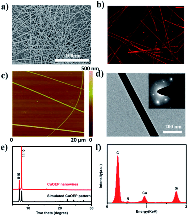 | ||
| Fig. 1 (a) The typical SEM image of the self-assembled 1D CuOEP nanowires; (b) a confocal fluorescence microscopy image of the CuOEP nanowires; (c) AFM and (d) TEM images of a CuOEP nanowire. The inset is the corresponding SAED pattern of the CuOEP nanowire; (e) the XRD pattern of the CuOEP nanowires and the simulated pattern from single crystal data; (f) the EDX spectrum of the CuOEP nanowires. | ||
As shown in Fig. 2a, the FT-IR spectrum of the nanowires has similar features to that of the source powder CuOEP. The four metal-sensitive characteristic bands are observed at 749, 916, 986 and 1221 cm−1, implying that the CuOEP molecules do not undergo any decomposition or other chemical reactions during the solvent evaporation process.20,21 Fig. 2b shows the typical UV-vis absorption spectra of nanowires deposited on quartz and CuOEP monomers in m-xylene solution. Similar to the monomers, the nanowires also have three characteristic adsorption bands, labelled S, Q1 and Q2. However, compared to the sharp peaks from the monomers, the bands of the nanowires are substantially broadened. Moreover, the Q bands are red-shifted, whereas the S band is blue-shifted. These changes are associated with the effects of highly ordered molecular packing in the CuOEP nanowires and H-aggregation formation.22 From the UV-vis spectra, the optical energy gap of the CuOEP nanowires is roughly estimated to be 2.0 eV (Fig. S7†) by means of the classical Tauc approach.23 This value is narrow enough to permit the generation of a substantial number of charge carriers by white light irradiation.
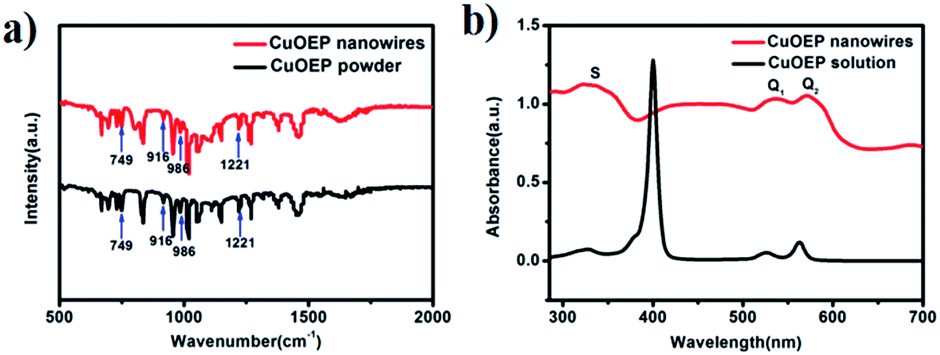 | ||
| Fig. 2 (a) FTIR spectra of the nanowires and the source powder CuOEP; (b) UV-vis absorption spectra of the CuOEP nanowires on a quartz substrate and CuOEP monomers in m-xylene solution. | ||
The photoresponse properties were investigated by fabrication of a prototype photoelectric device based on an interconnected network of ultralong CuOEP nanowires, which is beneficial for rapid long-range charge transport via effective intermolecular π-electron delocalization. Fig. 3a and b show a schematic illustration and a typical SEM image of the as-constructed device, respectively. It is clear that the randomly oriented and entangled CuOEP nanowires have connected the two pre-patterned Au electrodes. Fig. 3c shows the current (I)–voltage (V) curves of the device in the dark and under continuous white light illumination at different light intensities. As the voltage increases, the photocurrent under light illumination is markedly higher than that obtained in the dark. At a bias of 20 V, the nanowire network in the dark shows a relatively low current of 0.27 pA. However, a high current of about 315 pA is obtained even at a low power density of 1.57 mW cm−2. This corresponds to a photocurrent on/off ratio of ca. 1164. As expected, by increasing the power density, this value can be further raised, which can be attributed to a change in the photo-generated carriers at different light densities. At a higher power density of 12.05 mW cm−2, the photocurrent on/off ratio can reach 5412. To the best of our knowledge, this value is much higher than that of other organic semiconductors.24–27 We also fabricated photoswitches based on short CuOEP nanorods for comparison, however, these devices displayed extremely low switch ratios (about several to tens). This is probably because the large surface-to-volume ratio of the ultralong CuOEP nanowires greatly increases the number of surface trap states, and facilitates oxygen adsorption/desorption at the surface. Fig. S8† shows the relationship between the photocurrent and incident light power densities. This can be well fitted with a simple power law I–Pθ, where the exponent θ determines the response of the photocurrent to the light intensity. The fitting demonstrates a power dependence of ∼0.59 at 10 V, ∼0.68 at 20 V, and ∼0.65 at 30 V. The nearly identical θ value for different bias voltages indicates that the response to light intensity is voltage-independent. Similar results could be observed in CdS nanoribbons or mixed perovskite nanofibers.28,29 The non-unity exponent (0.5 < θ < 1) is mainly attributed to complex processes within the semiconductor under light illumination, including electron–hole generation, trapping, and recombination.30 These above characteristics suggest the excellent photo-capture properties of the device.
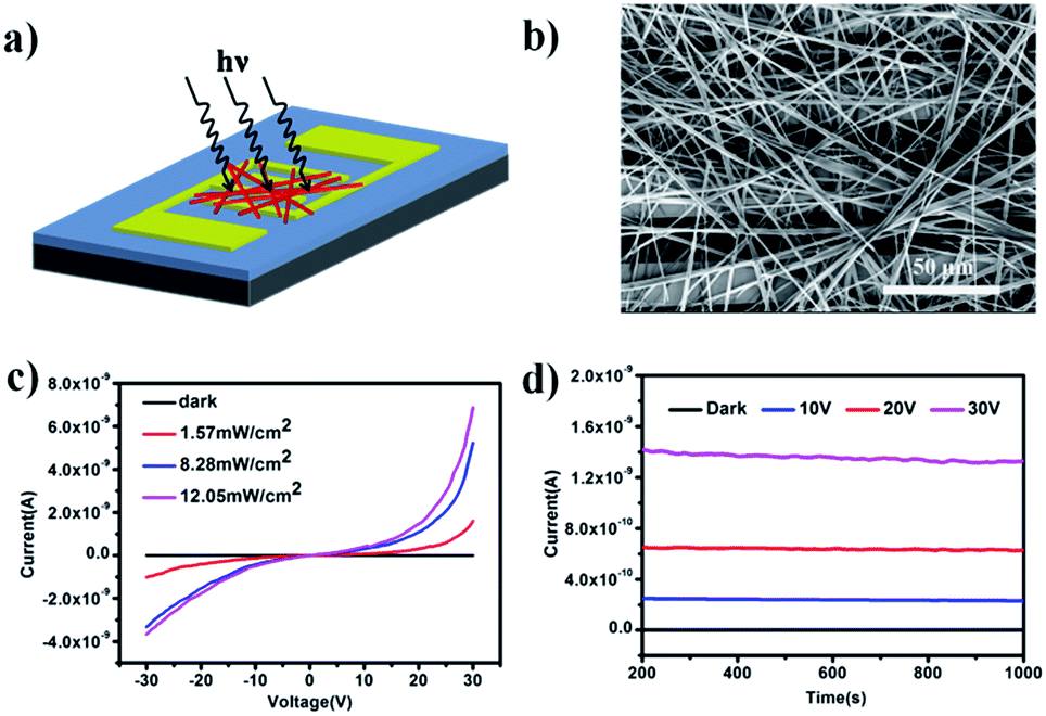 | ||
| Fig. 3 (a) A schematic illustration and (b) an SEM image of the prepared prototype device of the CuOEP nanowire network. (c) I–V curves of the CuOEP nanowire network in the dark and under light illumination at different incident power densities. (d) The current versus time over a continuous 800 s in the dark and under illumination. | ||
Moreover, photoconduction switching was demonstrated to be prompt and reversible by turning a light on and off under an illumination intensity of 12.05 mW cm−2 (Fig. S9a†). It can be seen that the current of the devices increases with the bias voltage and shows two distinct states, a “low” current state in the dark and a “high” current state under white light illumination. All these devices exhibited excellent reproducibility and stability without serious attenuation after eleven cycles of on/off operation. The response speed is a key parameter which determines the capability of a photodetector to follow a fast-varying optical signal. From the enlarged view (Fig. S9b†) of one of the on–off cycles, the rise and decay times (defined as the time required to reach 90% of the final equilibrium value) were estimated to be about 0.6 s and 0.8 s, respectively, which demonstrates that the devices show a faster response time compared with other nanostructure-based photoswitches.31 In addition, the devices also show high photo-current durability and environmental stability. As shown in Fig. 3d, after 800 s of illumination, the current in the dark remains almost constant, while the photocurrent also holds nearly steady even under a light intensity of 12.05 mW cm−2 with an applied voltage 30 V and only decreases by 1.6% by the end of the cycle. This deviation is negligibly small, which might be due to unavoidable light induced degradation of the material.
Different from traditional organic photodetectors with the presence of good ohmic contacts at the semiconductor/electrode interface, nonlinear I–V curves were typically observed for the network devices in the present work (Fig. 3c), indicating a unique barrier dominated conducting mechanism.33 Because CuOEP is a p-type semiconductor, we assume that the carrier traps are mainly distributed near the HOMO level. As can be seen in the Fig. 4a, the HOMO of CuOEP (5.1 eV) matches well with the Fermi energy level of Au (5.2 eV). Thus, the hole’s injection could occur relatively easily from the Au source electrode to the CuOEP crystal. On the other hand, the CuOEP nanowire–nanowire (NW–NW) junction barrier is analogous to two back to back Schottky barriers. As illustrated in Fig. 4b, upon illumination, the photogenerated electron–hole pairs in the reverse-biased Schottky interface region are separated by the built-in electron field, resulting in an increase in the free carrier density. Meanwhile, the NW–NW barrier height is lowered due to a thinning of the shell depletion layer of the CuOEP nanowires. Compared with the surface dominated oxygen-diffusion process for ordinary ohmic-type photodetectors, this light-induced barrier modulation is much faster. Thus, the key formation of Schottky junctions in these network devices can effectively facilitate charge separation/transport and reduce electron–hole recombination rates, which contribute to significant performance improvement.
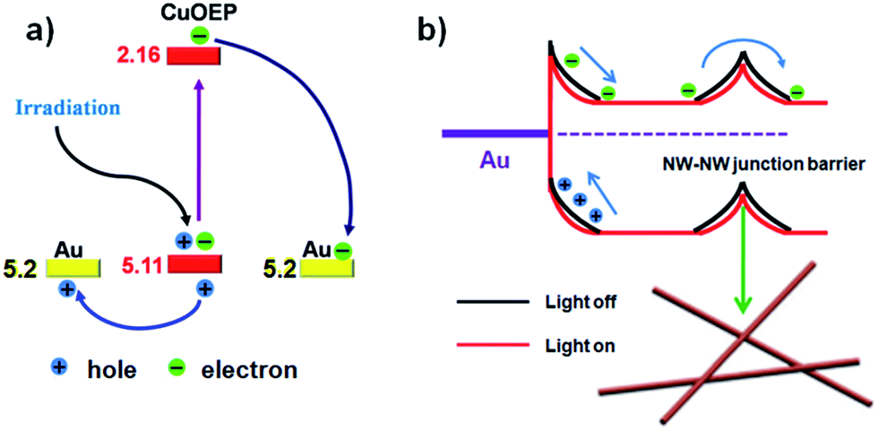 | ||
| Fig. 4 (a) Energy band diagram at the interface of the CuOEP nanowire and the Au contact and charge separation under light irradiation; the HOMO and LUMO levels of the CuOEP molecule were obtained by means of density functional theory (DFT) calculations.32 (b) Schematic illustration of the Schottky barrier and NW–NW junction barrier for charge transfer in the network devices. The bending bands are used to represent the electron depletion/hole accumulation layers (response to incident light), which originate from the surface charge/adsorbates. | ||
In summary, evaporation of a CuOEP solution under a solvent atmosphere is in principle a non-equilibrium and complex process. An appropriate self-assembly approach and the solvent conditions play a crucial role in determining the morphology of the obtained CuOEP aggregates and the functionality of the final devices. Ultralong and high-quality CuOEP nanowires have been successfully prepared by using an optimized solution-based method and their photoconductive characteristics were fully investigated for the first time. The use of a relatively nontoxic processing solvent without any additional templates would eliminate the safety concerns associated with the use of chlorinated solvents, potentially enabling low-cost and convenient mass manufacturing processes for network devices. The reliably high photoswitching performance associated with the intrinsic properties of the CuOEP nanowire network combined with the potential for large area fabrication make them promising building blocks for nano- and micro-optoelectronic devices.
Acknowledgements
This work was financially supported by the National High Technology Research and Development Program of China (No. 2015AA034601), the National Natural Science Foundation of China (No. 21303250, and 61404155) and the Chinese Academy of Sciences.Notes and references
- J. G. Mei, Y. Diao, A. L. Appleton, L. Fang and Z. N. Bao, J. Am. Chem. Soc., 2013, 135, 6724 CrossRef CAS PubMed.
- E. M. Garcia-Frutos, J. Mater. Chem. C, 2013, 1, 3633 RSC.
- J. E. Park, M. Son, M. Hong, G. Lee and H. C. Choi, Angew. Chem., Int. Ed., 2012, 51, 6383 CrossRef CAS PubMed.
- S. Y. Min, T. S. Kim, Y. Lee, H. Cho, W. T. Xu and T. W. Lee, Small, 2015, 11, 45 CrossRef CAS PubMed.
- J. J. Wang, J. S. Hu, Y. G. Guo and L. J. Wan, J. Mater. Chem., 2011, 21, 17582–17589 RSC.
- Z. Liu, J. Xu, D. Chen and G. Z. Shen, Chem. Soc. Rev., 2015, 44, 161 RSC.
- C. Y. Yan, N. Singh and P. S. Lee, Appl. Phys. Lett., 2010, 96, 053108 CrossRef.
- J. Zhou, Y. D. Gu, Y. F. Hu, W. J. Mai, P. H. Yeh, G. Bao, A. K. Sood, D. L. Polla and Z. L. Wang, Appl. Phys. Lett., 2009, 94, 191103 CrossRef PubMed.
- L. Jiang, Y. Fu, H. X. Li and W. P. Hu, J. Am. Chem. Soc., 2008, 130, 3937 CrossRef CAS PubMed.
- S. Roy, D. K. Maiti, S. Panigrahi, D. Basak and A. Banejee, RSC Adv., 2012, 2, 11053 RSC.
- H. Ozawa, H. Tanaka, M. Kawao, S. Uno and K. Nakazato, Chem. Commun., 2009, 47, 7411 RSC.
- I. Beletskaya, V. S. Tyurin, A. Y. Tsivadze, R. Guilard and C. Stern, Chem. Rev., 2009, 109, 1659 CrossRef CAS PubMed.
- Y. F. Qiu, P. L. Chen and M. H. Li, J. Am. Chem. Soc., 2010, 132, 9644 CrossRef CAS PubMed.
- C. C. Zhang, P. L. Chen, H. L. Dong, Y. G. Zhen, M. H. Liu and W. P. Hu, Adv. Mater., 2015, 27, 5379 CrossRef CAS PubMed.
- S. Manda, S. K. Nayak, S. Mallampalli and A. Patra, ACS Appl. Mater. Interfaces, 2014, 6, 130 Search PubMed.
- Y. Zhou, K. L. Gu, X. D. Gu, T. Kurosawa, H. P. Yan, Y. Guo, G. I. Koleilat, D. H. Zhao, M. F. Toney and Z. N. Bao, Chem. Mater., 2016, 28, 5037 CrossRef CAS.
- D. W. Acton and J. F. Barker, J. Contam. Hydrol., 1992, 9, 325 CrossRef CAS.
- M. H. So, V. A. L. Roy, Z. X. Xu, S. S. Y. Chui, M. Y. Yuen, C. M. Ho and C. M. Che, Chem.–Asian J., 2008, 3, 1968–1978 CrossRef CAS PubMed.
- R. Park and W. R. Scheidt, Acta Crystallogr., Sect. C: Cryst. Struct. Commun., 1991, 47, 431 CrossRef.
- K. D. Stanley, L. Luo, R. L. D. L. Vega and J. M. E. Quirke, Inorg. Chem., 1993, 32, 1233–1236 CrossRef CAS.
- A. A. Abuelwafa, A. EI-Denglawey, M. Dongol, M. M. EI-Nahass and T. Soga, Opt. Mater., 2015, 49, 271 CrossRef CAS.
- S. G. Jo, S. Kim, E. H. Cho, D. H. Lee, J. Kim, S. J. Lee and J. Joo, Chem.–Asian J., 2012, 7, 2768 CrossRef CAS PubMed.
- M. A. Butler, J. Appl. Phys., 1977, 48, 1914 CrossRef CAS.
- S. Roy, D. K. Maiti, S. Panigrahi, D. Basak and A. Banerjee, Phys. Chem. Chem. Phys., 2014, 16, 6041 RSC.
- Y. Wang, Y. Li, W. G. Zhu, J. Y. Liu, X. T. Zhang, R. J. Li, Y. G. Zhen, H. L. Dong and W. P. Hu, Nanoscale, 2016, 8, 14920 RSC.
- Y. M. Wu, X. J. Zhang, H. H. Pan, X. W. Zhang, Y. P. Zhang, X. Z. Zhang and J. S. Jie, Nanotechnology, 2013, 24, 355201 CrossRef PubMed.
- J. C. Xiao, H. Y. Yang, Z. Y. Yin, J. Guo, F. Boey, H. Zhang and Q. C. Zhang, J. Mater. Chem., 2011, 21, 1423 RSC.
- J. S. Jie, W. J. Zhang, Y. Jiang, X. M. Meng, Y. Q. Li and S. T. Lee, Nano Lett., 2006, 6, 1887–1892 CrossRef CAS PubMed.
- H. H. Zhang, Q. Liao, X. D. Wang, H. Hu, J. N. Yao and H. B. Fu, Small, 2016, 12, 3780 CrossRef CAS PubMed.
- L. Li, P. S. Lee, C. Y. Yan, T. Y. Zhai, X. S. Fang, M. Y. Liao, Y. Koide, Y. Bando and D. Golberg, Adv. Mater., 2010, 22, 5145 CrossRef CAS PubMed.
- S. Yang, X. Cui, J. Gong and Y. Deng, Chem. Commun., 2013, 49, 4676–4678 RSC.
- A. Alkauskas, L. Ramoino, S. Schintke, M. Arx, A. Baratoff, H. J. Güntherodt and T. A. Jung, J. Phys. Chem. B, 2005, 109, 23558 CrossRef CAS PubMed.
- X. Wang, W. Tian, M. Y. Liao, Y. Bando and D. Golberg, Chem. Soc. Rev., 2014, 43, 1400 RSC.
Footnote |
| † Electronic supplementary information (ESI) available: Experimental details and characterization data, Fig. S1–S9. See DOI: 10.1039/c6ra26236h |
| This journal is © The Royal Society of Chemistry 2017 |