
 Open Access Article
 This Open Access Article is licensed under a
 Creative Commons Attribution 3.0 Unported Licence
The electronic properties of the stanene/MoS2 heterostructure under strain
Ceng-Ceng Ren,
Yong Feng,
Shu-Feng Zhang,
Chang-Wen Zhang and
Pei-Ji Wang *
*
School of Physics, University of Jinan, Jinan, Shandong 250022, People's Republic of China. E-mail: ss_wangpj@ujn.edu.cn; Tel: +86 531 82765839
First published on 30th January 2017
Abstract
The effect of a MoS2 substrate on the structural and electronic properties of stanene were systematically investigated by first-principles calculations. The Brillouin zone of isolated stanene has a Dirac cone at the K point. MoS2 helps to open an energy gap at the K point, whereas contributes no additional transport channels near the Fermi level. Our results suggest that the carrier mobility remains large, which makes the stanene/MoS2 heterostructure a competitive material for electronic applications. Subsequently, strain engineering study by changing the interlayer spacing between stanene and MoS2 layer and changing lattice constants indicates that the energy gap at K point can be effectively tuned to meet the demands of experiments and device design in nanoelectronics. Moreover, a large enough strain leads to a metal–semiconductor phase transition to make the intrinsic semiconductor turn into self-doping phase. Our study indicates that MoS2 is a good substrate to promote the development of Sn-based nanoelectronics.
I. Introduction
Graphene, a two-dimensional (2D) honeycomb-like carbon network, has attracted significant interest since its discovery, leading to a boom in the development of 2D materials.1–4 In the low-energy regime, the excited carriers can be described as massless Dirac fermions, which lead to various remarkable electronic properties.1,5 One unique property is the high carrier mobility (200![[thin space (1/6-em)]](https://www.rsc.org/images/entities/char_2009.gif) 000 cm2 V−1 s−1),6,7 which allows the electrons to freely move while experiencing low scattering from the defects and impurities. However, graphene still faces many challenges, such as toxicity, incompatibility with the current silicon-based electronic technology, and the lack of an intrinsic band gap, which impedes its application in electric devices.8 Hence, great efforts have been devoted to either opening an appropriate band gap in graphene or searching for other 2D materials that have honeycomb-like structures similar to that of graphene but with buckled structure to open an energy gap.9,10
000 cm2 V−1 s−1),6,7 which allows the electrons to freely move while experiencing low scattering from the defects and impurities. However, graphene still faces many challenges, such as toxicity, incompatibility with the current silicon-based electronic technology, and the lack of an intrinsic band gap, which impedes its application in electric devices.8 Hence, great efforts have been devoted to either opening an appropriate band gap in graphene or searching for other 2D materials that have honeycomb-like structures similar to that of graphene but with buckled structure to open an energy gap.9,10
Stanene is a honeycomb-like monolayer of tin atoms. It may be a competitive candidate of graphene because of the high conductivity of stanene;11 moreover, its electric structure can be easily tuned.12 Recently, it is commonly used to tune graphene-like structure by applying electric field, strain or extra functional group. In the case of stanene, external strain tends to open an energy gap, as predicted by M. Modarresi.13 Li et al.14 tuned the electronic structure and magnetic properties of 2D stanene by hydrogenation. Ethynyl derivative-functionalized stanene (SnC2X: X = H, F, Br, and I) has been studied by Zhang et al.15 Recently, it was found that the strong interaction with the substrate can disturb the Dirac cones.16 The H-BN17 and Ge (1 1 1) substrates18 will induce a band gap in stanene, transforming it into a quantum spin Hall phase.
In this study, the properties of stanene on a MoS2 monolayer substrate with an interlayer spacing of −1.0 to 1.0 Å and applied strain of −6 to 6% were investigated by first-principles calculations. Our results revealed that MoS2 is a good substrate and induces a band gap in stanene, whereas contributes no additional transport channels near the Fermi level. The interlayer spacing and extra strain were found to effectively tune the band gap. These findings indicate that the stanene/MoS2 heterostructure is a good platform to realize the Sn-based nanoelectronic device design.
II. Methods
All calculations were performed by the density functional theory (DFT) method as implemented in the Vienna ab initio Simulation Package (VASP).18,19 We applied the Perdew–Burke–Ernzerhof (PBE)20 and generalized gradient approximation (GGA)18,21 functional to describe the exchange correlation energy. A plane-wave basis with a kinetic energy cut-off of 500 eV was employed and a supercell with a 20 Å vacuum layer was used to simulate the isolated sheet. In addition, the electron–ion interactions were represented by the projector augmented wave (PAW) method.22 The van der Waals (vdW) interactions were properly considered, which have been demonstrated to reliably describe the 2D heterostructures (HTSs). With the optimized structure, the more sophisticated HSE06 hybrid functional23,24 was used to check the corresponding results for the systems. The Brillouin zone was sampled using a 9 × 9 × 1 gamma-centered Monkhorst–Pack (MP)25 grid. Herein, the convergence criterion of self-consistent calculations for ionic relaxations was 10−5 eV between two consecutive steps. Using the conjugate gradient method, all atomic positions and the size of the unit cell were optimized until the atomic forces were less than 0.01 eV Å−1 m.III. Results and discussion
In this study, we selected MoS2 as the substrate to form a stanene/MoS2 heterostructure (HTS). The relaxed lattice constants were 9.36 and 9.48 for 2 × 2 lateral periodicity of stanene and 3 × 3 lateral periodicity of MoS2, respectively.26,27 In this study, it exhibited a small lattice mismatch (∼1.28%), showing that it was feasible to grow stanene on the MoS2 substrate and completely achieve the required preparation conditions. Stanene and MoS2 all exhibit hexagonal honeycomb structure,12,28 as shown in Fig. 1. Herein, we considered three patterns for the arrangement of stanene on the MoS2 substrate: (I) reference Sn atoms in the centre of MoS2 hexagon (hollow) [Fig. 1(a)]; (II) reference Sn atoms on top of one of the Mo atoms (Mo) [Fig. 1(b)]; and (III) reference Sn atoms on top of one of the S atoms (S) [Fig. 1(c)].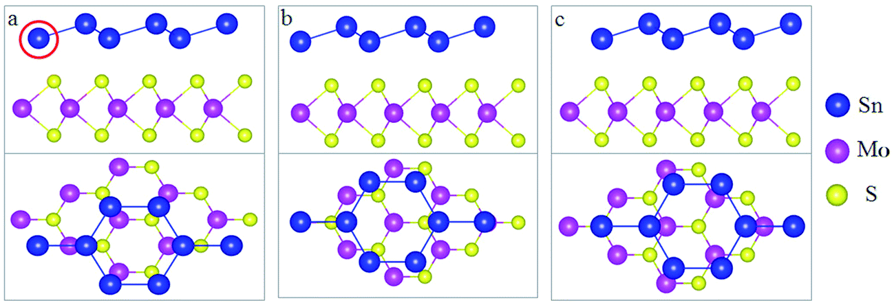 | ||
| Fig. 1 Side and top views of the three patterns of stanene/MoS2 HTS: (a) hollow pattern, (b) Mo pattern, and (c) S pattern. The blue, pink-purple, and yellow spheres represent Sn, Mo, and S atoms, respectively. | ||
The electronic properties of the isolated stanene and MoS2 monolayers have been discussed. Fig. 2(a) shows the energy band structure of stanene. There is a Dirac cone at the K point and an optical gap at the Γ point, consistent with the results obtained by Wang et al.29 and Zhu et al.30 It is clear that stanene is a gapless semiconductor and it has a large carrier mobility due to the Dirac cone, which is beneficial for potential applications in electric devices. However, for practical applications, a good substrate is necessary. Moreover, further orbital analyses suggest that the energy bands at the K point are composed of 5Pz hybrid orbitals of the Sn atoms, which ensures the stability of stanene by forming π-bonding. Fig. 2(b) shows the energy band structure of MoS2. MoS2 exhibits a semiconducting behavior with a direct band gap of 1.74 eV, which agrees well with previous studies,31 and the gap nearly covers the Dirac cone region of stanene. We expected that MoS2 may be an ideal substrate to tune the electric structure of stanene while contributing no additional transport channels near the Fermi surface. Based on these considerations, we investigated the electric properties of the stanene/MoS2 heterostructure in this study.
 | ||
| Fig. 2 Band structure of (a) 2D stanene and (b) MoS2 monolayer. | ||
To determine the stabilities for the three patterns of stanene/MoS2 HTSs, we calculated the binding energy, which is defined as follows:
| Eb = [E(stanene/MoS2) − E(stanene) − E(MoS2)]/N, |
| Configuration | Eb (meV) | Eg (meV) | d (Å) | meKM | meKΓ | mhKM | mhKΓ |
|---|---|---|---|---|---|---|---|
| Stanene/hollow | −39.63 | 76.5 | 3.26 | 0.0517m0 | 0.0566m0 | 0.0517m0 | 0.0568m0 |
| Stanene/Mo | −39.38 | 71.9 | 3.36 | 0.0481m0 | 0.0531m0 | 0.0479m0 | 0.0531m0 |
| Stanene/S | −39.75 | 73.2 | 3.34 | 0.0506m0 | 0.0554m0 | 0.0506m0 | 0.0555m0 |
To explore how the electronic structure of stanene can be affected by the MoS2 substrate, we examined the band structures of the stanene/MoS2 HTSs, as shown in Fig. 3. For the hollow pattern, due to the strong interaction between stanene and the MoS2 substrate, the high symmetry of the honeycomb-like structure of stanene is broken, and stanene undergoes a slight deformation that leads to opening a 76.5 meV band gap at the K point. However, the linear Dirac dispersion is nearly well-preserved, slightly away from the K point, suggesting that there is still a high carrier mobility for stanene grown on the MoS2 substrate. On the other hand, the binding energy of stanene/MoS2 (hollow) is −39.63 meV, as shown in Table 1. Therefore, it was easy to prepare stanene on a MoS2 substrate via the existing fabrication process such as high-speed centrifugation. It provides a possible way to prepare semiconductors with high carrier mobility for electronic applications. Compared with the hollow pattern, the Mo and S patterns presented similar results. Therefore, MoS2 is a good substrate for all three patterns considered herein.
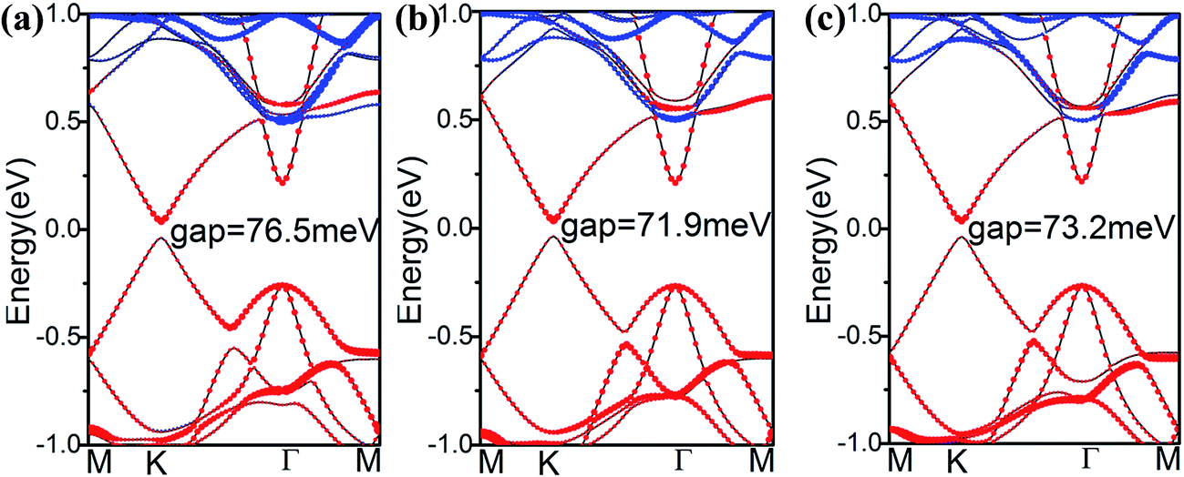 | ||
| Fig. 3 Band structures of stanene/MoS2 HTSs: (a) hollow pattern, (b) Mo pattern, and (c) S pattern. The red dots represent the contribution from Sn atoms, the blue dots represent the contribution from MoS2 and the black line represents the band structure of stanene/MoS2. | ||
The spin–orbit coupling (SOC) opened a band gap at the Dirac point, however, the associated gap due to rather weak second-order effective SOC was too small (∼10−3 meV), which makes the quantum spin Hall (QSH) effect in silicene and germanene only appear at an unrealistically low temperature.32,33 In addition, the GGA method usually underestimates the band gap. Therefore, we conducted calculations based on the hybrid HSE06 functional to assess the robustness of the results obtained herein with the PBE functional. Fig. 4(a) shows the DFT- and HSE-fitted band structures with SOC. It can be observed that the effect of SOC can change the value of the band gap but can not induce a band gap inversion in all systems. The band structure calculation at the PBE level reports a band gap of 11.9 meV, and HSE06 calculated results are essentially identical to the PBE results except for the increased band gap of 20.1 meV. We took the hollow pattern as an example to analyze the orbital components of the energy bands near the Fermi level. As shown in Fig. 4(b) and (d), we can find that the band gap at the K point is mainly due to the stanene layer, whereas orbitals due to MoS2 are mainly distributed in the energy region from 0.6 eV to 1.0 eV. As shown in Fig. 4(c), to further analyze the orbit components, we extracted and plotted the orbitals due to stanene by projecting the bands on different atomic orbitals. We found that the valence band maximum (VBM) and the conduction band minimum (CBM) near the Fermi level was two-fold degenerated with the features of binding states of Pz orbitals from the Sn atoms. At the Γ point, the VBM is formed by the Px and Pz orbitals of the Sn atoms, whereas the CBM contains the anti-bonding state features of Pz orbital. Overall, for the band structure, the main feature is the Pz orbital from the Sn atoms, which is similar to the band structure of isolated stanene. In isolated stanene, the Dirac point is protected by crystal symmetry. However, the match between stanene and the MoS2 substrate will break this symmetry, leading to the opening of a direct band gap. However, the MoS2 orbitals do not hybridize with the stanene orbitals at the K point near the Fermi level, and the only effect of the substrate is to tune the electronic structure at the K point, which suggests that MoS2 is an ideal substrate and electric carriers will transport through the stanene layer only.
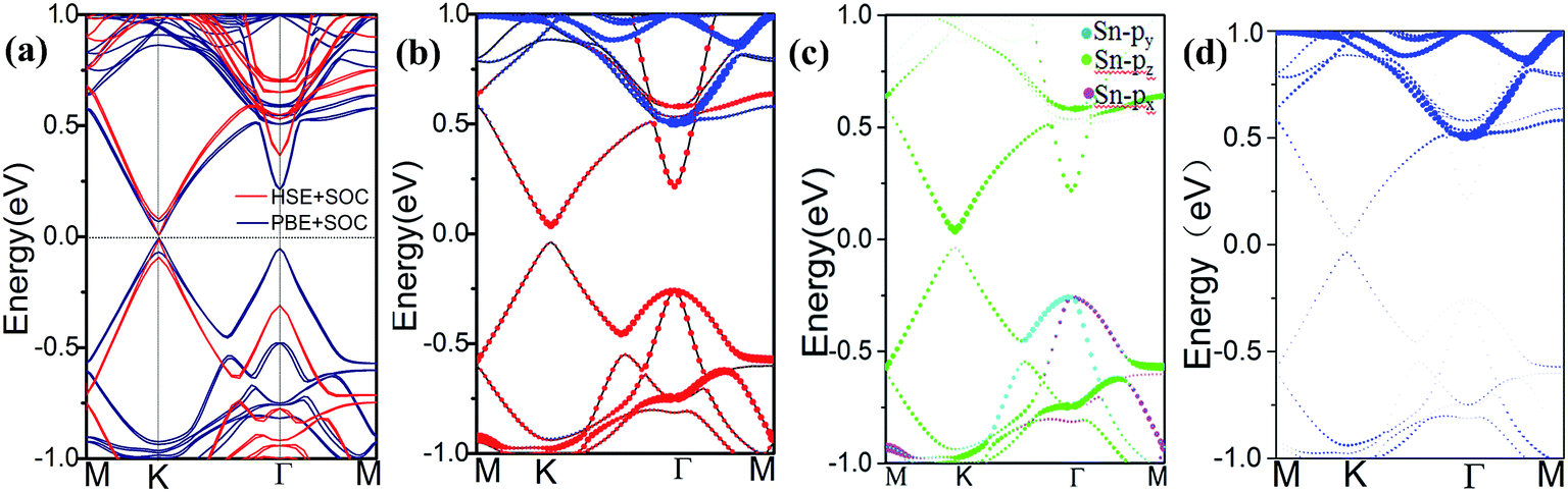 | ||
| Fig. 4 Band structure for the hollow pattern of the stanene/MoS2 HTS: (a) electronic band structure obtained based on PBE/HSE06 functional for the hollow-pattern stanene/MoS2 HTS including SOC; (b) orbital-resolved band structure for stanene/MoS2; (c) orbital-resolved band structure for stanene; and (d) orbital-resolved band structure for MoS2. The red dots represent the contribution from Sn atoms, the blue dots represent the contribution from MoS2, and the black line represents the band structure of stanene/MoS2. | ||
A high carrier mobility is essential for practical applications in field-effect-transistors.34 We estimated the carrier mobility of the stanene/MoS2 HTS by calculating the effective mass of electrons (me) and holes (mh) in the valence and conduction bands at the Dirac point of stanene/MoS2 for the three patterns of the HTSs, respectively. The effective particle mass is expressed as follows:35,36

By studying the structural stability, electric structure and carrier mobility, we found that MoS2 is an ideal substrate for stanene since it opens a band gap at the original Dirac point of isolated stanene and contributes no additional transport channels near the Fermi level. The band gap makes stanene/MoS2 HTS exhibit a large mobility and opening a band gap in this HTS will provide an ideal platform for potential applications in experiments and electronic devices. As it is known, external strain is a common method in the industry to tune the electric structure in semiconductors. In our material, we were tuned the interlayer spacing and the in-plane lattice constants of stanene and MoS2 by applying an external strain. In the following section, we showed how these two parameters tune the energy gap at the K point.
First, we investigated the effect of the interlayer distance on the electronic structure of stanene/MoS2. Our calculations indicate that there will always be an energy gap at the K point, which will maintain HTS as a semiconductor. In Fig. 5, we displayed the energy gap with respect to the spacing between the stanene and MoS2 layers for the hollow, Mo, and S patterns. One can observe that the gap size will decrease upon increasing the interlayer spacing. This is due to the effect of the MoS2 substrate on stanene layer that becomes weaker as the interlayer spacing increases, leading to the separation of two Sn–Pz bands from each other at the Fermi level. With respect to symmetry, as the interlayer spacing changes, the size of the induced band gap in stanene is related to symmetry breaking of the two stanene sublattices, which is due to the substrate (MoS2) effect and the stanene layer tends to recover the original symmetry,42–44 which preserves the Dirac point at the K point. In addition, with the decrease of interlayer spacing, the interactions between the stanene and MoS2 monolayers become stronger due to a symmetry breaking potential, thus leading to a decrease in the energy gap, as we can see in Fig. 5. Remarkably, for the distance of −0.2 Å, the largest gap about 77.4 meV, 73.0 meV, and 75.4 meV for hollow, Mo, and S patterns, respectively, was observed. The stanene/MoS2 still retains the semiconductor properties and the linear Dirac dispersion is nearly well-preserved, slightly away from the K point. The two layers would separate from each other when the interlayer spacing changes, which can cause a shift of the energy levels and thus a change in the band gap.
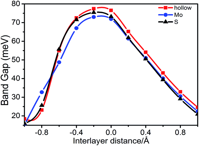 | ||
| Fig. 5 Band gap for the hollow, Mo, and S patterns, respectively, as a function of the spacing between the stanene and MoS2 monolayer. | ||
Elastic strain engineering is another route to continuously tune the energy gap. External strain will change the lattice constants measured by ε = (a − a0)/a0, where a (a0) is the lattice constant with (without) strain and ε denotes the strength of the strain. Fig. 6 presents the variation in the band gap of stanene/MoS2 for all three patterns under external strain ε. The strain has dramatic effects on the electronic properties of stanene/MoS2. If we observe the hollow pattern [Fig. 6(a)], we can see that increasing the lattice constant will continuously decrease the energy gap. A straightforward explanation is that the hopping strength or bonding energy is weakened, leading to a narrower energy range. Upon increasing the strain applied on stanene/MoS2, the lattice relaxes, the interactions between stanene and MoS2 are weakened, and the Sn–Sn bonds are stretched, thus weakening π-bonding between Sn atoms, leading to a smaller band gap. This result is similar to the results obtained in previous studies with a tight-binding model.45,46 Another effect of strain is to tune the Fermi level, with a metal–semiconductor phase transition occurring under a large enough strain. At a large enough tensile (compressive) strain, self-hole-doping (self-electron-doping) regime with hole (electron) carriers was observed.
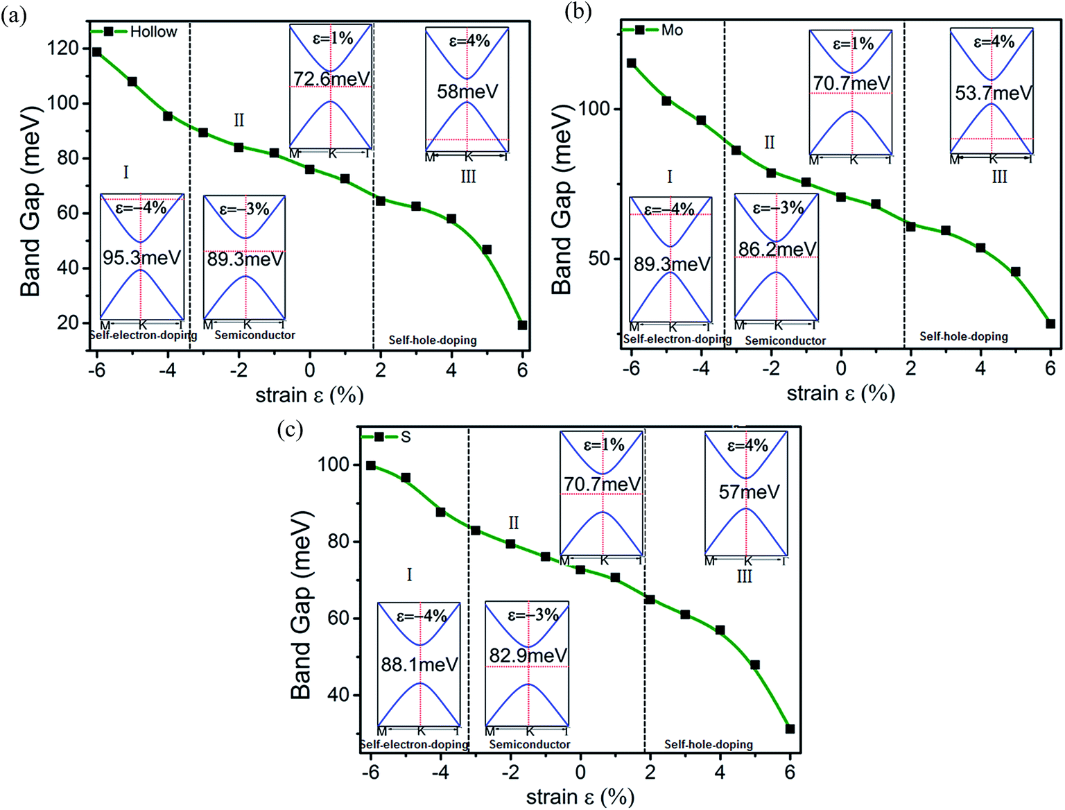 | ||
| Fig. 6 Changes in the band gap of the HTSs as a function of strain for the (a) hollow pattern, (b) Mo pattern, and (c) S pattern. | ||
Herein, it is demonstrated that strain can cause a metal–semiconductor phase transition, which is consistent with the common pressure-induced metal–insulator phase transitions in three-dimensional materials. The stanene/MoS2 heterostructure of Mo and S patterns under strain share properties qualitatively consistent with those of the hollow pattern and therefore a similar analysis applies as well, which has not been discussed herein. Our results show that the band gap in the stanene/MoS2 HTS can be conveniently tuned by external strain, making it a promising platform for applications in experiments and electronic devices.
IV. Conclusion
In summary, we systematically investigated the electronic properties of the stanene/MoS2 heterostructure by first-principles calculations. We calculated and determined the electronic structure for three different patterns of the free heterostructure, and then focused on the effect of an external strain, which would change the interlayer spacing and lattice constants in both the stanene and MoS2 layers. The MoS2 substrate induces an energy gap at the K point in stanene and preserves the linear Dirac dispersion slightly away from the K point while contributing no additional transport channels near the Fermi level. Our calculations suggest that the stanene/MoS2 heterostructure has a high carrier mobility, which is beneficial for electronic applications. Our results indicate that the band gap of all these HTSs can be continuously modulated by external strain to meet the demands in experiments and device design. In our opinion, the MoS2 substrate makes stanene a feasible platform to realize Sn-based nanostructures for applications in experiments and nanoelectronics.Acknowledgements
This work was supported by the National Natural Science Foundation of China (Grant No. 61571210, 61172028, 11274143, and 11304121).References
- A. K. Geim and K. S. Novoselov, Nat. Mater., 2007, 6, 183–191 CrossRef CAS PubMed.
- M. J. Allen, V. C. Tung and R. B. Kaner, Chem. Rev., 2010, 110, 132–145 CrossRef CAS PubMed.
- Q. Tang and Z. Zhou, Prog. Mater. Sci., 2013, 58, 1244–1315 CrossRef CAS.
- A. K. Geim, Science, 2009, 324, 1530–1534 CrossRef CAS PubMed.
- G. G. Guzman-Verri and L. C. Lew Yan Voon, Phys. Rev. B: Condens. Matter Mater. Phys., 2011, 76, 12825–12834 Search PubMed.
- K. S. Novoselov, A. K. Geim, S. V. Morozov, D. Jiang and Y. Zhang, Science, 2004, 306, 666–669 CrossRef CAS PubMed.
- K. S. Novoselov, A. K. Geim, S. V. Morozov, D. Jiang, M. I. Katsnelson, I. V. Grigorieva, S. V. Doubonos and A. A. Firsov, Nature, 2005, 438, 197–200 CrossRef CAS PubMed.
- D. L. Miller, K. D. Kubista, G. M. Rutter, M. Ruan, W. A. de Heer, P. N. First and J. A. Stroscio, Phys. Rev. B: Condens. Matter Mater. Phys., 2010, 81, 125427 CrossRef.
- Y. Jing, X. Zhang, D. H. Wu, X. D. Zhao and Z. Z. Hou, J. Phys. Chem. Lett., 2015, 6, 4252 CrossRef CAS PubMed.
- R. W. Zhang, C. W. Zhang, W. X. Ji, S. S. Li and S. J. Hu, New J. Phys., 2015, 17, 083036 CrossRef.
- F. F. Zhu, W. J. Chen, Y. Xu, C. L. Gao, D. D. Guan, C. H. Liu, D. Qian, S. C. Zhang and J. F. Jia, Nat. Mater., 2015, 14, 1020–1025 CrossRef CAS PubMed.
- B. Peng, H. Zhang, H. Z. Shao, Y. C. Xu, X. C. Zhang and H. Y. Zhu, Sci. Rep., 2016, 6, 20225 CrossRef CAS PubMed.
- M. Modarresi, A. Kakoee, Y. Mogulkoc and M. R. Roknabadi, Comput. Mater. Sci., 2015, 101, 164–167 CrossRef CAS.
- S. S. Li and C. W. Zhang, Mater. Chem. Phys., 2016, 173, 246–254 CrossRef CAS.
- R. W. Zhang, C. W. Zhang, W. X. Ji, S. S. Li, S. S. Yan, S. J. Hu, P. Li, P. Wang and F. Li, Sci. Rep., 2016, 6, 18879 CrossRef CAS PubMed.
- D. Wang, L. Chen, X. Wang, G. Cui and P. Zhang, Phys. Chem. Chem. Phys., 2015, 17, 26979–26987 RSC.
- Y. Fang, Z. Q. Huang, C. H. Hsu, X. Li, Y. Xu, Y. Zhou, F. Chuang and Z. Zhu, Sci. Rep., 2015, 5, 14196 CrossRef PubMed.
- G. Kresse and J. Furthmuller, Phys. Rev. B: Condens. Matter Mater. Phys., 1996, 54, 11169 CrossRef CAS.
- M. Houssa, B. van der Broek, E. Scalise, G. Pourtois, W. Afanas'ev and A. Stesmans, Phys. Chem. Chem. Phys., 2013, 15, 3702–3705 RSC.
- J. P. Perdew, K. Burke and M. Ernzerhof, Phys. Rev. Lett., 1996, 77, 3865 CrossRef CAS PubMed.
- J. P. Perdew, A. Ruzsinszky, G. I. Csonka, O. A. Vydrov, G. E. Scuseria, L. A. Constantin, X. Zhou and K. Burke, Phys. Rev. Lett., 2008, 100, 136406 CrossRef PubMed.
- G. Kresse and D. Joubert, Phys. Rev. B: Condens. Matter Mater. Phys., 1999, 59, 1758 CrossRef CAS.
- J. Heyd, G. E. Scuseria and M. J. Ernzerhof, J. Chem. Phys., 2003, 118, 8207 CrossRef CAS.
- J. Heyd, G. E. Scuseria and M. J. Ernzerhof, J. Chem. Phys., 2006, 124, 219906 CrossRef.
- H. J. Monkhorst and J. D. Pack, Phys. Rev. B: Condens. Matter Mater. Phys., 1976, 13, 5188 CrossRef.
- S. C. Wu, G. C. Shan and B. H. Yan, Phys. Rev. Lett., 2014, 113, 256401 CrossRef PubMed.
- C. Ataca, H. Şahin, E. Aktürk and S. Ciraci, J. Phys. Chem. C, 2011, 115, 3934–3941 CAS.
- K. F. Mak, K. L. He, C. G. Lee, G. H. Lee, J. Hone, T. F. Heinz and J. Shan, Nat. Mater., 2013, 12, 207–211 CrossRef CAS PubMed.
- H. Wang, S. T. Pi, J. Kim, Z. Wang and H. H. Fu, Phys. Rev. B: Condens. Matter Mater. Phys., 2016, 94, 035112 CrossRef.
- F. F. Zhu, W. J. Chen, Y. Xu, C. L. Gao and D. D. Guan, Nat. Mater., 2015, 14, 1020–1025 CrossRef CAS PubMed.
- K. F. Mak, C. Lee, J. Hone, J. Shan and T. F. Heinz, Phys. Rev. Lett., 2010, 105, 474–479 CrossRef PubMed.
- S. Cahangirov, M. Messer, E. Akturk, H. Sahin and S. Ciraci, Phys. Rev. Lett., 2009, 102, 236804 CrossRef CAS PubMed.
- C. C. Liu, W. X. Feng and Y. Q. Yao, Phys. Rev. Lett., 2011, 107, 076802 CrossRef PubMed.
- R. Zhang, C. Zhang, H. Luan, W. Ji and P. Wang, RSC Adv., 2015, 5, 35377–35383 RSC.
- R. W. Zhang, C. W. Zhang, W. X. Ji, S. J. Yan, S. S. Li, P. Li, P. J. Wang and Y. S. Liu, J. Phys. Chem. C, 2014, 118, 25278–25283 CAS.
- S. S. Li, C. W. Zhang, S. S. Yan, S. J. Hu, W. X. Ji, P. J. Wang and P. Li, J. Phys.: Condens. Matter, 2014, 26, 395003 CrossRef PubMed.
- R. Zhang, C. Zhang, W. Ji, F. Li, M. Ren, P. Li, M. Yuan and P. Wang, Phys. Chem. Chem. Phys., 2015, 17, 12194–12198 RSC.
- K. Chen, X. Wan and J. Xu, J. Mater. Chem. C, 2013, 1, 4869–4878 RSC.
- Y. P. Wang, W. X. Ji, C. W. Zhang, S. S. Li, F. Li, P. Li, M. J. Ren, X. L. Chen, M. Yuan and P. J. Wang, Mater. Chem. Phys., 2016, 173, 379–384 CrossRef CAS.
- S. S. Li, C. W. Zhang, W. X. Ji, F. Li, P. J. Wang and S. S. Yan, Phys. Chem. Chem. Phys., 2014, 16, 15968–15978 RSC.
- M. V. Fischetti and S. E. Laux, J. Appl. Phys., 1996, 80, 2234–2252 CrossRef CAS.
- L. Li and M. Zhao, J. Phys. Chem. C, 2014, 118, 19129–19138 CAS.
- L. Li, X. Wang, X. Zhao and M. Zhao, Phys. Lett. A, 2013, 377, 2628–2632 CrossRef CAS.
- L. Li and M. Zhao, Phys. Chem. Chem. Phys., 2013, 15, 16853–16863 RSC.
- M. Zhao, X. Zhang and L. Li, Sci. Rep., 2015, 5, 16108 CrossRef PubMed.
- M. Zhao, X. Chen, L. Li and X. Zhang, Sci. Rep., 2015, 5, 8441 CrossRef CAS PubMed.
| This journal is © The Royal Society of Chemistry 2017 |