
 Open Access Article
 This Open Access Article is licensed under a Creative Commons Attribution-Non Commercial 3.0 Unported Licence
Pressure-induced amorphization in the nanoindentation of single crystalline silicon
Jing Han *a,
Song Xub,
Jiapeng Sunc,
Liang Fangd and
Hua Zhua
*a,
Song Xub,
Jiapeng Sunc,
Liang Fangd and
Hua Zhua
aSchool of Mechanical and Electrical Engineering, China University of Mining and Technology, Xuzhou 221116, Jiangsu Province, PR China. E-mail: hanjing@cumt.edu.cn
bFaculty of Mechatronic and Materials Engineering, Xuhai College, China University of Mining and Technology, Xuzhou 221116, Jiangsu Province, PR China
cCollege of Mechanics and Materials, Hohai University, Nanjing 210098, Jiangsu Province, PR China
dState Key Laboratory for Mechanical Behavior of Materials, Xi'an Jiaotong University, Xi'an 710049, Shaanxi Province, PR China
First published on 5th January 2017
Abstract
Large-scale molecular dynamics simulations of nanoindentation on a (100) oriented silicon surface were performed to investigate the mechanical behavior and phase transformation of single crystalline silicon. The direct crystalline-to-amorphous transformation is observed during the nanoindentation with a spherical indenter as long as the applied indentation strain or load is large enough. This amorphization is accompanied by a distinct discontinuity in the load–indentation strain curves, known as “pop-in”. Herein, we have demonstrated the pressure-induced amorphization processes via direct lattice distortion. Moreover, the combination of large shear stress and associated hydrostatic pressure facilitates this crystalline-to-amorphous transformation. The structural characteristics, phase distribution, and phase transformation path have also been discussed in this study. The present results provide a new insight into the mechanical behavior and phase transformation of monocrystalline silicon.
1. Introduction
Silicon is widely known to exhibit pressure-induced polymorphism and amorphization, which has attracted significant attention for its important role in silicon's performance-related properties. The micro/nano-indentation has been extensively applied to investigate this matter both experimentally and theoretically in the past half-century. During nanoindentation, a high-pressure phase transformation (HPPT) from a semiconductor-like phase (pristine diamond cubic structure, Si-I) to a metallic phase is observed by in situ electrical measurements.1,2 This resulting metallic phase is identified as the β-Si phase with a body-centered-tetragonal structure based on the phase transformation sequences observed in the diamond-anvil cell experiments.2 While unloading, a sudden change in both the contact electrical resistance and load–displacement curves (known as pop-out) indicates the occurrence of a further phase transformation from the β-Si phase to the crystalline bc8/r8 phase, or an amorphous silicon (a-Si), or mixture of both (bc8/r8 and a-Si), depending on the unloading rate.3,4 The slow release rate endorses the crystal growth of the metastable bc8/r8 phase, whereas the fast unloading rate promotes amorphization. Molecular dynamics (MD) simulations confirm the formation of the β-Si phase and further show its structural characteristics and detailed distribution.5–10 In addition, another new high-pressure phase of bct5 with body-centered-tetragonal structure has been predicted.6,7,9 This result is supported by a recent in situ Raman microspectroscopy experiment.11 Further studies indicate that the phase transformation strongly depends on the maximum indentation load,4,12,13 load/unload speed,3,4,12–14 and the crystallographic orientation of the indented surface in nanoindentation.15,16All these research studies suggest that the crystalline-to-crystalline transformation (Si-I to β-Si and bct5) is the fundamental transformation mode during loading in nanoindentation. The crystalline-to-amorphous transformation must undergo a transition state of the crystalline β-Si and bct5 phases, i.e. the amorphous silicon is transformed from the intermediate high pressure crystalline β-Si and bct5 phases upon rapid unloading. However, direct crystalline-to-amorphous transformation is also reported, which challenges the necessity of high pressure phases during the crystalline-to-amorphous transformation. Gogotsi et al.17 provide an evidence that the amorphous silicon can be directly formed by the lattice distortion, induced by dislocation during the nanoindentation process using the Berkovich indenter. This defect accumulation-induced amorphization is further supported by some recent research studies. Shan et al.18 performed an advanced in situ TEM uniaxial compression of a nanoscale core/shell sample. The results unambiguously demonstrated that amorphous silicon is directly transformed from single crystalline silicon. No other intermediate crystalline phases were observed. Moreover, this direct amorphization can also be found in bulk silicon under dynamic shock compression.19 However, evidences for the direct amorphization are still rare in nanoindentation, especially with a spherical indenter.
In general, due to the large size and symmetrical nature of the spherical indenter, crystalline-to-crystalline transformation is promoted as the sole deformation mechanism in nanoindentation,20 whereas direct amorphization may be prevented. In this study, we report the direct crystalline-to-amorphous transformation in nanoindentation with a spherical indenter using MD simulations. We addressed this phenomenon by analyzing the detailed transformation process and stress mechanism.
2. Method
Large-scale MD simulations were performed based on the Tersoff potential to investigate the nanoindentation on a flat Si(100) surface.21 Fig. 1 shows the adopted MD simulation model. In this model, a spherical diamond indenter with a diameter of 20 nm, which was carved out of a (100) oriented diamond block, was used. The indenter is considered as a rigid body due to its superior hardness as compared to that of the silicon specimen. Two different single crystalline silicon specimens were used to test the effect of the finite system size: a small specimen with dimensions of 43.45 × 43.45 × 29.87 nm3 and a large specimen with dimensions of 65.17 × 65.17 × 40.73 nm3. The results indicate that the two specimens exhibit almost the same load–indentation strain curves, which implies that the small specimen is appropriate for this study. The total number of atoms that composed this silicon specimen was more than six million. To obtain the equilibrium configuration of the silicon specimens at a temperature of 300 K, a meticulous heat treatment process was performed, in which the temperature is controlled using the NVT ensemble with Langevin dynamics.22 The initial specimens, composed of silicon atoms with diamond cubic structure and with a lattice parameter of 5.431 Å, were first heated from 0 K to 600 K over 25 ps and this temperature was maintained over 25 ps. Then, the heated specimens were gradually cooled down to 300 K within 25 ps, subsequently followed by an annealing step at 300 K over 50 ps.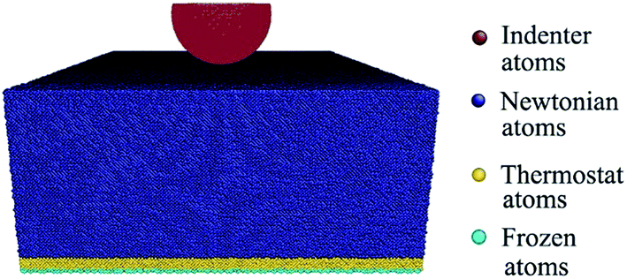 | ||
| Fig. 1 Molecular dynamics simulation model. | ||
After the initial construction, the MD simulations of nanoindentation were performed with a constant velocity of 80 m s−1 by the code of LAMMPS.23 The free boundary is applied along the indentation direction, whereas periodic boundary conditions were utilized along the other two directions. The bottom four atomic layers were frozen during the simulation to provide structural stability. The adjacent atomic layer with a 2 nm thickness maintained a constant temperature of 300 K to dissipate the excessive thermal energy. All the remaining atoms freely moved according to the Newtonian equations of motion.
A set of combined techniques consisting of modified coordination number (CN) considering the nearest and second nearest neighbors, radial distribution function (RDF) and bond angle distribution function (ADF) was applied to identify the six phases (Si-I, Si-II, Si-III, Si-XII, bct5, and a-Si) observed in the previous studies.9 In our MD simulations, we have not found a large Si-III/Si-XII phase region either under loading or unloading. Instead, we found many isolated Si-III/Si-XII atoms around the transformation region. Further analyses indicated that these atoms have a slightly distorted diamond cubic structure (DDS) rather than the structure of the Si-III/Si-XII phase. Therefore, in this study, we employed DDS instead of Si-III/Si-XII atoms. A detailed description of these combined techniques and analyses of the DDS can be found in our prior report.9
3. Results
3.1 Load–indentation strain curve
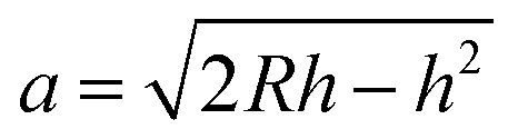
To compare the results of nanoindentation with different radii of indenter, the characteristic indentation strain ε is employed to take the place of the generally used indentation depth. The indentation strain ε is defined as follows:| ε = 0.2(h/a) | (1) |
 | (2) |
Fig. 2 shows the load–indentation strain (L–ε) curve for the Si(100) surface induced by nanoindentation. A distinct discontinuity of the L–ε curve can be found at ε = 0.146, which is the so called “pop-in” event. Beyond this point, the shape change of the L–ε curve implies a transformation of the deformation mechanism. This pop-in is generally found in the experiments and widely accepted as a signal of the HPPT from the Si-I to the β-Si phase. Herein, note that the present pop-in event differs from those observed in the experiments. The analyzation of the HPPT indicates that the plastic deformation begins at ε = 0.069, but no noticeable pop-in event is observed, as shown in Fig. 1. The possible reasons lie in the extremely small radius of the indenter and tremendous indentation speed used in the MD simulation, contrary to an experiment. With this result, multiple occurrences of the pop-in events should be detected in nanoindentation on a Si(100) surface with low velocity and a large indenter, which has been reported in an experiment.24
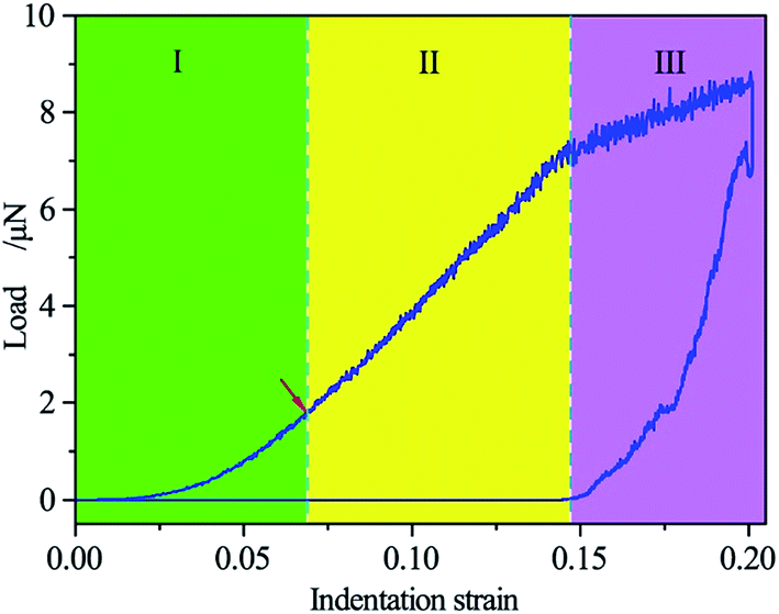 | ||
| Fig. 2 L–ε curve for the Si(100) surface. The red arrow marks the onset of the plastic deformation or phase transformation. | ||
Considering the pop-in and the onset of the plastic deformation, the L–ε curve can be divided into three stages, as indicated in Fig. 1. In stage I, the single crystalline silicon undergoes a reversible elastic deformation. From the beginning of stage II, the plastic deformation occurs, processed by HPPT. Thus, the high-pressure phases can be observed in both stage II and III; however, the type and distribution of the high-pressure phases are very different in these two stages, as described in detail below.
3.2 HPPT in nanoindentation
Fig. 3 illustrates the evolution of the high-pressure phases during loading in nanoindentation on the Si(100) surface, in which the high-pressure phases are identified and colored according to the modified coordination number. At a small ε (less than 0.146), the crystalline β-Si phase and bct5 phase are the only two high-pressure phases, as shown in Fig. 3(a). Several β-Si single-phase regions can be found below the indenter. Among these, a large isolated β-Si single-phase region lies in the center of the transformation region, and another four small β-Si single-phase regions are distributed around this large region along the ±[100] and ±[010] directions. The bct5 phase is distributed around the β-Si phase regions and fills the rest of the transformation region. However, the atomic layer with several nanometers directly beneath the indenter has not undergone any phase transformation. Around the phase transformation region, a large number of isolated atoms with distorted diamond structure can be found, which indicates that these atoms underwent a large deformation. The detailed structural characteristics and distribution of the high-pressure phase are consistent with those reported in our previous studies9,25 and other study.6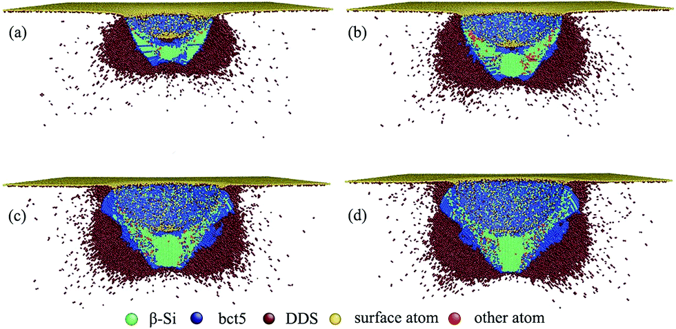 | ||
| Fig. 3 Side cross-section views on the (010) plane of the high-pressure phase distribution during loading at ε = (a) 0.119, (b) 0.149, (c) 0.18, and (d) 0.2. | ||
When the ε increases over the critical value of 0.146, a great shift of the high-pressure phases takes place. The β-Si phase and bct5 phase are no longer the only two high-pressure phases since the a-Si phase begins to appear in the transformation region. With the increase in ε, the large isolated β-Si phase region in the center of the transformation region continuously expands, whereas the four small β-Si regions are gradually substituted by the a-Si phase, as shown in Fig. 3(b)–(d). This implies the occurrence of direct amorphization. The observed untransformed region directly beneath the indenter at small ε is gradually occupied by the β-Si phase at large ε. As a result, a new map of high-pressure phases at large ε appears, which is dramatically different from the previously reported results, as indicated in Fig. 3(d).
Fig. 4 is a series of the cross-section views, which shows the distribution of the high-pressure phases at ε = 0.2. The phase transformation region can be divided into upside and underside by the bottom of the indenter [marked by the dashed line in Fig. 4(a)]. In the underside region, β-Si phase, bct5 phase, and a-Si phase coexist, as indicated in Fig. 4(a)–(c). The single β-Si phase region is located beneath the indenter. The bct5 phase distributes around the β-Si phase and forms a four-fold symmetrical pattern [as shown in Fig. 4(b) and (c)]. The a-Si fulfills the gap between the β-Si and bct5 phase regions. In the upside region, a large number of the a-Si atoms are distributed alongside the indenter, and the bct5 phase is located around the a-Si phase, as shown in Fig. 4(d) and (e). Although the bct5 phase region shows similar four-fold symmetrical patterns in the upside and underside regions, the direction of the patterns is entirely different. The bct5 phase region is distributed along the ±[100] and ±[010] directions in the upside region [see Fig. 4(d) and (e)], whereas along the ±[110] and ±[1![[1 with combining macron]](https://www.rsc.org/images/entities/char_0031_0304.gif) 0] directions in the underside region [see Fig. 4(b) and (c)].
0] directions in the underside region [see Fig. 4(b) and (c)].
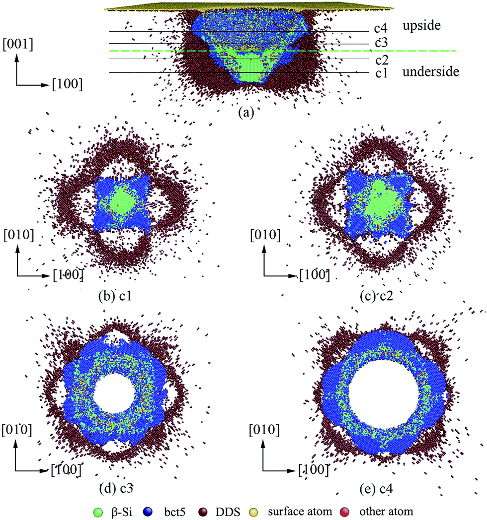 | ||
| Fig. 4 The high-pressure phases distribution at ε = 0.2. (a) Side cross-section view on the (010) plane sketching the location of the following cross-section. Cross-section views of the high-pressure phases on the (001) plane at location of (b) c1, (c) c2, (d) c3, (e) c4 of (a). | ||
3.3 The process of the HPPT
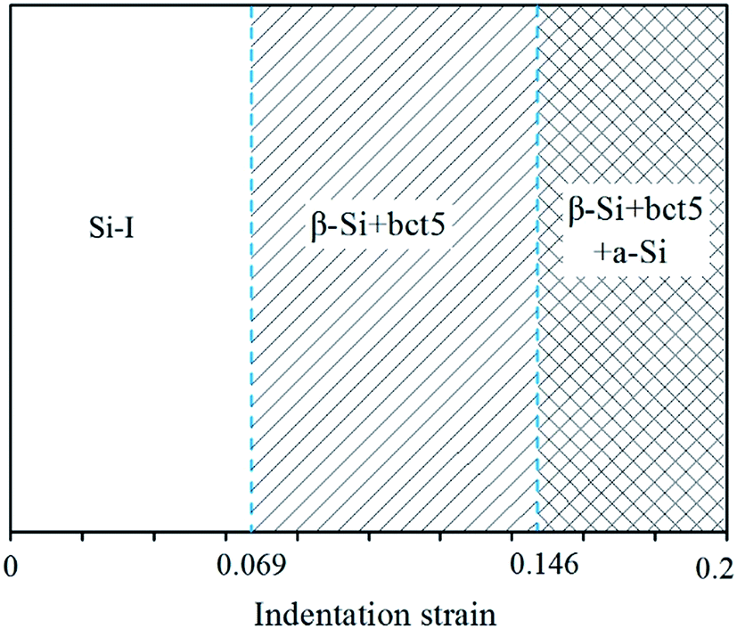
The detailed process of the HPPT at a small indentation strain has been discussed in previous reports,6,7,9,25 in which the pristine silicon continually transforms into β-Si and bct5 phases. In this section, we focus on the formation of the a-Si phase.The evolution of the high-pressure phases (see Fig. 3) indicates that the phase transformation process with the increasing ε can be divided into two stages with a critical ε of 0.146. In the first stage, the pristine diamond structure silicon continuously transforms into crystalline β-Si phase and bct5 phase, which results in the rapid expansion of the β-Si and bct5 phase regions. In the second stage, the β-Si phase and bct5 phase continuously expand. Moreover, the pristine silicon and a part of the β-Si phase and bct5 phase gradually transform into the a-Si phase. The formed a-Si phase distributes around the indenter, which directly provides support force to the indenter. Hence, the plastic flow of a-Si dominates the deformation process in this stage. The difference in the deformation mode leads to the discontinuity point in the L–ε curve. Hence, the formation of the a-Si phase is responsible for the pop-in event in the L–ε curve. In summary of these observations, a map can be compiled, as shown in Fig. 5, to show the high-pressure phases as a function of ε under the present conditions.
 | ||
| Fig. 5 Map of the high-pressure phases during nanoindentation on a Si(100) surface. | ||
3.4 Structural characteristics of a-Si phase
Fig. 6 shows the radial distribution function (RDF) and bond angle distribution function (ADF) of the a-Si phase during loading in a selected cuboid region. The disappeared third RDF peak, broadened RDF, and ADF peaks confirm the amorphous characteristic. The first RDF peak appears at a distance of 0.248 nm, which is slightly larger than that of the perfect cubic diamond structured silicon (0.235 nm). The centered peak of ADF is shifted to 76.50°, and there is a small peak near 58.50°. This is very different from that of the perfect cubic diamond structured silicon, whose ADF has a single peak at 109°. Careful calculation shows that the average coordination number of the a-Si phase is 6.70, which is consistent with the experimental value of 6.40 (ref. 26) and the CP simulation result of 6.5 (ref. 27 and 28) for liquid silicon. The proportion of 5- and 6-coordinate silicon atoms approaches ∼82.80%. Moreover, the volume per atom of a-Si is 0.750 relative to the zero-temperature diamond structure. These structure parameters are in accordance with the high density a-Si phase (HDA). Hence, the a-Si phase observed during the loading of nanoindentation on Si(100) is the HDA phase with a dense network structure, as shown in the inset of Fig. 6.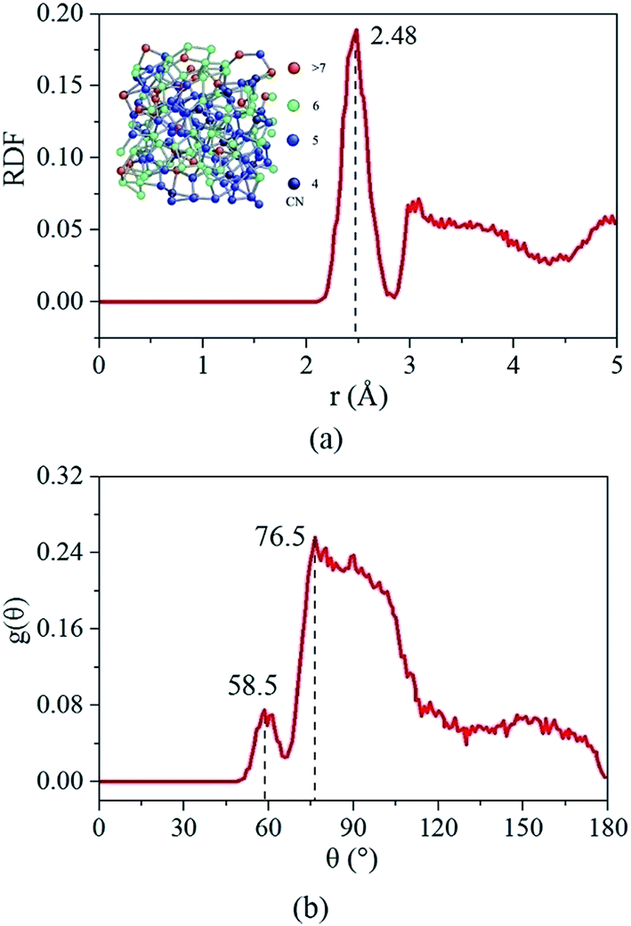 | ||
| Fig. 6 (a) RDF and (b) ADF of a-Si. The inset shows the network structure of a-Si, in which atoms are colored according to the coordination number (CN). | ||
4. Discussion
The present results indicate that the direct crystalline-to-amorphous transformation can occur in nanoindentation on Si(100) with a spherical indenter as long as the applied indentation strain or load is large enough. The amorphization initiates at the large indentation strain of 0.146 under the present simulation conditions. Why does the amorphization appear at a large indentation strain? Our MD simulations indicate that the large shear stress and associated hydrostatic pressure drive this amorphization. With the increase in the indentation strain, the shear stress becomes larger and larger, as shown in Fig. 7. At a large indentation strain, the β-Si and bct5 phases at the edge of the transformation region undergo very large shear stress and associated hydrostatic pressure. However, the β-Si phase directly beneath the indenter sustains very low shear stress and high hydrostatic stress, as indicated in Fig. 6(b). When the shear stress is large enough, the generated bct5 phase, β-Si phase, and pristine silicon can all transform into the a-Si phase. Conversely, the low shear stress and high hydrostatic stress in the region directly beneath the indenter promote the continual expansion of the β-Si phase region in the further indentation process.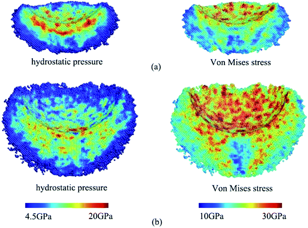 | ||
| Fig. 7 Distribution of the hydrostatic pressure and Von Mises stress at ε = (a) 0.119 and (b) 0.20. Stress is averaged over a 0.5 nm spherical volume around each atom, and the atoms whose hydrostatic pressure is below 4.5 GPa are invisible. | ||
The present result emphasizes that it is the large shear stress and associated hydrostatic pressure that facilitate the direct crystalline-to-amorphous transformation rather than single large shear stress, which is just like the case of nanoindentation at a large indentation strain. The crystalline-to-amorphous transformation of silicon has been observed under other loading conditions, which provides more evidence for this viewpoint. In nanoscratching, where the shear stress is much larger than the hydrostatic pressure, amorphization processes act as the dominant transformation mode.9 Direct crystalline-to-amorphous transformation is also observed in the shock compression of single crystalline silicon19,29 and in the uniaxial compression of the core/shell configurations,18 in which the hydrostatic pressure is considered as another essential condition besides the large shear stress. Conversely, the combination of high hydrostatic pressure and low or even no shear stress triggers the crystalline-to-crystalline transformation, which is the situation of the nanoindentation carried out at a low indentation strain and the high-pressure experiment. In the diamond-anvil cell experiments, the crystalline-to-crystalline transformation and the absence of a-silicon provide a reliable evidence for this conclusion. Although the existing research studies and the present simulation indicate that different combinations of hydrostatic pressure and shear stress induce a variety of phase transformations, a quantitative description is still an open question, which is outside the scope of this article.
In the shock compression of single crystalline silicon19,29 and uniaxial compression of the core/shell configuration,18 the crystalline-to-amorphous transformation is conducted through defect accumulation. Herein, we did not find any defects, such as dislocation and stacking faults, in the simulation. As previously mentioned, the silicon atoms surrounding the transformation region undergo severe lattice distortion, as shown in Fig. 3 and 4. We consider that it is just the lattice distortion that induces the crystalline-to-amorphous transformation in the present simulation of nanoindentation. In fact, the lattice distortion-induced amorphization has been observed in the unloading of nanoindentation.17 The defect accumulation-induced amorphization may become true in the nanoindentation process at large enough indentation strain, where the defects could initialize and develop besides the phase transformation. Unfortunately, this is beyond the ability of the Tersoff potential.
While unloading, the pressure-induced a-Si could further transform through two possible paths. In the first possible transformation path, the a-Si phase is retained when the unloading process is fast enough, similar to quenching. This is the only path that can be predicted by the MD simulation, as only the fast unloading process can be simulated since it is limited by the computational capability and intrinsic algorithm. In the second possible transformation path, the a-Si phase crystallizes into pristine diamond structured silicon or into Si-III and Si-XII phases. This is evidenced by the observed crystalline pockets embedded in the a-Si region.17,30,31
Under the present conditions, the critical strain for the crystalline-to-amorphous transformation reaches 0.146. Considering the overestimated melting temperature by the Tersoff potential, the real critical strain should be smaller than 0.146. In nanoindentation with a spherical indenter, it is difficult to achieve this critical strain for the limited load of the present instrument. Therefore, it is very difficult to observe the amorphization under the present experimental conditions. However, the critical strain can be easily achieved by a sharp indenter, such as Vickers, Berkovich, and cube corner indenters. Moreover, the direct amorphization with a Berkovich indenter has been reported,14 which indirectly verifies the present results.
5. Conclusion
We perform the large-scale molecular dynamics simulations of nanoindentation on the (100) surface of the single crystalline silicon with a spherical indenter. A clear evidence that the HPPT depends on the indentation strain is presented. At low indentation strain (in the range from 0.069 to 0.146), the pristine single crystalline silicon transforms into crystalline β-Si and bct5 phases. Once the indentation strain exceeds the critical value of 0.146, the direct crystalline-to-amorphous transformation can be observed without any intermediate crystalline phase. Accompanying this amorphization, a distinct pop-in event is observed in the load–indentation strain curve. Further investigations indicate that the pressure-induced amorphization proceeds through lattice distortion. The combination of large shear stress and associated hydrostatic pressure facilitate this direct crystalline-to-amorphous transformation. Considering this, multiple occurrences of pop-in events and multiple possible phase transformation paths are suggested in the nanoindentation process under the experimental conditions.Acknowledgements
The authors acknowledge the financial support received from the Fundamental Research Funds for the Central Universities (Grant No. 2014QNA36), National Natural Science Foundation of China (Grant No. 51505479) and Jiangsu Natural Science Foundation of China (Grant No. BK20150184). We are also grateful to the Advanced Analysis and Computation Center of CUMT for the award of CPU hours to accomplish this study.References
- D. R. Clarke, M. C. Kroll, P. D. Kirchner, R. F. Cook and B. J. Hockey, Phys. Rev. Lett., 1988, 60, 2156 CrossRef CAS PubMed.
- J. E. Bradby, J. S. Williams and M. V. Swain, Phys. Rev. B: Condens. Matter Mater. Phys., 2003, 67, 0852058 CrossRef.
- S. Ruffell, J. E. Bradby, J. S. Williams and P. Munroe, J. Appl. Phys., 2007, 102, 063521 CrossRef.
- J. I. Jang, M. J. Lance, S. Q. Wen, T. Y. Tsui and G. M. Pharr, Acta Mater., 2005, 53, 1759–1770 CrossRef CAS.
- W. Cheong and L. C. Zhang, Nanotechnology, 2000, 11, 173–180 CrossRef CAS.
- D. E. Kim and S. I. Oh, Nanotechnology, 2006, 17, 2259–2265 CrossRef CAS.
- D. E. Kim and S. I. Oh, J. Appl. Phys., 2008, 104, 0135021 Search PubMed.
- P. Eyben, F. Clemente, K. Vanstreels, G. Pourtois, T. Clarysse, E. Duriau, T. Hantschel, K. Sankaran, J. Mody, W. Vandervorst, K. Mylvaganam and L. C. Zhang, J. Vac. Sci. Technol., B: Nanotechnol. Microelectron.: Mater., Process., Meas., Phenom., 2010, 28, 401–406 CAS.
- J. Sun, L. Fang, J. Han, Y. Han, H. Chen and K. Sun, Comput. Mater. Sci., 2014, 82, 140–150 CrossRef CAS.
- C. F. Sanz-Navarro, S. D. Kenny and R. Smith, Nanotechnology, 2004, 15, 692–697 CrossRef CAS.
- Y. B. Gerbig, C. A. Michaels, A. M. Forster and R. F. Cook, Phys. Rev. B: Condens. Matter Mater. Phys., 2012, 85, 390–406 CrossRef.
- T. Juliano, V. Domnich and Y. Gogotsi, J. Mater. Res., 2004, 19, 3099–3108 CrossRef CAS.
- L. Chang and L. C. Zhang, Acta Mater., 2009, 57, 2148–2153 CrossRef CAS.
- C. R. Das, S. Dhara, Y. R. Jeng, P. C. Tsai, H. C. Hsu, B. Raj, A. K. Bhaduri, S. K. Albert, A. K. Tyagi, L. C. Chen and K. H. Chen, Appl. Phys. Lett., 2010, 96, 253113 CrossRef.
- Y. B. Gerbig, S. J. Stranick, D. J. Morris, M. D. Vaudin and R. F. Cook, J. Mater. Res., 2009, 24, 1172–1183 CrossRef CAS.
- Y. B. Gerbig, S. J. Stranick and R. F. Cook, Phys. Rev. B: Condens. Matter Mater. Phys., 2011, 83, 205209 CrossRef.
- D. B. Ge, V. Domnich and Y. Gogotsi, J. Appl. Phys., 2003, 93, 2418–2423 CrossRef CAS.
- Y. Wang, W. Zhang, L. Wang, Z. Zhuang, E. Ma, J. Li and Z. Shan, NPG Asia Mater., 2016, 8, e291 CrossRef CAS.
- S. Zhao, E. N. Hahn, B. Kad, B. A. Remington, C. E. Wehrenberg, E. M. Bringa and M. A. Meyers, Acta Mater., 2016, 103, 519–533 CrossRef CAS.
- S. Wong, B. Haberl, J. S. Williams and J. E. Bradby, Appl. Phys. Lett., 2015, 106, 205901 Search PubMed.
- J. Tersoff, Phys. Rev. B: Condens. Matter Mater. Phys., 1989, 39, 5566–5568 CrossRef.
- T. Schneider and E. Stoll, Phys. Rev. B: Condens. Matter Mater. Phys., 1978, 17, 1302–1322 CrossRef CAS.
- S. Plimpton, J. Comput. Phys., 1995, 117, 1–19 CrossRef CAS.
- T. Juliano, V. Domnich and Y. Gogotsi, J. Mater. Res., 2004, 19, 3099–3108 CrossRef CAS.
- J. Sun, A. Ma, J. Jiang, J. Han and Y. Han, J. Appl. Phys., 2016, 119, 95904 CrossRef.
- Y. Waseda and K. Suzuki, Z. Phys. B. Condens. Matter, 1975, 20, 339–343 CAS.
- I. Stich, R. Car and M. Parrinello, Phys. Rev. Lett., 1989, 63, 2240–2243 CrossRef CAS PubMed.
- R. Car, M. Parrinello and I. Štich, Phys. Rev. B: Condens. Matter Mater. Phys., 1991, 44, 4262–4274 CrossRef.
- S. Zhao, B. Kad, E. N. Hahn, B. A. Remington, C. E. Wehrenberg, C. M. Huntington, H. S. Park, E. M. Bringa, K. L. More and M. A. Meyers, Extreme Mech Lett., 2015, 5, 74–80 CrossRef.
- Y. Q. Wu, H. Huang, J. Zou, L. C. Zhang and J. M. Dell, Scr. Mater., 2010, 63, 847–850 CrossRef CAS.
- Z. Y. Zhang, Y. Q. Wu, D. M. Guo and H. Huang, Scr. Mater., 2011, 64, 177–180 CrossRef CAS.
| This journal is © The Royal Society of Chemistry 2017 |