
 Open Access Article
 This Open Access Article is licensed under a
 Creative Commons Attribution 3.0 Unported Licence
A novel TiO2 nanostructure as photoanode for highly efficient CdSe quantum dot-sensitized solar cells†
Y. B. Lua,
L. Li *a,
S. C. Sub,
Y. J. Chenc,
Y. L. Songa and
S. J. Jiaod
*a,
S. C. Sub,
Y. J. Chenc,
Y. L. Songa and
S. J. Jiaod
aKey Laboratory for Photonic and Electronic Bandgap Materials, Ministry of Education, School of Physics and Electronic Engineering, Harbin Normal University, Harbin 150025, PR China. E-mail: physics_lin@hotmail.com
bInstitute of Opto-electronic Materials and Technology, South China Normal University, Guangzhou, 510631, PR China
cKey Laboratory of In-Fiber Integrated Optics, Ministry of Education and College of Science, Harbin Engineering University, Harbin 150001, PR China
dSchool of Materials Science and Engineering, Harbin Institute of Technology, Harbin 150001, P. R. China
First published on 1st February 2017
Abstract
For sensitized solar cells, photoanodes combining the advantages of TiO2 nanoparticles (high specific surface area) and one-dimensional (1D) nanostructures (fast transport channels) are ideal for obtaining highly efficient sensitized solar cells. In this paper, 1D connected TiO2 nanoparticles (1D CTNPs) were synthesized by a simple one-pot solvothermal reaction and utilized to fabricate CdSe quantum dot-sensitized solar cells (QDSSCs). To evaluate the effects of the 1D CTNPs on the performance of CdSe QDSSCs, another CdSe QDSSC was fabricated based on conventional TiO2 nanoparticles (TNPs), which were synthesized via a similar solvothermal route with a different reaction time. The 1D CTNP-based CdSe QDSSC showed an impressive light-to-electricity conversion efficiency of 5.45% accompanying an open-circuit voltage of 596 mV, a fill factor of 0.52, and a short-circuit current density of 17.48 mA cm−2. This efficiency is much higher than that of the TNP-based cell (4.00%). The significant enhancements in the open-circuit voltage, short-circuit current, and power conversion efficiency of the 1D CTNP-based CdSe QDSSC compared to the TNP-based cell are explained as follows. The 1D CTNP photoanode has large pores and a relatively high specific surface area, facilitating the loading of CdSe QDs and, most importantly, providing an efficient electron transport pathway, which effectively facilitates electron transport and prolongs electron lifetime. The excellent properties of the 1D CTNPs make them an optimal candidate as a photoanode material for highly efficient QDSSCs.
1. Introduction
The rapid development of the global economy, people's increasing demand for energy, global environmental problems, and depletion of fossil fuels have forced the exploration of clean, regenerative energy. The development of photovoltaic devices have opened up a new opportunity to use solar energy.1,2 As one type of cost-effective, third-generation photovoltaic cells, CdSe quantum dot-sensitized solar cells (QDSSCs) have drawn much attention because of their intrinsic advantages compared to other photovoltaic devices, such as superior extinction coefficient, solution processing ability, and tunable band gap based on QD size.3–8 Furthermore, with the possibility of multiple exciton generation, the theoretical photovoltaic conversion efficiency in QDSSCs is 44%, which is much higher than that of semiconductor solar cells (31%) according to the Schockley–Queisser limit.9,10The photovoltaic conversion efficiencies of QDSSCs have increased rapidly from ∼1% to ∼12% as a result of research efforts in recent years.7,11–14 However, there is still a large gap between the conversion efficiencies of practical QDSSC devices and the theoretical limit (44%), indicating that the photoanode, QDs, interface recombination, electrolyte and counter electrode in QDSSCs have still not been optimized. As a significant part of a QDSSC, the metal-oxide photoanode acts as a scaffold to anchor the QD sensitizers and provides a pathway to transport the photo-generated electrons. Generally, TiO2 nanoparticles (TNPs) with sizes of 10–30 nm, which offer sufficient specific areas for QDs loading, are the most widely used material to fabricate photoanodes. However, the TNPs-based photoanode provide a random a pathway for electron transport, where exists large numbers of defects and grain boundaries,15–17 which seriously restricts the transport of electrons and enhances electron recombination, thus further increasing the electron transport time and decreasing the electron lifetime. Finally, the TNP-based photoanode would suffer from poor charge transport and collection efficiency. The TiO2 nanoparticles also show inefficient light scattering ability, resulting in poor light-harvesting efficiency. One-dimensional (1D) nanostructures such as nanowires and nanotubes are considered as promising candidates to overcome the shortcomings of TNPs because they can provide direct pathways for electron transport, thus facilitating electron transport and suppressing charge recombination.18,19 However, 1D nanostructures usually have low specific surface areas, leading to low QD loading and low QDSSC conversion efficiency compared to TNP-based cells.20 Specially, some photoanodes with 1D nanostructures have been grown directly on conductive substrates, which is not convenient for the fabrication of large surfaces; however, fabricating photoanodes via screen-printing methods could overcome this problem.
In this paper, a unique TiO2 nanostructure was synthesized by a simple one-pot solvothermal reaction, which is formed by self-assembly of TiO2 nanoparticles into one-dimensional nanostructure. These nanostructures are termed 1D connected TiO2 nanoparticles (1D CTNPs). To test the performance of the photoanode based on 1D CTNPs in QDSSCs, the 1D CTNP-based photoanode fabricated via screen printing was used to assemble CdSe QDSSCs. The performance of the new CdSe QDSSCs was compared to that of CdSe QDSSCs based on a conventional TNP photoanode synthesized in the same way but with a different reaction time. The 1D CTNP-based CdSe QDSSC shows an impressive light-to-electricity conversion efficiency of 5.45% accompanying an open-circuit voltage (Voc) of 596 mV, a fill factor (FF) of 0.52, and a short-circuit current density (Jsc) of 17.48 mA cm−2. This conversion efficiency is much higher than that of the TNP-based cell (4.00%). The significant enhancements in the open-circuit voltage, short-circuit current, and power conversion efficiency (PCE) of the 1D CTNP-based CdSe QDSSC compared to the TNP-based cell are explained as follows. The 1D CTNP photoanode has large pores and a relatively high specific surface area, facilitating the loading and filling with CdSe QDs and, most importantly, providing an efficient electron transport pathway, which effectively facilitates electron transport and prolongs electron lifetime.
2. Experimental section
Materials
Cadmium oxide (99.99%), selenium power (99.99%), oleylamine (OAM), 1-octadecene (ODE, 90%), trioctylphosphine (TOP, 90%), terpineol and ethyl cellulose (EC) were purchased from Aldrich. Oleic acid (OA, 90%) and 3-mercaptopropionic acid (MPA, 99%) were obtained from Alfa. Acetic acid (HAc) and tetrabutyltitanate (TBT) were purchased from Sinopharm Chemical Reagent Company Limited. All chemicals were used as received without further purification.Synthesis of oil-soluble CdSe QDs
Briefly, a Cd stock solution (0.4 M) was prepared by dissolving CdO in oleic acid and ODE (v/v, 1![[thin space (1/6-em)]](https://www.rsc.org/images/entities/char_2009.gif) :1) at 250 °C under N2 atmosphere. A Se stock solution (1 M) was obtained by dissolving Se power in TOP under ultrasonic sonication. Se stock solution (0.2 mL), 4.5 mL OAM and 0.3 mL TOP were mixed in a 50 mL three-necked flask, and the mixture was heated to 300 °C under N2 atmosphere with stirring. Subsequently, 0.5 mL of Cd stock solution was injected into the reaction flask, and the temperature was set to 280 °C for the growth and annealing of nanocrystals. The obtained CdSe QDs were precipitated by adding methanol and acetone into the hexane solution and further isolated and purified by centrifugation.
:1) at 250 °C under N2 atmosphere. A Se stock solution (1 M) was obtained by dissolving Se power in TOP under ultrasonic sonication. Se stock solution (0.2 mL), 4.5 mL OAM and 0.3 mL TOP were mixed in a 50 mL three-necked flask, and the mixture was heated to 300 °C under N2 atmosphere with stirring. Subsequently, 0.5 mL of Cd stock solution was injected into the reaction flask, and the temperature was set to 280 °C for the growth and annealing of nanocrystals. The obtained CdSe QDs were precipitated by adding methanol and acetone into the hexane solution and further isolated and purified by centrifugation.
Preparation of water-soluble MPA-capped CdSe QDs
Typically, 1.0 mL of MPA–methanol solution (160 μL MPA added to 1 mL methanol and adjusted to pH 11 with 30% NaOH aqueous solution) was added into 20 mL of a solution of CdSe QDs in chloroform and stirred for 2 h to precipitate the QDs. Then, 20 mL water was injected into the mixture and stirred for another 10 min. The aqueous phase containing QDs was collected and purified with acetone. Finally, the water-soluble MPA-capped CdSe QDs aqueous solution was obtained by adding 1 mL water.Synthesis of two TiO2 nanostructures
To compare the effects of the TNP-based and 1D CTNP-based photoanodes on the performances of the QDSSCs, the two TiO2 nanostructures were synthesized under the same conditions but with different reaction times. In detail, 1 mL of TBT was added dropwise to 30 mL HAc with rigorous magnetic stirring and kept for 30 min at room temperature. The obtained white solution was transferred into a 50 mL Teflon-lined stainless-steel autoclave, which was placed in an electronic oven and maintained at 160 °C for 10 min (TNPs) or 30 min (1D CTNPs). After the autoclaves were cooled to room temperature naturally, the two nanostructured products were obtained by freeze-drying and then annealed at 500 °C for 3 h to remove the residual organics.Preparation of screen-printing pastes
To prepare the mesoporous TiO2 pastes, 0.5 g TNPs or 1D CTNPs were added to 3.8 mL anhydrous ethanol and sonicated for 30 min. Then, 2.0 g of terpineol and 2.6 g of an ethanol solution containing 10 wt% EC were added and sonicated for another 1 h in above anhydrous ethanol containing TNPs or 1D CTNPs. To obtain the final TiO2 pastes, the ethanol was completely removed from the above solution using a rotary evaporator.Fabrication of the TiO2 photoanodes and CdSe QDSSCs
To prepare the mesoporous TiO2 photoanode film, fluorine-doped tin oxide (FTO) conducting glass (14 Ω per square resistance) was first cleaned using an ultrasonic machine in acetone for 15 min, ethanol for 15 min, and deionized water for 15 min, respectively. Subsequently, the clean FTO glass was immersed in a TiCl4 solution (40 mM) and stored in a closed vessel for 30 min at 70 °C to form a TiO2 barrier layer. The glass was then washed with deionized water and ethanol. The prepared TiO2 paste was sequentially screen-printed on the pre-treated FTO glass and dried in an electronic oven at 120 °C for 7 min each time. When all the printing steps were completed, the photoanode films were gradually heated at 325 °C for 5 min, 375 °C for 5 min, 450 °C for 15 min, and finally at 500 °C for 15 min. The thicknesses of the photoanode films could be controlled by controlling the screen-printing time; the average thickness of the two nanostructured photoanode films was about 21 μm.The resultant TiO2 photoanode films were sensitized with pre-prepared, water-soluble, MPA-capped CdSe QDs via a pipetting method.21 Briefly, 40 μL of an aqueous solution of CdSe QDs was dropped onto the TiO2 photoanode film, kept at 35 °C for 5 h, and then washed with deionized water and ethanol. After finishing the CdSe QD deposition process, the CdSe-sensitized TiO2 film was coated with a ZnS passivation layer through four cycles of immersing the film into an aqueous solution of 0.1 M Zn(OAc)2 and 0.1 M Na2S for 1 min per dip and rinsing with deionized water between dips.7,22 To efficiently suppress the recombination of photogenerated electrons in the QDs with holes residing in the electrolyte, after coating with the ZnS layer, further SiO2 coating was carried out by dipping the ZnS-coated photoanode films in 0.01 M tetraethylorthosilicate ethanol solution containing 0.1 M NH4OH for 2 h and then rinsing with water and drying in air.23,24 Finally, the resulting TiO2 films were subjected to a sintering process at 305 °C for 2 min.
Cu2S counter electrodes were fabricated according to the literature.25 Typically, Cu(CH3COO)2H2O (0.64 g) or thiourea (0.37 g) were each added to 30 mL of ethylene glycol. The two obtained solutions were mixed and transferred into a 100 mL, Teflon-lined, stainless-steel autoclave and maintained at 180 °C for 5 h. The products were washed with deionized water and ethanol and finally dried in a vacuum oven at 60 °C for 4 h. Similar to the TiO2 pastes, the Cu2S pastes were obtained by adding the Cu2S nanoparticles into anhydrous ethanol under continuous sonication together with 1.0 g of terpineol and 2.3 g of an ethanol solution containing 10 wt% EC. After further sonication for 5 min to obtain a uniform mixture, the ethanol was removed via rotary evaporation. The Cu2S paste was deposited onto the cleaned FTO glass by screen-printing.
The QDSSCs were constructed in a sandwich structure by assembling the TiO2 photoanodes, Cu2S counter electrodes, and the polysulfide electrolyte (2.0 M Na2S, 2.0 M S, and 0.2 M KCl) in the interspaces.
Characterization
The morphologies and sizes of TNPs and 1D CTNPs were characterized by scanning electron microscopy (SEM; Hitachi SU-70) and transmission electron microscopy (TEM; FEI Tecnai G2 F20) at a 200 kV accelerating voltage. An energy dispersive X-ray (EDX) spectroscope coupled to a FE-SEM was used to analyze the composition of the samples. The crystal structures of the TiO2 materials were analyzed by X-ray diffraction (XRD; Rigaku D/max-2600/PC) using Cu-Kα (λ = 1.54178 Å) radiation over the 2 theta range of 10–80°. The specific surface areas and pore size distributions of the two TiO2 powders were determined from nitrogen adsorption–desorption isotherms using a Micromeritics surface area analyzer (ASAP 2010) and calculated using the Brunauer–Emmett–Teller (BET) method. The optical properties of the TiO2 materials were determined by ultraviolet-visible spectrophotometry (PerkinElmer, Lambda 850) over the wavelength range of 350 to 700 nm. The current density–voltage (J–V) curves of the two devices were characterized using a Keithley 2400 sourcemeter under an AM 1.5 G solar simulator with an intensity of 100 mW cm−2. The incident light intensity was calibrated with a national renewable energy laboratory-certified silicon reference cell (Zolix QE-B1). An active area of 0.25 cm2 was accurately defined using a mask placed in front of the cell. The incident photon-to-current efficiency (IPCE) spectra were measured as a function of wavelength from 400 to 750 nm using a Spectral Products LSP-X150 monochromator. Electrochemical impedance spectroscopy (EIS) was conducted on an electrochemical workstation (VMP3, France) in dark conditions at the negative bias of the Voc for each sample; the frequency range was varied from 200 kHz to 1 MHz. Intensity-modulated photovoltage spectroscopy (IMVS) and intensity-modulated photocurrent spectroscopy (IMPS) measurements were carried out on a electrochemical work station (Zahner Elektrik, Germany) with a frequency response analyzer under a white light-emitting diode (wlr-01); the frequency range was 1 kHz to 0.1 Hz.3. Results and discussion
Fig. 1 shows SEM and TEM images of the TiO2 powders prepared under the same synthetic conditions but with different reaction times (10 and 30 min). As shown in Fig. 1(a), TNPs with sizes in the range of 15 to 30 nm were easily prepared after 10 min of reaction time. Fig. 1(b) shows a typical TEM image, which shows circular and ellipse-shaped TiO2 nanoparticles. The high-resolution TEM (HRTEM) image in Fig. 1(c) depicts the clear lattice fringes of the TNPs, indicating well-defined interplanar distances of 0.355 nm. These interplanar distances indicate the good crystallinity of the TNPs and correspond to the (101) crystal plane of anatase TiO2.26 Fig. 1(d) and (e) show that the 1D CTNPs are 1D chains of nanospheres with an average diameter of ∼25 nm and lengths of ∼2 μm. These chains of nanospheres were formed by the ordered self-assembly of TiO2 nanoparticles when the reaction time was extended to 30 min. The HRTEM image shown in Fig. 1(f) shows clear lattice fringes of the nanoparticles in the 1D CTNPs; the joints of two adjacent nanoparticles also show clear lattice fringes, indicating the good crystallinity of the 1D CTNPs and guaranteeing an efficient electron transport pathway. The selected-area electron diffraction (SAED) pattern of the two typical samples (insets in Fig. 1(c) and (f)) show that the TNPs and 1D CTNPs were polycrystalline. | ||
| Fig. 1 SEM, TEM, HRTEM and SAED images of TNPs (a–c) and 1D CTNPs (d–f). | ||
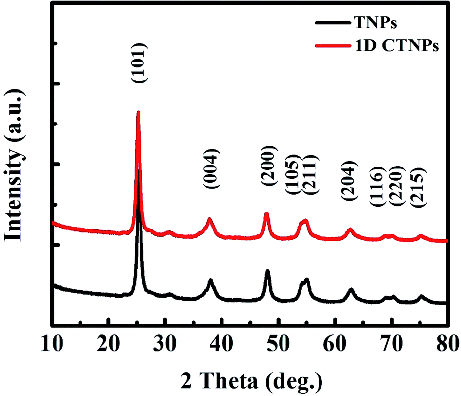
The phase structures and crystallinities of the two TiO2 samples were characterized using XRD. As shown in Fig. 2, the diffraction peaks of the two samples were indexed to the anatase phase of TiO2 (JCPDS no. 73-1764). In detail, the major peaks at 25.37°, 37.90°, 48.16°, 54.05°, 55.20°, 62.87°, 68.97°, 70.48° and 75.28° correspond to the reflections of the (101), (004), (200), (105), (211), (204), (116), (220), and (215) crystal planes of anatase TiO2, respectively. The intensities of the diffraction peaks of the anatase phase of the two samples at 25.37° were stronger than those of the other diffraction peaks, indicating that the main growth direction of the as-prepared TiO2 samples was along with (101) direction. Growth along the (101) crystal plane is advantageous for electronic applications as it results in higher electron transport speed, lower carrier recombination rate, better optical transparency, and higher specific surface area compared to growth along other directions.27
 | ||
| Fig. 2 XRD patterns of the two TiO2 powders obtained after different reaction times (10 and 30 min). | ||
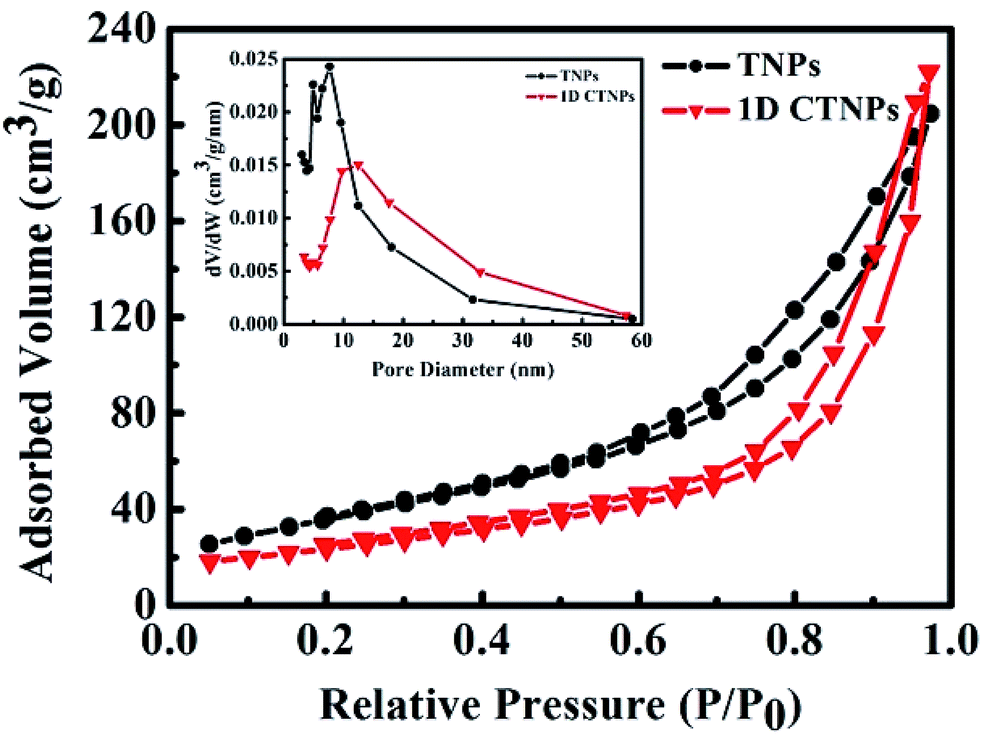
The specific surface areas and pore size distributions of the TNPs and 1D CTNPs were characterized based on nitrogen adsorption–desorption isotherms (Fig. 3). Both samples exhibited type-IV isotherms according to the Brunauer–Deming–Deming–Teller classification.28 For the TNPs, the pore size distribution (inset in Fig. 3) calculated from the desorption branch of the nitrogen isotherm by the BET method indicates a wide range of pore sizes from 5 to 60 nm with a maximum pore diameter of about 7.55 nm. For the 1D CTNPs, the pore size distribution (inset in Fig. 3) indicates a maximum pore diameter of about 12.45 nm. The ordered self-assembly of TNPs in the 1D CTNPs (see the SEM and TEM results) clearly resulted in greater pore sizes and smaller BET specific surface area (84.11 versus 111.94 m2 g−1) compared to the TNPs. Although the BET specific surface area of the 1D CTNPs was slightly lower than that of the TNPs, the large pore size distribution would be extremely useful in QDSSCs by providing pathways for colloidal QDs and electrolyte molecules.
 | ||
| Fig. 3 Nitrogen adsorption–desorption isotherms and the corresponding pore size distributions (inset) of the TNPs and 1D CTNPs. | ||
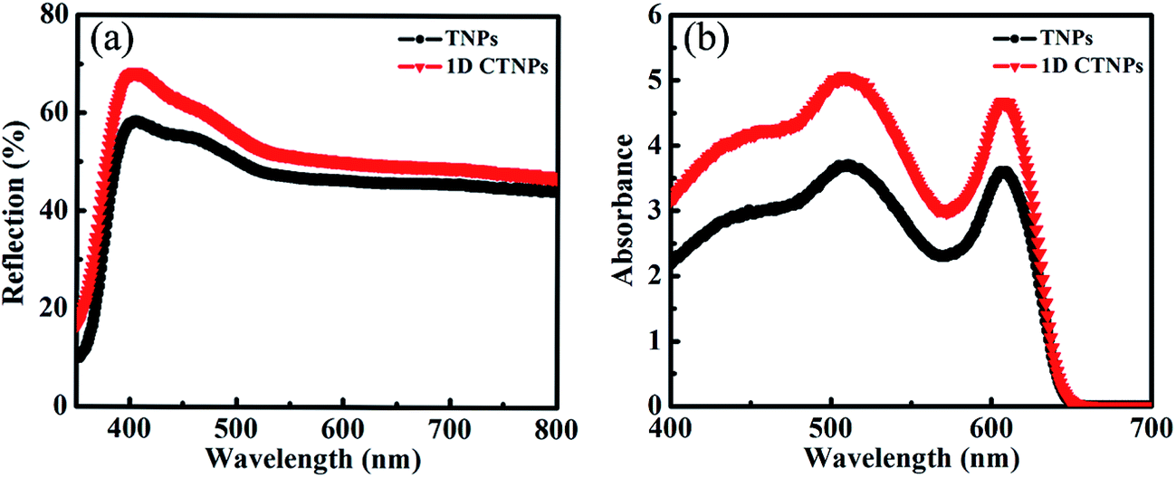
For comparison, two kinds of TiO2 photoanode films (film 1, TNPs; film 2, 1D CTNPs) with similar average thicknesses were deposited on FTO glasses coated with TiO2 barrier layers using the same screen-printing times. Fig. S1 in the ESI† shows the cross-sectional SEM images of seven TNP films and seven 1D CTNP films formed using the same screen-printing time. The film thicknesses were slightly different, and the average thickness was about 21 μm. Fig. 4 shows the cross-sectional SEM images of the photoanode films prepared using the TNP and 1D CTNP pastes. The thicknesses of the two photoanode films were similar (average thickness = 21 μm), and the TiO2 nanostructures in the photoanode films were largely retained after screen printing compared with the as-prepared TiO2 powers (as shown in Fig. 4(b) and (d)). CdSe QDSSCs based on the two films were fabricated by assembling sandwich structures with polysulfide electrolytes and Cu2S counter electrodes. Fig. 5(a) shows typical J–V curves of the two CdSe QDSSCs irradiated by AM 1.5 G simulated sunlight (100 mW cm−2). The detailed photovoltaic parameters, including Jsc, Voc, fill factor (FF), and overall PCE, are summarized in Table 1. The two CdSe QDSSCs have similar FFs of 51–52%. However, the Voc of the 1D CTNPs-based cell was higher than that of the TNP-based cell (550 versus 596 mV), and the Jsc values were significantly different (14.29 mA cm−2 for the TNP-based cell and 17.48 mA cm−2 for the 1D CTNP-based cell). As a result, the PCEs different significantly (4.00% for the TNP-based cell compared to 5.45% for the 1D CTNP-based cell). To further illustrate the effects of the TNP- and 1D CTNP-based photoanodes on the performances of the CdSe QDSSCs, the monochromatic IPCE spectra were collected as functions of wavelength from 350 to 700 nm (Fig. 5(b)). Compared with the TNP-based cell, the 1D CTNP-based cell resulted in an obvious enhancement in quantum efficiency over the entire tested wavelength range. Generally, IPCE can be defined as IPCE(λ) = LHE(λ)φinj(λ)φreg(λ)ηcc(λ), where LHE(λ) is the light-harvesting efficiency, φinj(λ) and φreg(λ) are the quantum yields for electron injection and quantum dot regeneration, respectively, and ηcc(λ) is the charge collection efficiency.29 1D CTNP-based film had a higher reflectance value than the TNP-based film over the entire wavelength range from 350 to 700 nm (Fig. 6(a)), indicating that 1D CTNPs have better light-scattering ability than TNPs.26,30–32 Fig. 6(b) shows the optical absorbances of the CdSe QD-sensitized photoanodes based on TNP and 1D CTNP films (TNPs/CdSe and 1D-CTNPs/CdSe, respectively). The absorbance of the 1D-CTNPs/CdSe film was much higher than that of TNPs/CdSe film, indicating that a greater amount of CdSe QDs was absorbed on the 1D CTNP photoanode. As shown in the inset of Fig. S2 in the ESI,† the darker color of the 1D CTNPs/CdSe film compared to the TNPs/CdSe film also implies a greater amount of adsorbed QDs. To further investigate the difference in the loading of colloidal CdSe QDs on the 1D CTNP and TNP films, the Cd/Ti atomic ratios at different depths in the TNPs/CdSe and 1D CTNPs/CdSe films are shown in Fig. S2.† Fig. S3† shows the detailed EDX images at different depths in the TNPs/CdSe and 1D CTNPs/CdSe films. The Cd/Ti atomic ratios in the 1D CTNPs/CdSe film were about 1.6-times larger than those in the TNPs/CdSe film at all depths, confirming that more QDs were adsorbed onto the 1D CTNP film than on the TNP film. LHE is mainly influenced by the light-scattering ability of the photoanode and the amount of loaded QDs. The above experimental results indicate that the LHE of the CdSe QDSSC based on 1D-CTNP was higher than that of the CdSe QDSSC based on TNPs, and this higher LHE was responsible for the enhanced Jsc. The φinj(λ) and φreg(λ) values of the TNPs/CdSe and 1D CTNPs/CdSe photoelectrodes were the same.
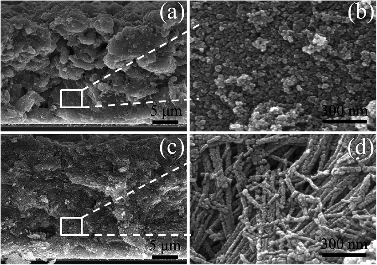 | ||
| Fig. 4 Cross-sectional SEM images of the TNPs (a and b) and 1D CTNPs (c and d) photoanode films. | ||
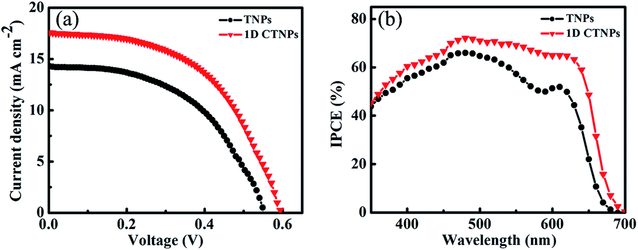 | ||
| Fig. 5 (a) J–V characteristics and (b) IPCE spectra of QDSSCs based on TNPs and 1D CTNPs films. | ||
| Cells | Jsc (mA cm−2) | Voc (mV) | FF (%) | PCE (%) |
|---|---|---|---|---|
| TNPs | 14.29 | 550 | 51 | 4.00 |
| 1D CTNPs | 17.48 | 596 | 52 | 5.45 |
 | ||
| Fig. 6 (a) Diffuse reflectance spectra of the two TiO2 films. (b) UV-visible absorption spectra of the two TiO2/CdSe films. | ||
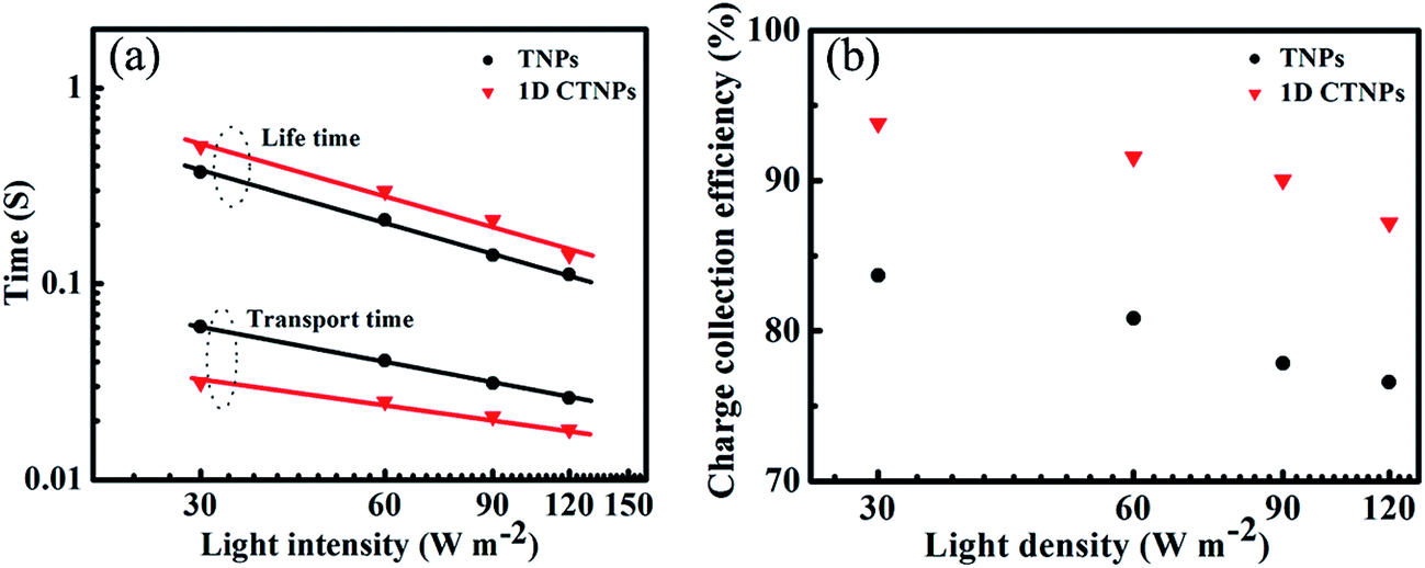
To further investigate the charge collection efficiencies [ηcc(λ)] of the two QDSSCs, IMPS and IMVS measurements were employed to characterize the dynamics of charge transport and charge recombination in the QDSSCs. The electron transport time (τd) and electron lifetime (τr) were derived from the IMPS and IMVS maps using the following expressions: τd = 1/2πfd and τr = 1/2πfr, where fd and fr are the characteristic minimum frequencies of the IMPS and IMVS imagery components, respectively.23,33 Fig. 7(a) shows the τd and τr values of the QDSSCs based on the above two photoelectrodes as functions of light intensity. Both τd and τr decreased with increasing light intensity due to the fact that at higher light intensities there are more photo-generated electrons available to fill the deep traps, and since electron trapping/detrapping occurs at shallower levels, the transfer of other free electrons becomes faster the closer to full the traps are.29 Compared with the QDSSC based on the TNP photoanode, the QDSSC based on the 1D CTNP photoanode exhibited a faster electron transport rate (lower τd) and slower electron recombination rate (larger τr). This was attributed to the fact that: compared with TNPs photoanode, self-assembly of TiO2 nanoparticle into 1D nanochains in 1D CTNPs, which provide a shorter and efficient electron transport pathway, thus leading to the faster electron transport rate, moreover, the smaller specific surface area would decrease additional recombination centers to suppress charge recombination, leading to prolonged electron lifetime. The charge collection efficiency of the QDSSCs based on the two types of TiO2 photoanodes were estimated using the following equation: ηcc = 1 − (τd/τr); the results are shown in Fig. 7(b).34 The ηcc values of the QDSSC based on the 1D CTNP photoanode were higher than those of the QDSSC based on the TNP photoanode at different incident light densities. Taking all factors into account, the higher IPCE of the 1D CTNP-based cell compared to the TNP-based cell can be rationally attributed to the enhanced light-harvesting efficiency and good charge collection efficiency of the 1D CTNP-based cell, which led to higher Jsc.
 | ||
| Fig. 7 (a) Electron lifetimes and electron transport times and (b) charge collection efficiencies of CdSe QDSSCs based on TNPs and 1D CTNPs photoanode films. | ||
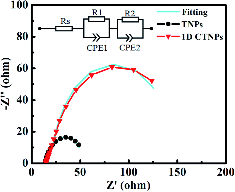
To deeply investigate the interfacial electron transfer resistance, the EIS spectra of the two cells were also collected (Fig. 8). The Nyquist curves exhibited two semicircles corresponding to electron injection at the counter electrode/electrolyte interface and transfer in the electrolyte at high frequencies (R1, the first semicircle), and recombination resistance for the electron-transfer process at the TiO2 film/QDs/electrolyte interface and transport in the TiO2 film (R2, the second semicircle).35 The fitting results show the value of R2 of 1D CTNP-based cell increases from 31.20 Ω to 124.50 Ω compared with TNPs based cell, which predicted the reduced interfacial recombination, and thus leading to higher Voc, which is in agreement with above photovoltaic data. The increase in R2 is mainly attributed to the reduction in the contact area of TiO2 with the electrolyte because the relatively low specific surface area and high loading of QDs on the 1D CTNP-based photoanode impede the direct exposure of TiO2 to the electrolyte. Meanwhile, the 1D CTNPs may be efficiently coated by the inorganic ZnS/SiO2 double barrier layer. Furthermore, Rs corresponds to the sheet resistance of the FTO glass substrate and the contact resistance at the FTO/TiO2 interface.29 The Rs values of QDSSCs based on TNP and 1D CTNP photoanodes calculated according to the equivalent circuit were similar (14.17 and 14.75 Ω), indicating that the electronic contact between two TiO2 nanostructures and FTO glass is almost the same.
 | ||
| Fig. 8 EIS spectra of CdSe QDSSCs based on TNPs and 1D CTNPs photoanode films. | ||
Having considered all the above factors, both the charge transfer resistance and light scattering capacity affect Voc and Jsc, which further directly caused change of PCE based on the QDSSCs. In short, compared with the TNP-based cell, the higher short-circuit current density of the 1D CTNP-based cell can be mainly explained by the suitable specific surface area and large pore diameter for adsorbing more CdSe QDs, prominent light-scattering capacity, which enhances the light-harvesting efficiency, and faster electron transport time and slower charge recombination rate compared to the TNP-based cell, leading to a higher Voc. Finally, an impressive PCE was obtained for the CdSe QDSSC based on the 1D CTNP photoelectrode.
4. Conclusions
In summary, novel 1D CTNPs formed by the ordered self-assembly of TNPs have been synthesized by a facile one-pot solvothermal route and used to fabricate efficient CdSe QD-sensitized solar cells. The 1D CTNP-based cell shows an impressive PCE of 5.45%, representing an ∼36% enhancement compared to the TNP-based cell. The enhanced PCE is attributed to the improvement of Jsc and Voc. The considerable improvement in the photovoltaic performance of the 1D CTNP-based cell can be attributed to enhanced light-harvesting efficiency and charge collection efficiency resulting from the fast electron transport rate and long electron lifetime. The new 1D CTNP-based photoanode is an optimal candidate for obtaining highly efficient QDSSCs.Acknowledgements
This work was supported by the National Natural Science Foundation of China (No. 61404039, 11304068); Heilongjiang Province Foundation for Returned Chinese Scholars (No. LC201401); Educational Commission of Heilongjiang Province of China (No. 12531Z006); Guangzhou Science and Technology project (No. 2016201604030047); Postdoctoral Foundation of Heilongjiang Province (301000095); and the Open Project Program of the Key Laboratory for photonic and Electric Bandgap Materials, Ministry of Education, Harbin Normal University (No. PEBM201503). The work was also supported by a grant from technology project of returned overseas students of Heilongjiang Province.References
- K. W. J. Barnham, M. Mazzer and B. Clive, Nat. Mater., 2006, 5, 161–164 CrossRef CAS.
- M. He, D. J. Zheng, M. Y. Wang, C. J. Lin and Z. Q. Lin, J. Mater. Chem. A, 2014, 2, 5994–6003 CAS.
- P. V. Kamat, K. Tvrdy, D. R. Baker and J. G. Radich, Chem. Rev., 2010, 110, 6664–6688 CrossRef CAS PubMed.
- A. J. Nozik, Phys. E, 2002, 14, 115–120 CrossRef CAS.
- P. V. Kamat, Chem. Lett., 2013, 4, 908–918 CAS.
- W. W. Yu, L. H. Qu, W. Z. Guo and X. G. Peng, Chem. Mater., 2003, 15, 2854–2860 CrossRef CAS.
- J. Wang, Y. Li, Q. Shen, T. Izuishi, Z. X. Pan, K. Zhao and X. H. Zhong, J. Mater. Chem. A, 2016, 4, 877–886 CAS.
- A. M. Smith and S. Nie, Acc. Chem. Res., 2010, 43, 190–200 CrossRef CAS PubMed.
- M. C. Beard, Chem. Lett., 2011, 2, 1282–1288 CAS.
- M. C. Hanna and A. J. Nozik, J. Appl. Phys., 2006, 100, 074510 CrossRef.
- H. J. Yun, T. Paik, B. Diroll, M. E. Edley, J. B. Baxter and C. B. Murray, ACS Appl. Mater. Interfaces, 2016, 8, 14692–14700 CAS.
- C. Chen, M. D. Ye, M. Q. Lv, C. Gong, W. X. Guo and C. J. Lin, Electrochim. Acta, 2014, 121, 175–182 CrossRef CAS.
- Z. W. Ren, J. Wang, Z. X. Pan, K. Zhao, H. Zhang, Y. Li, Y. X. Zhao, M. S. Iván, J. Bisquert and X. H. Zhong, Chem. Mater., 2015, 27, 8398–8405 CrossRef CAS.
- J. Du, Z. L. Du, J. S. Hu, Z. X. Pan, Q. Shen, J. K. Sun, D. H. Long, H. Dong, L. T. Sun, X. H. Zhong and L. J. Wan, J. Am. Chem. Soc., 2016, 138, 4201–4209 CrossRef CAS PubMed.
- N. Buatong, I. M. Tang and P. O. Weeraphat, Nanoscale Res. Lett., 2015, 10, 146 CrossRef PubMed.
- M. J. Bierman and S. Jin, Energy Environ. Sci., 2009, 2, 1050–1059 CAS.
- T. Berger, L. V. Teresa, M. S. Damián and R. Gómez, J. Phys. Chem. C, 2007, 111, 9936–9942 CAS.
- R. Ahmed, L. Zhao, A. J. Mozer, G. Will, J. Bell and H. X. Wang, J. Phys. Chem. C, 2015, 119, 2297–2307 CAS.
- X. F. Guan, S. Q. Huang, Q. X. Zhang, X. Shen, H. C. Sun, D. M. Li, Y. H. Luo, R. C. Yu and Q. B. Meng, Nanotechnology, 2011, 22, 465402 CrossRef PubMed.
- H. L. Feng, W. Q. Wu, H. S. Rao, L. B. Li, D. B. Kuang and C. Y. Su, J. Mater. Chem. A, 2015, 3, 14826–14832 CAS.
- G. S. Wang, H. Y. Wei, Y. H. Luo, H. J. Wu, D. M. Li and X. H. Zhong, J. Power Sources, 2016, 302, 266–273 CrossRef CAS.
- D. Esparza, I. Zarazúa, L. L. Tzarara, C. P. Andrea, S. S. Ana, T. C. Alejandro, M. S. Ivan and E. D. L. Rosa, J. Phys. Chem. C, 2015, 119, 13394–13403 CAS.
- H. X. Wang, P. G. Nicholson, L. Peter, S. M. Zakeeruddin and M. Gratzel, J. Phys. Chem. C, 2010, 114, 14300–14306 CAS.
- K. Zhao, Z. X. Pan, M. S. Iván, E. Cánovas, H. Wang, Y. Song, X. Q. Gong, J. Wang, M. Bonn, J. Bisquert and X. H. Zhong, J. Am. Chem. Soc., 2015, 137, 5602–5609 CrossRef CAS PubMed.
- H. Zhang, H. L. Bao and X. H. Zhong, J. Mater. Chem. A, 2015, 3, 6557–6564 CAS.
- J. Y. Liao, J. W. He, H. Y. Xu, D. B. Kuang and C. Y. Su, J. Mater. Chem., 2012, 22, 7910–7918 RSC.
- D. K. Roh, W. S. Chi, S. H. Ahn, H. Jeon and J. H. Kim, ChemSusChem, 2013, 6, 1384–1391 CrossRef CAS PubMed.
- J. G. Yu, J. J. Fan and K. L. Lv, Nanoscale, 2010, 2, 2144–2149 RSC.
- Y. F. Xu, Q. W. Wu, H. S. Rao, H. Y. Chen, D. B. Kuang and C. Y. Su, Nano Energy, 2015, 11, 621–630 CrossRef CAS.
- Q. W. Wu, H. S. Rao, H. L. Feng, H. Y. Chen, D. B. Kuang and C. Y. Su, Nano Energy, 2014, 9, 15–24 CrossRef.
- Q. W. Wu, H. S. Rao, Y. F. Xu, Y. F. Wang, C. Y. Su and D. B. Kuang, Sci. Rep., 2013, 3, 1892 Search PubMed.
- J. Y. Liao, B. X. Lei, D. B. Kuang and Y. C. Su, Energy Environ. Sci., 2011, 4, 4079–4085 CAS.
- L. Dloczik, O. Ileperuma, I. Lauermann, L. M. Peter, E. A. Ponomarev, G. Redmond, N. J. Shaw and I. Uhlendorf, J. Phys. Chem. B, 1997, 101, 10281–10289 CrossRef CAS.
- H. S. Rao, Q. W. Wu, Y. Liu, Y. F. Xu, B. X. Chen, H. Y. Chen, D. B. Kuang and C. Y. Su, Nano Energy, 2014, 8, 1–8 CrossRef CAS.
- J. Y. Liao, H. P. Lin, H. Y. Chen, D. B. Kuang and C. Y. Su, J. Mater. Chem., 2012, 22, 1627–1633 RSC.
Footnote |
| † Electronic supplementary information (ESI) available. See DOI: 10.1039/c6ra26029b |
| This journal is © The Royal Society of Chemistry 2017 |