
 Open Access Article
 This Open Access Article is licensed under a
 Creative Commons Attribution 3.0 Unported Licence
A flexible conductive film prepared by the oriented stacking of Ag and Au/Ag alloy nanoplates and its chemically roughened surface for explosive SERS detection and cell adhesion†
Mingming Suna,
Hongmei Qianb,
Jia Liua,
Yuchuan Lia,
Siping Panga,
Meng Xu*a and
Jiatao Zhang *a
*a
aBeijing Key Laboratory of Construction Tailorable Advanced Functional Materials and Green Applications, School of Materials Science & Engineering, Beijing Institute of Technology, Beijing, 10081, P. R. China. E-mail: xumeng@bit.edu.cn; zhangjt@bit.edu.cn
bDepartment of Architecture and Civil Engineering, West Anhui University, Liuan, 237012, P. R. China
First published on 20th January 2017
Abstract
A large-scale assembly of nanostructured building blocks into bulk flexible film with multifunctional applications is the key point in colloidal nanomaterials research. In this study, a centimeter-scale flexible conductive film was prepared by the oriented stacking of Ag nanoplates on a polyethylene glycol terephthalate (PET) flexible substrate and it displayed an ideal ohmic contact and low resistance (112 Ω cm−1). Via a solid–liquid interface galvanic replacement reaction with HAuCl4, a Au–Ag alloy nanoplate film was obtained with an enhanced conductivity (10.2 Ω cm−1) and controllable surface roughness. The optimized surface roughness of this flexible conductive film enabled the ultrasensitive surface-enhanced Raman spectroscopy (SERS) detection of explosives (TNT and RDX) and their differentiation at low concentrations (10 nM). Moreover, the synergistic nanoscale and microscale surface roughness of this Au–Ag alloy nanoplate film endowed good biocompatibility and demonstrated applicable biological cell adhesion performance.
Introduction
The exploration of nanometer-sized building blocks towards multifunctional films requires not only the tunable size and shape of the building blocks, but also their large-scale assembly on a flexible substrate with multifunctional performance. The latter is increasingly important from the perspective of exploiting the collective properties, such as flexible conductivity, sensing, biological, and so forth, of nanocrystal assemblies for practical applications.1–4 Therefore, multifunctional large area noble metal nanoparticle assemblies (NPAs) have attracted significant interest. To achieve the electrical conductivities of NPAs close to that of bulk noble metal for electronics applications, many methods have been used, such as self-assembly of colloidal nanoparticles using linker molecules or increasing the nanocrystal coverage via a reduction process.5,6 Most of these studies have focused on the fabrication of NPAs films on a rigid substrate.7–11 The fabrication of conductive multifunctional NPAs film on a flexible substrate is an important aspect for portable devices and biocompatible applications.12 The distance between adjacent nanocrystals (NCs) and the contact of the NCs to the substrate are the key issues to achieve these NPAs-constructed flexible conductive films.13 Some attempts have been made to improve the conductivity of NPAs;14,15 for example, Xia, Li and Ray et al. have respectively reported the synthesis of Au–Ag alloy nanostructures via a galvanic replacement reaction between gold chloride and silver nanoparticles.16–21 Furthermore, because the surface roughness of NPAs enables electromagnetic filed enhancement,22 they can also be used in the surface-enhanced Raman scattering (SERS) applications. Although some SERS substrates composed of noble metal NPs have been reported, the production of large-area NPAs with controllable roughness to obtain improved EM enhancement is still far from real applications.23–27 Moreover, there is an increasing demand for versatile SERS detection, such as applications towards various kinds of analytes including explosive organics, which affect the safety of human beings.4,28Metal nanoparticles have potential applications for the treatment of cancer cells. Cancer cells have significant responses to an extracellular environment in the nanometer scale. Environment would affect cell migration and metastasis through the transfer of mechanical signals from the materials surface to the biochemicals.29,30 Yang et al. have demonstrated that Si nanowires with a high aspect ratio are accessible to living cells. Li et al. reported that a GaN nanowire substrate can be used for cell capture.31–33 Herein, the galvanic replacement reaction mechanism was used to modify the surface roughness and remove the surface organic protection layer of Au–Ag alloy nanoplate films on a flexible substrate. The roughened surface of a Au–Ag alloy nanoplate film was exploited to capture cancer cells with enhanced efficiency.
In this study, the facile formation of a large area (centimeter scale) film was realized via oriented stacking of Ag nanoplates on a flexible polymer, polyethylene glycol terephthalate (PET), substrate. The controlled solid–liquid interface galvanic replacement reaction between HAuCl4 solution and flexible Ag nanoplate film was utilized to remove the organic capping layer between the nanoplates to obtain improved conductivity and at the same time to roughen the nanoplate surface for enhancing the SERS signal. The obtained Au–Ag alloy nanoplate film on a flexible substrate has a stable conductivity even under strong bending. We also studied NIH 3T3 cell capture on the Au–Ag alloy nanoplate substrate; the well-extended morphologies of the objective cells on the substrate suggest their good biological application potential.
Experimental section
Synthesis and suspension of Ag nanoplates
The synthesis of single-crystalline Ag nanoplates was conducted following the previously reported procedures.19,34,35 Typically, 5.5 g of PVP was dissolved in 25 mL of DMF in an autoclave. Then, 0.172 g of AgNO3 was added to the mixture under intense stirring to obtain a clear colloid and the mixture was kept at 150 °C for 12 hours. After this, the silver nanoplates were formed and were washed with ethanol. The final sample was redispersed with a small amount of 18.2 MΩ cm ultrapure water (Hitech-Sciencetool) at a concentration of 4 mg mL−1.Preparation and characterization of the large-scale assembly of the Ag nanoplates on the PET film
The PET film was sheared into a square of 4 cm in length. It was washed with acetone and dipped in 3-aminopropyl methyl dimethoxy silane for 1 hour to achieve a hydrophilic surface. Then, the film was washed with ethanol and dried in air. The as-prepared Ag nanoplates colloid was dropped onto the film and aged for 12 hours in a vacuum oven at 65 °C. To obtain the corresponding X-ray diffraction pattern of Ag, the as-prepared Ag solution was also dropped onto a silica slide. The XRD pattern was obtained using a Bruker D8 Advance X-ray powder diffractometer with Cu Kα radiation (λ = 1.5418 Å). The morphology of Ag was examined via SEM using a Hitachi FE-SEM 4800 instrument and TEM using a JEOL JEM-1200EX instrument working at 100 kV.The conductive and mechanical property measurements of the as-prepared Ag nanoplate film on the PET surface
Before the conductivity test, flexible PET films with Ag nanoplate assemblies were bent 50 times at different degrees. One probe was attached to the PET film surface with no Ag nanoplates present, whereas the other probe was contacted to the Ag nanoplate film. The return circuit was achieved after completion of the abovementioned process. The distance of the probes was confirmed at 1 cm. By varying the voltage from −1 V to 1 V for a pure Ag conductive film (the voltage from −10 mV to 10 mV for the Au–Ag alloy conductive film), the current constantly changed when investigated at room temperature.In situ conversion of the Ag nanoplate film to a Au–Ag alloy nanoplate film on the substrate
The Ag nanoplate film on a PET substrate was dipped in a 15 mL of PVP aqueous solution (2 mg mL−1). Then, 10 mL of a HAuCl4 solution (0.2 mM mL−1) was added dropwise to the abovementioned mixture. The reaction occurred in a 50 mL flask at 100 °C. After being reacted for 30 minutes, the as-obtained film samples were washed three times with ethanol. After the in situ conversion, a silica slide was pressed on the Au–Ag alloy surface to prepare the sample for XRD measurement. The morphology of the Au–Ag alloy nanoplates was also examined via SEM. The EDS line profiles, elemental mapping analyses, and STEM image of the Au–Ag alloy nanoplates were obtained using a high-resolution TEM (FEI Tecnai G2 F20 S-Twin working at 200 kV) to confirm the elements in the Au–Ag nanoplates. Three-dimensional (3D) and 2D atomic force microscopy (AFM) was used to study the roughness of the Ag and Au–Ag alloy nanoplates. Tapping-mode AFM studies were performed using a Dimension 3100 AFM (Bruker, USA) under ambient conditions. Commercial silicon tips with a nominal spring constant of 2.0 N m−1 and resonant frequency of 437.2 kHz were used in all the AFM imaging studies.SERS detection of explosives using the as-prepared Au–Ag alloy nanoplate film
The commonly used explosive molecules TNT (trinitrotoluene) and RDX (cyclotrimethylenetrinitramine) were chosen as analytes. TNT and RDX were respectively dissolved in acetone (10 nM) and the as-obtained explosive solutions were sealed in the dark. The Au–Ag alloy nanoplate film with a size of 0.5 cm was employed as the SERS substrate. The explosive solutions (15 μL) were added to the substrate and dried by natural evaporation. The freshly prepared sample was analyzed by Raman spectroscopy. The SERS spectra were obtained via a microscopic confocal Raman spectrometer (Renishaw inVia) using a laser beam with an excitation wavelength of 633 nm and a charge coupled device (CCD) detector with a resolution of 4 cm−1. The power was maintained at 0.5 mW to avoid the destruction of the samples. The pure TNT and RDX solutions were tested on a silica slide. The explosive solutions were also tested on the Ag nanoplate substrate. All the explosive solutions used in this study had the same concentration. The preparation and characterization of the as-prepared Au–Ag alloy nanoplate film were carried out in the same manner as that for the Ag conductive film.Cell culture on the Au–Ag alloy on a PET surface and cell test using fluorescence microscopy and SEM
NIH 3T3 cells (obtained from the Chinese academy of medical science & Peking union medical college) were cultured in DMEM medium (Hyclone) containing 100 μg mL−1 streptomycin, 1% glutamine, 100 IU mL−1 penicillin, and 10% (v/v) heat-inactivated calf serum (Gibco). Cells were cultured in Au–Ag and pure Ag substrates, which were placed into 24-well plates. The culture plates were placed in the incubator at 37 °C in a 5% CO2 atmosphere. The NIH 3T3 cells were cultured for 48 hours. Before being tested using fluorescence microscopy (Leica, Germany) at an excitation wavelength of 488 nm and pass filter of 515 nm, the cells were dyed using acridine orange and washed three times with PBS solution. Prior to SEM (Hitachi FE-SEM 4800) measurement, the cells were fixed using glutaraldehyde (2.5% dispersed in PBS solution), dehydrated with a gradient of ethanol, and dried using a critical point drying (CPD) method.Results and discussion
The as-prepared Ag nanoplates are facile to assemble on a large scale based on stacking, as indicated by Fig. 1a and b. The stacking morphology of the Ag nanoplates with metallic Lustre was proven, as shown in Fig. S1.† The thin nanoplates with micrometer size can be affected by a twisting force, which contributes to the metallic Lustre. It can be seen that the surface of each individual Ag nanoplate was very smooth. The Ag film was composed of several stacked layers of Ag nanoplates even though not in a close-packing pattern. This multiple stack avails substantial attachment to make a passage for charge transport. Fig. 1c shows the corresponding XRD pattern of the pure Ag nanoplates, from which it can be observed that the as-prepared silver nanoplates are single crystals with a face-centered-cubic (fcc) structure. The dominant (111) peak suggests that the silver nanoplates are tiled on the substrate because of the action of gravity. The weak diffraction peak of the (200) plane was also discerned from the XRD pattern. The inset in Fig. 1a illustrates that different layers of Ag nanoplates are oriented via stacking rather than via simple duplication. The natural dislocation of the Ag nanoplates can reduce the plate-to-plate junction resistance and improve the film conductance.36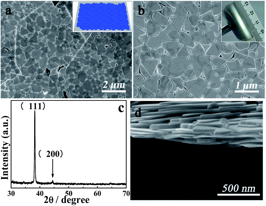 | ||
| Fig. 1 (a and b) SEM images of Ag nanoplates assembly on the PET film at different magnifications. The inset image in (a) is a schematic of the assembled Ag nanoplates on PET. The inset image in (b) shows the centimetre scale Ag nanoplate film formed on the flexible PET substrate. (c) XRD pattern of the Ag nanoplates. (d) The SEM image of the cross-section of the Ag nanoplate film. | ||
The inset in Fig. 1b displays the good flexibility of the macroscopic assembly product. Fig. 1d is the section image of the stack of Ag nanoplates. All of these Ag nanoplates contact with the neighbouring nanoplates by the (111) facet to increase the stability. The thickness of the Ag nanoplate film can be regulated by changing the amount of Ag solution, which is convenient for ultra-thin electronic devices. Note that the PET surface was modified with 3-aminopropyl methyl dimethoxy silane to assist in the attachment between the Ag nanoplates and PET, considering that only strong contact between the bottom nanoplate layer and PET can facilitate the formation of Ag films with good morphology and conductivity for further applications.
With the use of PVP as a protecting ligand, AuCl4− can selectively corrode the (111) plane of the Ag nanoplates resulting in the desired coarse facets.16,19,37,38 Fig. 2a schematically illustrates the galvanic reaction-enabled transformation from smooth-surfaced nanoplates to rough-surfaced nanoplates. This is an in situ conversion process that hardly disturbs the original position of the individual nanoplates assembled on the PET film and therefore is able to inherit the desirable architecture from the Ag assembly film towards the creation of an advanced SERS substrate.
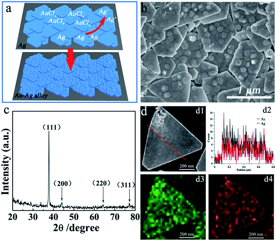 | ||
| Fig. 2 (a) A schematic of the solid–liquid interface galvanic replacement reaction between the Ag nanoplate film and HAuCl4 solution. The resulting Au–Ag alloy possesses a rough surface after the in situ conversion. (b) The SEM image of the Au–Ag alloy nanoplates on the transparent PET film after the in situ conversion. (c) The XRD pattern of the Au–Ag alloy nanoplate film. (d) Dark-field scanning transmission electron microscopy (STEM) image (d1), line scanning (d2) and elemental mapping for Ag (d3) and Au (d4) elements of the surface roughened Au–Ag alloy nanoplate. | ||
Characterization of the morphology of the Au–Ag alloy is provided in Fig. 2b and S1,† from which it can be observed that the surfaces of the Au–Ag nanoplates are full with hollows and bulges, as presented in Fig. 2a. The well-maintained outlines of the nanoplates may favor the complete dipole resonance and quadrupole resonance from the edges, which is important for achieving E-field enhancement and accordingly, enhanced SERS signals. As shown in the XRD pattern, in Fig. 1c, only one sharp diffraction peak, corresponding to the Ag {111} facets (JCPDS No. 04-0783), appeared in the spectrum of the as-prepared single-crystalline Ag nanoplates because of the large exposure of these facets. After reacting with AuCl4−, the diffraction peaks of the (200), (220), and (311) Au–Ag alloy facets were observed (JCPDS No. 65-8464),39–41 as shown in Fig. 2c. The strong (111) diffraction peak revealed that the (111) plane still dominates the exposed facet of the nanoplates. Furthermore, the energy dispersive spectroscopy (EDS) line profiles and elemental mapping analyses of the Au–Ag alloy nanoplates revealed that both Au and Ag atoms were homogeneously distributed in the nanostructures, which further confirms the alloyed state of the Au and Ag atoms in the as-prepared Au–Ag nanoplates. Moreover, we can tune the surface roughness of the Au–Ag alloy with different amounts of HAuCl4; as shown in Fig. S2,† the roughness of the Au–Ag alloy was enhanced upon increasing the amount of HAuCl4. The quantitative analysis data for the controlled roughness was studied via atomic force microscopy (AFM), as shown in Fig. S3.† Although phase conversion probably occurs on the outside of the nanoplates with limited depth, it is considered to be sufficient with respect to SERS applications.
The horizontal direction resistance of the Ag film was tested using the method shown in the inset image of Fig. 3a. The obtained I–V curve, as shown in Fig. 3a, which is denoted as Line 1, is a straight line with an original resistance of approximately 112 Ω cm−1 (Table S1†). To detect the resistance stability of the Ag film, we bent the film at four different bending degrees and obtained the corresponding I–V curves after its recovery from bending. The bending degree is defined as L/L0, where L0 represents the initial length of the Ag film and L is the length of the film under a bending force, as illustrated in Fig. 3a. For each bending degree, the bending operation over the soft Ag film was performed 50 times. The obtained I–V curves are denoted as Line 2–5 in Fig. 3a, and the corresponding bending degrees and resistance values are shown in the ESI (Table S1†). After subjecting the Ag film to different degrees of bending, the I–V curves displayed no obvious changes and each line was linear, indicating high resistance stability. The minor changes in the average resistance, which were probably caused by environmental factors, evidence the retention of the good attachment of the Ag nanoplates to their neighbours. Moreover, the low resistance values imply that each layer of the assembled silver nanoplates stay in good contact with the neighbouring layers. The resistance of the Au–Ag alloy nanoplate film was tested using the same method as that used for the Ag nanoplate film. The straight Line 1 in Fig. 3b belongs to the original I–V curve of the Au–Ag alloy nanoplate film, which has a higher conductivity than the Ag nanoplates assembly. The original resistance was approximately 10.3 Ω cm−1 (Table S2†). Line 2–4 are the Au–Ag alloy I–V curves obtained from four different bending degrees. All of the I–V curves are straight lines, which are evidence of the stable conductivity of the Au–Ag alloy. The resistance fluctuation of the Au–Ag alloy is weaker than that of the pure Ag assembly film, which perhaps originates from the higher conductivity. The average resistance of Line 1–5 of the Au–Ag alloy nanoplate film was 10.2 Ω cm−1, whereas that of the pure Ag nanoplate film was 112 Ω cm−1. AuCl4− ions enhance the conductivity of the neighbouring Ag layers via the galvanic reaction. The in situ conversion generates many spots on the Ag nanoplates surfaces, which result in the improved connection of the neighbouring Ag layers. Moreover, the most organic ligands are replaced by AuCl4− ions after the galvanic reaction, which improves the conductivity of the Au–Ag alloy film. The abovementioned results strongly suggest the possibility of the flexible Ag and Au–Ag alloy nanoplate-assembled films to be used for flexible electronic devices applications. The unique architecture of the Ag and Au–Ag alloy nanoplate film is considered to be important, which requires only a slight shift of the individual Ag nanoplates to adapt the bent substrate and allows the retention of the close contact between different nanoplate layers even during the large-angle bending tests (Fig. 3a).
 | ||
| Fig. 3 (a) The I–V curves corresponding to different bending degrees of the pure Ag assembly conductive film. The inset images are the I–V test model and a simple illustration of the bending of the Ag nanoplates on PET. (b) The I–V curves corresponding to different bending degrees of the Au–Ag alloy nanoplates conductive film. | ||
The Au–Ag alloy nanoplates with rough surfaces are favourable to gaining an increased Raman intensity for the detection of TNT and RDX (Fig. 4). The vibrational signatures of TNT and RDX were achieved by SERS with the use of the Au–Ag alloy substrate. The peak at 1205 cm−1 was ascribed to the phenylmethyl group in TNT. The peak observed at 854 cm−1 corresponds to the nitrophenyl group of the TNT molecule. It is clear that these two peaks are absent in the case of RDX. Moreover, the peak at 1290 cm−1 was ascribed to the nitramine group of RDX, which does not appear in the SERS spectrum of TNT.42 The strong symmetric nitro stretching was typically observed at 1386 cm−1. The peak at 1241 cm−1 was ascribed to the ring breathing bending. When compared with the normal SERS of TNT (symmetric nitro stretch peak at 1360 cm−1, ring breathing bending peak at 1210 cm−1), these two peaks are slightly shifted to a higher wavenumber because of the chemical adsorption between the Au–Ag alloy surface and explosive molecules. Moreover, the symmetric ring breathing peak is located at 1001 cm−1.43–45 In stark contrast, no obvious SERS signals were obtained when using the smooth-surfaced Ag assembly film as the substrate (Fig. 4), demonstrating that the Au–Ag alloy substrate with rough surfaces can intrigue improved SERS signals. Furthermore, the concentration-dependent SERS results are shown in Fig. S4.† When compared with the intrinsic Raman spectra of TNT and RDX,46 the SERS results of TNT and RDX are distinct for these two molecules at low concentrations. The TNT and RDX solutions were also dropped on a silica slide to perform the SERS measurement and no signals were observed (Fig. 4).
 | ||
| Fig. 4 The SERS spectra of TNT and RDX on the Au–Ag alloy film substrate (red and black, respectively), the Ag film substrate (purple and dark yellow, respectively), and silica slide (green and blue, respectively). | ||
In the cell experiment, the Au–Ag alloy nanoplates with many concave and convex edges on the surfaces show good adhesion for NIH 3T3 cells. The cells on the Au–Ag alloy exhibit extended flat morphologies with vimineous filopodia. As observed in Fig. 5a and b, these cells have very luminous nucleus parts and light-colored parts around the nuclei. The dimensions of the cells are several micrometers. However, cells on the pure Ag substrate exhibit round morphologies (Fig. S5†) without vimineous filopodia. Cell adhesion, metastasis, multiplication, and differentiation on the material surface are generally dependent on the cell-extracellular matrix (ECM). The ECM is composed of proteins and polysaccharides with different nanometer length scales. The rough surfaces of the Au–Ag alloy substrate, with various concave and convex edges, make it possible for a facile reaction to occur between the cell and substrate surfaces. The SEM image in Fig. 5c shows that the NIH 3T3 cell has good contact with the rough surface of the Au–Ag alloy substrate. Additionally, it can be seen that the cell has filopodia and it spreads on the alloy surface. The fluorescence microscopy images of the NIH 3T3 cells on the random-oriented Ag and Au–Ag nanoplates (Fig. S6†) show that the cells on the random-oriented stacking films have round morphologies. However, on the oriented stacking film, the cells exhibited more-extended morphologies, which indicates that the oriented stacking film has a favorable impact on the adhesion behavior of cells. The flexible Au–Ag alloy nanoplates-assembled film with excellent cytocompatibility is a viable candidate material for use as a vascular scaffold and tissue engineering substrate. Moreover, the high conductivity ensures that the film can be used as a substrate to study the response of nerve cells to electrical stimuli.
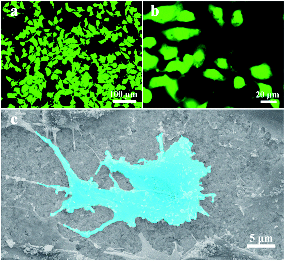 | ||
| Fig. 5 (a and b) The fluorescence microscopy images of NIH 3T3 cells cultured on the Au–Ag alloy substrate. (c) The SEM image of NIH 3T3 cells cultured on the Au–Ag alloy substrate for 48 hours. The blue pattern shows the cells with filopodia. | ||
Conclusions
Stable and smooth-surfaced Ag films were fabricated based on the assembly of Ag nanoplates on flexible PET films. The obtained Ag films were composed of several layers of Ag nanoplates and have been demonstrated to exhibit stable resistance and electrical properties. More importantly, the Ag films can be easily converted in situ into a Au–Ag alloy film with well-preserved assembly structures, enhanced conductivity even under bending (10.2 Ω cm−1), and rough-surfaced morphologies via a controlled solid–liquid interface galvanic replacement reaction. Using the Au–Ag alloy film as the substrate, strong and clear SERS signals were obtained in detecting low concentrations of TNT and RDX explosives, which cannot be realized using pure Ag films substrate. Moreover, the rough surfaces of the Au–Ag alloy films favor a significantly enhanced attachment to NIH 3T3 cells as testified by fluorescence microscopy and SEM characterization. These soft and flexible Au–Ag alloy films are envisioned to have extensive applications in molecular detection and biomedical sciences.Acknowledgements
This work was supported by the National Natural Science Foundation of China (Grant No. 21322105, 91323301, 51631001, 51372025, and 51501010). We thank Prof. Chen Wang and Prof. Yanliang Yang for their helpful discussion and assistance in the cell experiments.Notes and references
- S. Ho Jung, J. Jeon, H. Kim, J. Jaworski and J. H. Jung, J. Am. Chem. Soc., 2014, 136, 6446–6452 CrossRef PubMed.
- L. Malassis, D. Jishkariani, C. B. Murray and B. Donnio, Nanoscale, 2016, 8, 13192–13198 RSC.
- W. Niu, S. Zheng, D. Wang, X. Liu, H. Li, S. Han, J. Chen, Z. Tang and G. Xu, J. Am. Chem. Soc., 2009, 131, 697–703 CrossRef CAS PubMed.
- S. S. R. Dasary, A. K. Singh, D. Senapati, H. Yu and P. C. Ray, J. Am. Chem. Soc., 2009, 131, 13086–13812 CrossRef PubMed.
- J. Henzie, M. Grünwald, A. W. Cooper, P. L. Geissler and P. Yang, Nat. Mater., 2012, 11, 131–137 CrossRef CAS PubMed.
- S. G. Graña, J. P. Juste, R. A. A. Puebla, A. G. Martínez and L. M. Liz-Marzán, Adv. Opt. Mater., 2013, 1, 477–481 CrossRef.
- Z. Liu, L. Cheng, L. Zhang, C. Jing, X. Shi, Z. Yang, Y. Long and J. Fang, Nanoscale, 2014, 6, 2567–2572 RSC.
- Q. Cao, K. Yuan, Q. Liu, C. Liang, X. Wang, Y.-F. Cheng, Q. Li, M. Wang and R. Che, ACS Appl. Mater. Interfaces, 2015, 7, 18491–18500 CAS.
- Y. Sun, Adv. Funct. Mater., 2010, 20, 3646–3657 CrossRef CAS.
- S. Schlücker, Angew. Chem., Int. Ed., 2014, 53, 4756–4795 CrossRef PubMed.
- M. J. Mulvihill, X. Y. Ling, J. Henzie and P. Yang, J. Am. Chem. Soc., 2010, 132, 268–274 CrossRef CAS PubMed.
- D. Y. Choi, Y. S. Oh, D. Han, S. Yoo, H. J. Sung and S. S. Kim, Adv. Funct. Mater., 2015, 25, 3888–3898 CrossRef CAS.
- A. Nag, D. S. Chung, D. S. Dolzhnikov, N. M. Dimitrijevic, S. Chattopadhyay, T. Shibata and D. V. Talapin, J. Am. Chem. Soc., 2012, 134, 13604–13615 CrossRef CAS PubMed.
- C. Farcau, H. Moreira, B. Viallet, J. Grisolia and L. Ressier, ACS Nano, 2010, 12, 7275–7282 CrossRef PubMed.
- A. Tao, P. Sinsermsuksakul and P. Yang, Nat. Nanotechnol., 2007, 2, 435–440 CrossRef CAS PubMed.
- X. Lu, L. Au, J. McLellan, Z.-Y. Li, M. Marquez and Y. Xia, Nano Lett., 2007, 7, 1764–1769 CrossRef CAS PubMed.
- R. Kanchanapally, S. Sekhar Sinha, Z. Fan, M. Dubey, E. Zakar and P. C. Ray, J. Phys. Chem. C, 2014, 118, 7070–7075 CAS.
- X. Hong, D. Wang, S. Cai, H. Rong and Y. Li, J. Am. Chem. Soc., 2012, 134, 18165–18168 CrossRef CAS PubMed.
- H. Qian, M. Xu, X. Li, M. Ji, L. Cheng, A. Shoaib, J. Liu, L. Jiang, H. Zhu and J. Zhang, Nano Res., 2016, 9, 876–885 CrossRef CAS.
- E. Panfiloval, A. Shirokov, B. Khlebtsov, L. Matora and N. Khlebtsov, Nano Res., 2012, 5, 124–134 CrossRef.
- L. Au, Y. Chen, F. Zhou, P. H. C. Camargo, B. Lim, Z.-Y. Li, D. S. Ginger and Y. Xia, Nano Res., 2008, 1, 441–449 CrossRef CAS PubMed.
- S. L. Kleinman, R. R. Frontier, A.-I. Henry, J. A. Dieringer and R. P. Van Duyne, Phys. Chem. Chem. Phys., 2013, 15, 21–36 RSC.
- H.-Y. Chen, M.-H. Lin, C.-Y. Wang, Y.-M. Chang and S. Gwo, J. Am. Chem. Soc., 2015, 137, 13698–13705 CrossRef CAS PubMed.
- D. Graham, D. G. Thompson, W. Ewen Smith and K. Faulds, Nat. Nanotechnol., 2008, 3, 548–551 CrossRef CAS PubMed.
- H. Tang, G. Meng, Z. Li, C. Zhu, Z. Huang, Z. Wang and F. Li, Nano Res., 2015, 8, 2261–2270 CrossRef CAS.
- C. Duan, B. Ren, H. Liu, Y. Wang and Y. Chen, Sci. China Mater., 2016, 59, 435–443 CrossRef.
- M. Wang, G. Meng, Q. Huang, H. Tang, Z. Li and Z. Zhang, Sci. China Mater., 2015, 58, 198–203 CrossRef CAS.
- Y. Sun, K. Liu and K. Jiang, Nano Lett., 2010, 10, 1747–1753 CrossRef CAS PubMed.
- J. Meng, P. Zhang, F. Zhang, H. Liu, J. Fan, X. Liu, G. Yang, L. Jiang and S. Wang, ACS Nano, 2015, 9, 9284–9291 CrossRef CAS PubMed.
- H. Liu, Y. Li, K. Sun, J. Fan, P. Zhang, J. Meng, S. Wang and L. Jiang, J. Am. Chem. Soc., 2013, 135, 7603–7609 CrossRef CAS PubMed.
- P. P. Girard, E. A. Cavalcanti-Adam, R. Kemkemer and J. P. Spatz, Soft Matter, 2007, 3, 307–326 RSC.
- W. Kim, J. K. Ng and P. Yang, J. Am. Chem. Soc., 2007, 129, 7228–7229 CrossRef CAS PubMed.
- J. Li, Q. Han and C. Wang, ACS Appl. Mater. Interfaces, 2013, 5, 9816–9822 CAS.
- I. Washio, Y. Xiong, Y. Yin and Y. Xia, Adv. Mater., 2006, 18, 1745–1749 CrossRef CAS.
- X. He, X. Zhao, Y. Li and X. Su, J. Mater. Res., 2009, 24, 2200–2209 CrossRef CAS.
- L. Hu, H. Sun Kim, J.-Y. Lee, P. Peumans and Y. Cui, ACS Nano, 2010, 4, 2955–2963 CrossRef CAS PubMed.
- J. Zhang, X. Li, X. Sun and Y. Li, J. Phys. Chem. B, 2005, 109, 12544–12548 CrossRef CAS PubMed.
- Q. Zhang, Y. Hu, S. Guo, J. Goebl and Y. Yin, Nano Lett., 2010, 10, 5037–5042 CrossRef CAS PubMed.
- Y. Sun, B. T. Mayers and Y. Xia, Nano Lett., 2002, 2, 481–485 CrossRef CAS.
- Y. Sun and Y. Xia, Science, 2002, 298, 2176–2179 CrossRef CAS PubMed.
- J. Zhang, X. Li, X. Sun and Y. Li, J. Phys. Chem. B, 2005, 109, 12544–12548 CrossRef CAS PubMed.
- J. A. Dean, Lange's Handbook of Chemistry, 15th edn, 1999 Search PubMed.
- C. Zhang, K. Wang, D. Han and Q. Pang, Spectrochim. Acta, Part A, 2014, 122, 387–391 CrossRef CAS PubMed.
- B. D. Piorek, S. Joon Lee, M. Moskovits and C. D. Meinhart, Anal. Chem., 2012, 84, 9700–9705 CrossRef CAS PubMed.
- A. Mathew, P. R. Sajanlal and T. Pradeep, Angew. Chem., Int. Ed., 2012, 51, 9596–9600 CrossRef CAS PubMed.
- J. C. Carter, S. M. Angel and M. Lawrencesnyder, Appl. Spectrosc., 2005, 59, 769–775 CrossRef CAS PubMed.
Footnote |
| † Electronic supplementary information (ESI) available: Related synthetic details, SEM images, TEM images, fluorescence microscopy image measurement results. See DOI: 10.1039/c6ra25956a |
| This journal is © The Royal Society of Chemistry 2017 |