
 Open Access Article
 This Open Access Article is licensed under a
 Creative Commons Attribution 3.0 Unported Licence
Adjusting the band structure and defects of ZnO quantum dots via tin doping†
Weimin Yang ab,
Bing Zhangab,
Qitu Zhang*ab,
Lixi Wangab,
Bo Songc,
Yong Dingc and
C. P. Wongcd
ab,
Bing Zhangab,
Qitu Zhang*ab,
Lixi Wangab,
Bo Songc,
Yong Dingc and
C. P. Wongcd
aCollege of Materials Science and Engineering, Nanjing Tech University, Nanjing 210009, China. E-mail: ngdzqt@163.com
bJiangsu Collaborative Innovation Center for Advanced Inorganic Function Composites, Nanjing Tech University, Nanjing 210009, China
cSchool of Materials Science and Engineering, Georgia Institute of Technology, 771 Ferst Drive, Atlanta, GA 30332, USA
dFaculty of Engineering, The Chinese University of Hong Kong, Shatin 999077, Hong Kong, China
First published on 14th February 2017
Abstract
The structures and band structures of Sn doped ZnO were investigated by density functional theory (DFT). Sn-doped ZnO quantum dots were also synthesized via an ultrasonic sol–gel method. The charge of Sn ions was also taken into consideration and Sn2+ and Sn4+ were employed. UV-Vis absorption spectra and photoluminescence excitation spectra were used to elucidate the band gap of Sn-doped ZnO QDs. Photoluminescence spectra were employed to study the change in the defects of Sn-doped ZnO QDs. Sn doping reduced the symmetry of the ZnO cell and stretched the cell. Furthermore, it also could change ZnO from a direct gap semiconductor to an indirect gap semiconductor. The experimental results and DFT calculations matched quite well. Both the DFT calculations and experimental results showed that with an increasing Sn content, the band gap of Sn-doped ZnO first decreased and then increased, whereas the band gap of the ZnO base only increased. Sn doping also changed the optical defects of the quantum dots from  defects to OZn and Oi defects.
Introduction
Zinc oxide (ZnO) is a wide band gap (3.37 eV) semiconductor with a large exciton binding energy (60 meV).1,2 ZnO exhibited excellent UV-absorption and photoluminescence properties. Furthermore, ZnO is a non-toxic material and abundant in nature.Colloidal quantum dots (QDs) have attracted much attention in recent years due to their amazing characteristics in optics. There are several ways to change the energy gap of QDs. The first way is to change their sizes by changing their synthetic methods. The energy gap of QDs enlarged when their sizes were reduced. The second way is to control the band structure of the bulk material by doping with other ions.
There has been much research on the use of ions to dope ZnO in recent years. As reported, the band gap of Al doped ZnSnO first decreased and then increased with more Al doping.3 For Ni-doped ZnO, the value of the energy gap decreased as more Ni was added.4 La was reported to increase the band gap of ZnO.5
However, for Sn-doped ZnO,6 the results were different. Some researchers reported that Sn-doped ZnO had an increase in the energy gap for both defect types at high Sn concentration.7 In contrast, there are a few reports stating that the band gap of Zn0.98−xMn0.02SnxO decreased with increasing Sn content at low levels of Sn.8 Moreover, there are still fewer studies on the difference between Sn2+ and Sn4+ doping on ZnO.
In this study, density functional theory (DFT) was used to investigate the crystal structure, band structure and band gap of Sn-doped ZnO. Both Sn2+ and Sn4+ were considered. To verify the DFT results, Sn2+- and Sn4+-doped ZnO QDs were synthesized via an ultrasonic method. UV-Vis absorption spectra and photoluminescence excitation spectra were used to characterize the band gap of Sn-doped ZnO QDs. Photoluminescence spectra were employed to study the change in the defects of Sn-doped ZnO QDs as well.
Experimental
Band structure calculation of Zn1−x(y)Snx(y)O
The band structures of Zn1−x(y)Snx(y)O were calculated using CASTEP (8.0).9 The geometric structure of each Zn1−x(y)Snx(y)O sample (x is for Sn2+, y is for Sn4+) was optimized using the Generalized Gradient Approximation (GGA) and Perdew–Burke–Ernzerhof (PBE)10 with a cut-off energy of 340 eV. The Brillouin zone was sampled with 5 × 5 × 3 Monkhorst and Pack k-points. The lattice parameters, as well as the atomic positions within the supercell, have been optimized until the forces and total energy converged within 0.015 eV Å−1 and 10−5 eV, respectively.To make the crystal more symmetrical, we only added one Sn ion in a supercell. To create a Zn1−x(y)Snx(y)O compound with Sn concentrations of 12.5%, 6.25%, 4.17%, 2.78%, 1.85%, 1.39% and 0%, with 2 × 2 × 1, 2 × 2 × 2, 3 × 2 × 2, 3 × 3 × 2, 3 × 3 × 3, 4 × 3 × 3 and 1 × 1 × 1 unit cells were considered, respectively (Fig. 1).
 | ||
| Fig. 1 The crystalline structure of Zn1−x(y)Snx(y)O for x (y) = 0, 0.125, 0.0625, 0.0417, 0.0278, 0.0185 and 0.0139. Silver, dark green and dark red spheres are represented by Zn, Sn and O, respectively. | ||
Materials
Ethyl alcohol (99.7%), polyethylene glycol-400 (PEG-400, 99.0%), lithium hydroxide (LiOH·H2O, 95.0%), oleic acid (OA, 99.0%), n-hexane (97.0%) were purchased from Shanghai Lingfeng Chemical Company. Zinc acetate (Zn(Ac)2·2H2O, 99.0%), stannic chloride (SnCl4·5H2O, 98.0%), stannous chloride (SnCl2·2H2O, 99.0%) were purchased from Xilong Chemical Company and used without further purification.Synthesis of Zn1−x(y)Snx(y)O QDs by ultrasonic method
As reported, an ultrasonic method has been a simple way to synthesize ZnO QDs with uniform sizes.11,12 In this study, Sn-doped ZnO QDs samples were prepared via the ultrasonic method. To obtain 0.0025 mol Zn1−xSnxO (x = 0, 0.01, 0.03, 0.05, 0.07, 0.09, Sn2+) or Zn1−ySnyO (y = 0, 0.01, 0.03, 0.05, 0.07, 0.09, Sn4+) QDs, appropriate amounts (n(Zn) + n(Sn) = 0.0025 mol) of stannic chloride (SnCl4·5H2O) or stannous chloride (SnCl2·2H2O, 99.0%) and zinc acetate (Zn(Ac)2) were dissolved in 100 mL of ethyl alcohol and kept in an ultrasonic dispersion for 30 min. Then, appropriate amounts of PEG-400 with n(PEG)![[thin space (1/6-em)]](https://www.rsc.org/images/entities/char_2009.gif) :(n(Zn) + n(Sn)) = 1:1 were added13 into the system with 40 min of ultrasonic dispersion. At the same time, 0.21 g (0.005 mol) LiOH was dissolved in 50 mL of ethyl alcohol and kept in an ultrasonic dispersion for 30 min. After that, the two solutions were mixed. Zn1−xSnxO QDs were obtained after continuous ultrasonication (ultrasonic frequency = 53 kHz, ultrasonic power = 180 W) to promote the reaction at 40 °C for 30 min. Then, 0.6 mL of oleic acid (OA)14,15 was used to precipitate the QDs. The white sediment was centrifuged for 5 min at 4000 rpm for 2–3 times and then washed with excess ethanol to remove any unreacted material. Finally, Zn1−xSnxO QDs were dispersed in n-hexane for further use.
:(n(Zn) + n(Sn)) = 1:1 were added13 into the system with 40 min of ultrasonic dispersion. At the same time, 0.21 g (0.005 mol) LiOH was dissolved in 50 mL of ethyl alcohol and kept in an ultrasonic dispersion for 30 min. After that, the two solutions were mixed. Zn1−xSnxO QDs were obtained after continuous ultrasonication (ultrasonic frequency = 53 kHz, ultrasonic power = 180 W) to promote the reaction at 40 °C for 30 min. Then, 0.6 mL of oleic acid (OA)14,15 was used to precipitate the QDs. The white sediment was centrifuged for 5 min at 4000 rpm for 2–3 times and then washed with excess ethanol to remove any unreacted material. Finally, Zn1−xSnxO QDs were dispersed in n-hexane for further use.
Measurement
The high resolution TEM (HRTEM) image of Sn doped ZnO nanostructure EDX and the selected area electron diffraction (SAED) were acquired on FEI Tecnai F30 TEM. The X-ray photoelectron spectroscopy (XPS) was collected on Thermo K-Alpha XPS. The photoluminescence spectra were obtained using a fluorescence spectrophotometer (Lumina, Thermo, U.S.A). For each sample, the emission spectrum was measured under the measured excitation peak as an excitation wavelength, and the excitation spectrum was measured under the measured emission peak as an emission wavelength.The photoluminescence quantum yields (PL QYs) were calculated by the following equation, using Rhodamine 6G dissolved in water (QY = 95%) as reference:16
 | (1) |
The absorption spectra were recorded on a UV-Vis-NIR spectrophotometer (UV-3600, Shimadzu, Japan) using n-hexane as a reference.
The optical gap Egap of ZnO QDs could be calculated by Formula (2):17
 | (2) |
Results and discussion
Sn2+ doped ZnO
The calculated cell parameters of Zn1−xSnxO are shown in Table 1.| Sn2+ content | a | b | c | α | β | γ | V | Sn–O | Zn–O |
|---|---|---|---|---|---|---|---|---|---|
| 0% | 0.3249 nm | 0.3249 nm | 0.5205 nm | 90.0° | 90.0° | 120.0° | 0.04759 nm3 | — | 0.1982 nm |
| 1.39% | 0.3249 nm | 0.3249 nm | 0.5205 nm | 90.0° | 90.0° | 120.0° | 0.04759 nm3 | 0.2057 nm | 0.1981 nm |
| 1.85% | 0.3344 nm | 0.3342 nm | 0.5291 nm | 90.0° | 90.0° | 121.0° | 0.05067 nm3 | 0.2076 nm | 0.2032 nm |
| 2.78% | 0.3329 nm | 0.3322 nm | 0.5374 nm | 90.3° | 90.1° | 121.2° | 0.05081 nm3 | 0.2066 nm | 0.2026 nm |
| 4.17% | 0.3329 nm | 0.3332 nm | 0.5366 nm | 90.1° | 90.0° | 120.9° | 0.05107 nm3 | 0.2178 nm | 0.2024 nm |
| 6.25% | 0.3348 nm | 0.3348 nm | 0.5380 nm | 90.1° | 89.9° | 121.0° | 0.05170 nm3 | 0.2202 nm | 0.2026 nm |
| 12.5% | 0.3371 nm | 0.3371 nm | 0.5346 nm | 90.2° | 89.9° | 121.3° | 0.05194 nm3 | 0.2242 nm | 0.2017 nm |
As shown in Table 1, with an increase in the Sn2+ content, the cell parameters changed. This implies that, with more Sn2+ doping, the space group of Zn1−xSnxO first changed from hexagonal to monoclinic and then changed to triclinic. This means that the symmetry of Zn1−xSnxO was reduced by Sn2+ doping. The cell volume of Zn1−xSnxO was raised from 0.04759 nm3 to 0.05194 nm3 when x increased. This trend approached the reported experimental data.19 Moreover, the length of the Sn–O bond increased from 0.2057 nm to 0.2242 nm. The reason for this was that size of Sn2+ ionic radii (0.112 nm) was much larger than that of the Zn2+ ion (0.074 nm). Sn2+ doping stretched the ZnO cells. For the Zn–O bond, the change in bond length was just from 0.1982 nm to 0.2032 nm, which then decreased to 0.2017 nm; thus the change was not significant. This increment was due to the cell enlarging, and the decrement was due to the Sn–O bond stretching.
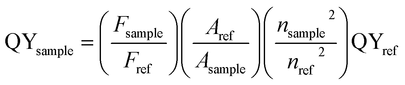
The calculated band structure of Zn1−xSnxO is shown in Fig. 2. It suggests that Zn1−xSnxO changed from direct gap semiconductors to indirect gap semiconductors with the Sn2+ content increasing to x = 0.0278. The Egap of Zn1−xSnxO first decreased from 0.806 eV to 0.197 eV when the Sn2+ content increased from 0 to 0.0625 and then it increased to 0.722 eV with increasing Sn2+ content.
 | ||
| Fig. 2 Calculated band structure and summarized Egap of Zn1−xSnxO. | ||
As reported, the band gap of ZnO should be 3.37 eV. However, our calculated results showed that the band gap of ZnO was 0.806 eV, which is much less than the reported band gap. The reason for this was that there are some deficiencies of the DFT/GGA during the calculations of transition metal oxides, particularly for ZnO.20–22 Usually, the LDA+U method was employed to solve this problem. However, the LDA+U method does not lead to the correction of the band gap.22,23 The main idea for this study was to discuss the effect of Sn content on the band structure of Sn-doped ZnO. As a result, only the changing trend in the band structure was required, the exact band structure, especially the exact band gap was not required. In other words, LDA+U was not required in this study.4,7
Fig. S1† shows the calculated total DOS (DOS) and partial DOS (PDOS) of Zn1−xSnxO. As shown in this figure, the valence band maximum was mainly derived from the O 2p orbital, and the conduction band minimum was mainly derived from Sn 5s and Sn 5p states.23 It appeared that with more Sn2+ doping, the shape, location and energy of these PDOS peaks changed. Sn 5p states became stronger, whereas O 2p orbital became weaker.
Fig. 3 shows the HRTEM and EDX figures of Sn2+ doped Zn0.95Sn0.05O and Zn0.91Sn0.09O QDs synthesized at 40 °C with 180 W of ultrasonic power for 30 min. It was observed that Sn2+ doped ZnO QDs have a uniform size around 2.6 nm, which was similar to the ZnO QDs synthesized under the same conditions.14 It also means that size effects on the band gap of Sn2+-doped ZnO QDs could be ignored.
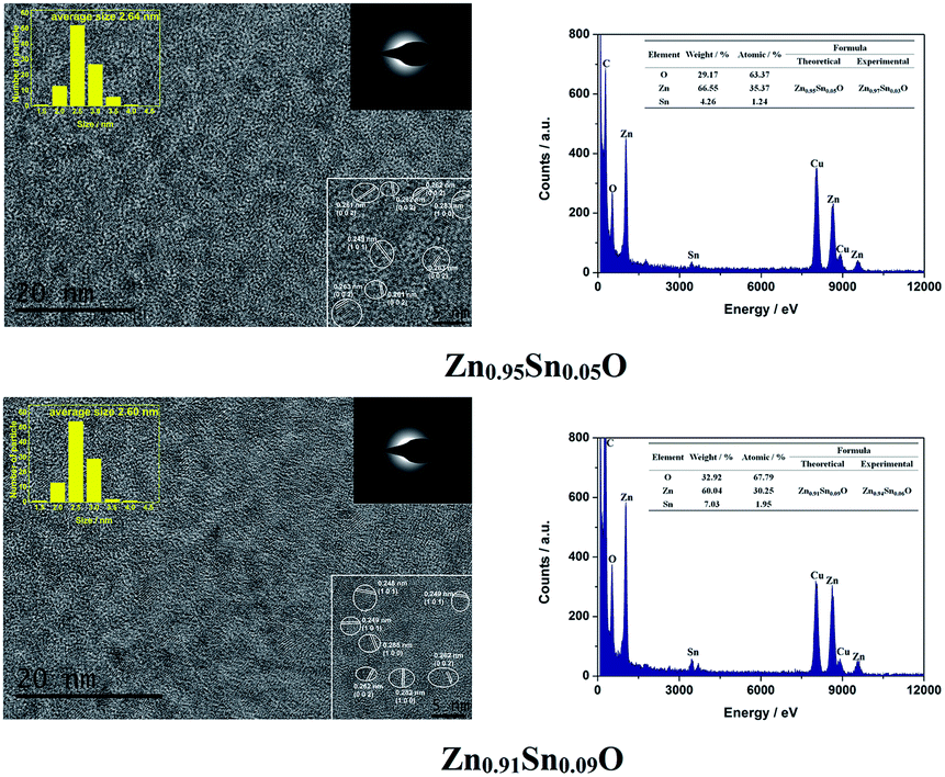 | ||
| Fig. 3 HRTEM and EDX of Sn2+ doped Zn0.95Sn0.05O and Zn0.91Sn0.09O QDs synthesized at 40 °C with 180 W of ultrasonic power for 30 min. | ||
Moreover, it was difficult to find the SnO2 (0.335) or SnO (0.299) phase24–26 in the HRTEM figure. It appeared that Sn2+-doped ZnO QDs still maintained the main phase of ZnO, which was different from those of the Sn-doped ZnO NPs with a high Sn concentration24–26 but was the same as that of the Sb doped ZnO with a low Sb concentration.27 The interplanar spacing increased with increasing Sn2+ concentration. This was similar to the trend in the calculated cell parameters of Zn1−xSnxO, as shown in Table 1.
Both Zn and Sn appeared in the EDX spectra. The atomic percentage of Zn, Sn and O are given in the figure as well. The possible formulas of these samples were Zn0.97Sn0.03O and Zn0.94Sn0.06O, which approached to the theoretical formulas Zn0.95Sn0.05O and Zn0.91Sn0.09O. Therefore, Sn was successfully doped into the lattice of ZnO.
Fig. 4 shows the XPS spectra of Zn1−xSnxO QDs synthesized at 40 °C with 180 W of ultrasonic power for 30 min. All the data were corrected with respect to the standard peak of C 1s at 284.6 eV.27–30 As shown in Fig. 4, for all the samples, both Sn and Zn peaks could be found in the XPS spectra. This was the same as the results from the EDX spectra. All the peaks of O, Zn and Sn were narrow and symmetric with FWHMs about 3 eV.
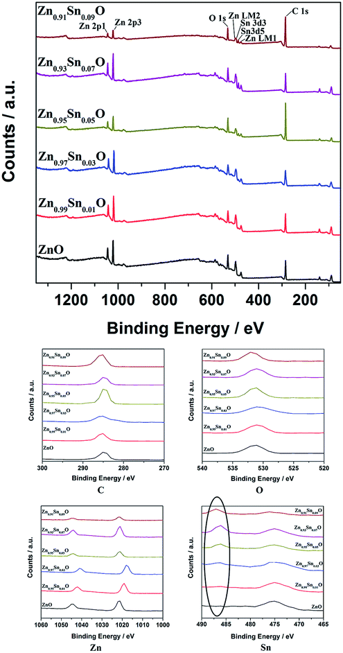 | ||
| Fig. 4 XPS spectra of Zn1−xSnxO QDs synthesized at 40 °C with 180 W of ultrasonic power for 30 min. | ||
For Zn 2p1 and Zn 2p3 at the same x values, the binding energy first decreased when x increased to 3 and then returned to the ZnO level.
The binding energy of O 1s peaks centered at 530.15 eV (O I) belongs to the O2− ions in the wurtzite structure of ZnO. Peaks centered at 531.25 eV (O II) belong to the oxygen vacancy defects, and peaks centered at 532.40 eV (O III) belong to the loosely bound oxygen on the surface of ZnO.30 Fitted spectra of O 1s peaks of Sn2+-doped ZnO are shown in Fig. S2.† It shows that, when the x value was less than 3, the main charge state of oxygen was the O2− ions in the wurtzite structure of ZnO. Then, the main oxygen state changed to oxygen vacancy defects and finally, to loosely bound oxygen.
The reason for the decrease in binding energy when x was less than 3 could be that when the concentration of Sn2+ was low, the way of Sn doping was interstitial. For a high Sn2+ concentration, the way of Sn doping changed to substitution. When x was larger than 5, with more Sn2+ doping, the concentration of  defects decreased, whereas the concentration of OZn and Oi defects increased.
The intensity of Sn 3d5 and Sn 3d3 increased with increasing x values. This means that the real Sn concentration in Sn doped ZnO QDs increased with more Sn2+ doping. The atomic percentages of Zn and Sn for all the samples are shown in Table 2. It appears that, with increases in the Sn2+ concentration in the raw material, the Sn concentration in Zn1−xSnxO QDs increased. Even the value of the Sn content obtained from XPS was much larger than the theoretical Sn concentration. The changing trend in the Sn concentration still was close to what we expected.
| x value | Zn/at% | Sn/at% | Formula |
|---|---|---|---|
| 0 | 100 | 0 | ZnO |
| 1 | 99.5 | 0.5 | Zn0.995Sn0.005O |
| 3 | 98 | 2 | Zn0.98Sn0.02O |
| 5 | 93 | 7 | Zn0.93Sn0.07O |
| 7 | 88 | 12 | Zn0.88Sn0.12O |
| 9 | 83 | 17 | Zn0.83Sn0.17O |
Fig. 5(a) shows the UV-Vis absorption spectra of Zn1−xSnxO QDs synthesized at 40 °C with 180 W of ultrasonic power for 30 min. All sample absorptions started from about 350 nm. As the Sn2+ content increased, the 99% absorption wavelength first increased from 350.5 nm to 370.5 nm until x = 0.03 and then decreased to 343 nm.
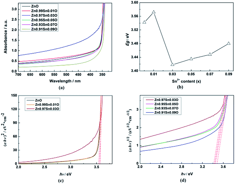 | ||
| Fig. 5 (a) UV-Vis absorption spectra, (b) calculated Egap, (c) the plot of (αhν)2 vs. (hν), (d) the plot of (αhν)1/2 vs. (hν) of Zn1−xSnxO QDs synthesized at 40 °C with 180 W of ultrasonic power for 30 min. | ||
ZnO is a direct gap semiconductor,31,32 which can be seen in Fig. 2. Formula (2) could change to Formula (3). This also means that (αhν)2 is proportional to (hν − Egap), and Egap is the intercept on the x-axis.
| (αhν)2 = A2(hν − Egap) | (3) |
As shown in Fig. 5, the calculated Egap for ZnO QDs is 3.542 eV, which is similar to the reported band gap of ZnO.
After Sn2+ doping, Zn1−xSnxO QDs changed to an indirect gap semiconductor, as shown in Fig. 2. Formula (2) could also change to Formula (4), which means that (αhν)1/2 is proportional to (hν − Egap), and Egap is the intercept on the x-axis.
| (αhν)1/2 = A(hν − Egap) | (4) |
The calculated Egap for all samples is given in Fig. 5(b–d). As shown in Fig. 5(b), with increasing Sn2+ content, the Egap of Zn1−xSnxO QDs first increased from 3.542 eV to 3.572 eV, dropped to 3.418 eV, and finally increased to 3.480 eV. Egap increased to the minimum point when the Sn2+ content reached 0.03. All of these are larger than the band gap of a ZnO single-crystal (3.37 eV).31,32 This was due to the energy band of QDs being quasi-continuous owing to their small size.31
The calculated Egap of Zn1−xSnxO first decreased then increased, and the inflection point of Sn2+ content (x) is 0.03, which is shown in Fig. 2. It seem that, changing trends in the calculated and experimental Egap of Zn1−xSnxO are almost the same.
Photoluminescence properties could reflect the band structures, sizes and defects of Zn1−xSnxO QDs. Fig. 6 shows the photoluminescence properties of Zn1−xSnxO QDs synthesized at 40 °C with 180 W of ultrasonic power for 30 min.
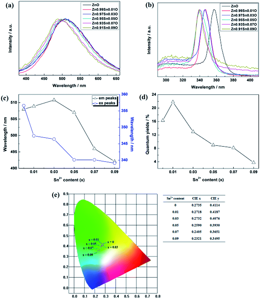 | ||
| Fig. 6 Photoluminescence properties of Zn1−xSnxO QDs synthesized at 40 °C with 180 W of ultrasonic power for 30 min. (a) emission spectra (b) excitation spectra (c) emission and excitation peaks (d) quantum yield (e) CIE diagram. | ||
As reported, the energy bands of quantum dots are determined by the size and band structures of Zn1−xSnxO QDs. Under same quantum dot concentration,15,18 the change in Zn1−xSnxO QDs excitation peaks was connected to the change in Zn1−xSnxO QDs band structures and sizes.13 For the ZnO quantum dots synthesized under the same condition, the size could be almost the same, meaning the excitation peaks could reflect the band structures of Zn1−xSnxO QDs.
Fig. 6(b) shows the excitation spectrum of the Zn1−xSnxO QDs. As shown in Fig. 6(b) and (c), with increasing Sn2+ content, the excitation peaks of Zn1−xSnxO QDs first decreased from 357 nm to 339 nm and then remained unchanged. The excitation peak of Zn1−xSnxO QDs is related to the energy band of ZnO base.5,33 This means that as the Sn2+ content increased, the energy band of the ZnO base increased.
Compared to the changing trend of Egap obtained by the absorption spectrum in Fig. 5, the trend is different. The Egap, calculated from the absorption spectrum, first decreased, then increased with more Sn2+ doping, and then approached the calculated results. However, the band gap inferred from the excitation peaks increased along with the Sn2+ content increasing. Due to the Moss–Burstein effect,34 when doping Sn atoms into the bulk, the band gap of ZnO grew wider, resulting in a blue shift of the excitation peaks.
To verify this, Dmol3 was employed to calculate the orbital properties of Sn2+-doped ZnO.35,36 As shown in Fig. S3,† with an increasing Sn2+ content, the conduct band minimum (CBM) first decreased and then increased, while the valence band maximum (VBM) decreased. Moreover, Ev − Ec increased with Sn2+ doping. This result approached the changing trend in the excitation peaks.
Fig. 6(a) and (e) show the emission spectra of Zn1−xSnxO QDs. Spectral shapes of Zn1−xSnxO QDs synthesized with different Sn2+ content were almost the same. The emission peaks were between 490 nm to 510 nm. With the addition of Sn2+, the emission peaks and blue emission shifted from yellow-green to blue-green.
The trend in emission and excitation peaks reflected the transformation between optical defects inside Zn1−xSnxO QDs. As reported, the green photoluminescence near 500 nm of ZnO bulk (with the optical gap of 3.37 eV) is mainly brought about by (1) a transition from near the conduction band edge to a deep acceptor level by OZn (2.38 eV) or Oi (2.24 eV), and (2) the transition from a deep donor level by  to a valence band (2.43 eV).5,11,37–39 This implies that, for the ZnO QDs with OZn or Oi defects, the changing trend in emission peaks should be the same as that of the excitation peaks. While for ZnO QDs with
  defects, the emission peaks might stay at about 510 nm, regardless of the change in size of the ZnO QDs.
Fig. 6(c) shows that with increasing Sn2+ content, the emission peaks first increased from 508 nm to 511 nm, and then dropped to about 492 nm again. It means that, under low Sn2+ content, main optical defects of Zn1−xSnxO QDs were  defects. With increasing Sn2+ content, some
  defects changed to OZn and Oi defects. This is due to the fact that the Sn2+ was not stable and could easily change to Sn4+. This process introduced O into Zn1−xSnxO QDs, which eliminated the
  defects and created OZn and Oi defects.
Fig. 6(d) shows the trend in Zn1−xSnxO QDs quantum yields influenced by Sn2+ content. The quantum yields of Zn1−xSnxO QDs first increased from 16.3% to 21.8% with little Sn2+ doping when x = 0.01. Then, the quantum yield sharply decreased to 3.7% with more Sn2+ doping.
It was reported that quantum yields of ZnO QDs are related to their optical defects. Introducing more optical defects15 could improve the quantum yields of ZnO QDs. However, quantum yields of QDs were also determined by the electronic traps,40 particularly the dangling bond defects on the surface of ZnO QDs. This means that passivation of the surface-state traps would improve the quantum yields of QDs as well.41 With an increase in Sn2+ content, the OH− dangling bonds on the surface of Zn1−xSnxO QDs decreased due to the Sn2+–Sn4+ transformation. This is advantageous to increase the quantum yield. However, with more Sn2+ doping, the Sn2+–Sn4+ transformation caused the concentration of  defects to decrease. This was the reason for the decrement of quantum yields of Zn1−xSnxO QDs when there were more Sn2+ ions. Moreover, it was reported that an indirect gap semiconductor has a poorer photoluminescence than that for the direct gap semiconductor.42 As mentioned, with Sn2+ content (x) increased to 0.03, the Zn1−xSnxO QDs changed from direct gap semiconductors to indirect gap semiconductors. As a result, the quantum yields slightly increased at first and then sharply dropped.
Sn4+ doped ZnO
The calculated cell parameters of Zn1−ySnyO are shown in Table 3.| Sn4+ content | a | b | c | α | β | γ | V | Sn–O | Zn–O |
|---|---|---|---|---|---|---|---|---|---|
| 0% | 0.3249 nm | 0.3249 nm | 0.5205 nm | 90.0° | 90.0° | 120.0° | 0.04759 nm3 | — | 0.1982 nm |
| 1.39% | 0.3249 nm | 0.3249 nm | 0.5205 nm | 90.0° | 90.0° | 120.0° | 0.04759 nm3 | 0.2058 nm | 0.1981 nm |
| 1.85% | 0.3273 nm | 0.3273 nm | 0.5238 nm | 90.0° | 90.0° | 120.1° | 0.04855 nm3 | 0.2112 nm | 0.1997 nm |
| 2.78% | 0.3322 nm | 0.3321 nm | 0.5385 nm | 90.0° | 90.0° | 120.7° | 0.05103 nm3 | 0.2084 nm | 0.2026 nm |
| 4.17% | 0.3331 nm | 0.3338 nm | 0.5363 nm | 90.0° | 90.0° | 121.0° | 0.05113 nm3 | 0.2176 nm | 0.2025 nm |
| 6.25% | 0.3349 nm | 0.3348 nm | 0.5382 nm | 90.2° | 89.9° | 121.0° | 0.05173 nm3 | 0.2202 nm | 0.2026 nm |
| 12.5% | 0.3377 nm | 0.3376 nm | 0.5341 nm | 90.4° | 89.6° | 121.2° | 0.05206 nm3 | 0.2242 nm | 0.2018 nm |
As shown in Table 3, with an increase in the Sn4+ content, the cell parameters changed. Similar to that of Zn1−xSnxO, the symmetry of Zn1−ySnyO was reduced by Sn4+ doping. With more Sn4+ doping, the space group of Zn1−ySnyO first changed from hexagonal to monoclinic and then changed to triclinic. The cell volume of Zn1−ySnyO increased from 0.04759 nm3 to 0.05206 nm3 when y increased. The length of the Sn–O bond increased from 0.2058 nm to 0.2242 nm. Even the sizes of Sn4+ ionic radii (0.069 nm) were smaller than that of the Zn2+ ion (0.074 nm). The charge of Sn4+ is larger than that of Zn2+, which means that the repulsion between Sn4+ and Zn2+ is larger than that between Zn2+ and Zn2+ as well as that between Sn2+ and Zn2+. That is why Sn4+ doping could also stretch the ZnO cells. However, for the Zn–O bond, the change in bond length was just from 0.1982 nm to 0.2026 nm, and then it decreased to 0.2018 nm, which was not significant. The increment was because of the cell enlarging, and the decrement was because of the Sn–O bond stretching.
The calculated band structure of Zn1−ySnyO is shown in Fig. 7. It suggests that Zn1−ySnyO changed from a direct gap semiconductor to an indirect gap semiconductor with an increase in the Sn4+ content to y = 0.0185, which is similar to that of Sn2+ doping ZnO. The Egap of Zn1−ySnyO first decreased from 0.806 eV to 0.224 eV when the Sn4+ content rose from 0 to 0.0278 and then it increased to 0.701 eV with a rise in the Sn4+ content.
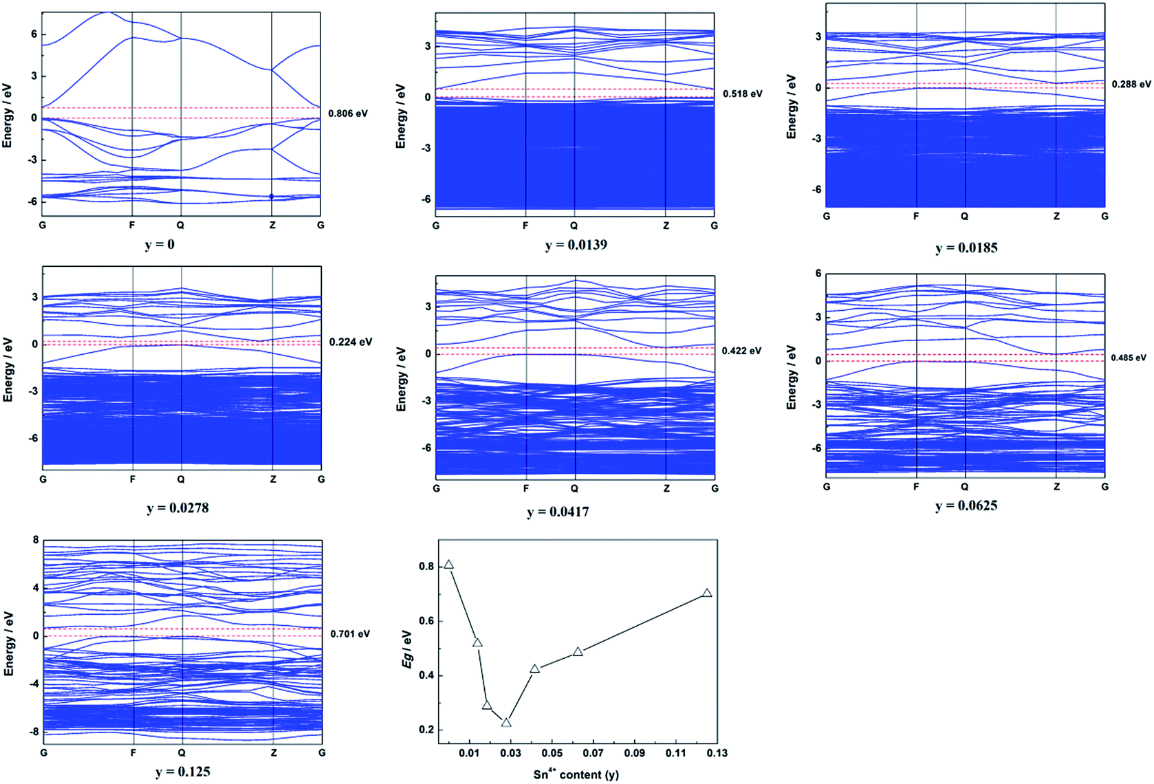 | ||
| Fig. 7 Calculated band structure and summarized Egap of Zn1−ySnyO. | ||
Compared to the calculated Egap of Sn2+-doped ZnO (Zn1−xSnxO), there are some differences. First, the inflection point of the Egap is different. For Zn1−xSnxO, the inflection point is about x = 0.0625, whereas for Zn1−ySnyO, y = 0.0278. Second, the value of Egap for the inflection point is different. For Zn1−ySnyO, it is 0.224 eV, whereas for Zn1−xSnxO, it is 0.197 eV, which is smaller than that of Zn1−ySnyO.
Fig. S4† displays the calculated total DOS (DOS) and partial DOS (PDOS) of Zn1−ySnyO. The changing trend in total DOS (DOS) and partial DOS (PDOS) of Zn1−ySnyO is similar to those of Zn1−xSnxO. As shown in the figure, the valence band maximum is also derived mainly from the O 2p orbital, and the conduction band minimum is derived mainly from Sn 5s and Sn 5p states.23 It appears that, with more Sn4+ doping, the shape, location and energy of these PDOS peaks changed. Sn 5p states became stronger, whereas the O 2p orbital became weaker. Moreover, compared with the Sn2+-doped ZnO samples, the shape, location and energy of Sn 5p states were quite different. That might be the reason why the trend in the band gap was different.
Fig. 8 shows the HRTEM and EDX figures of Sn4+ doped Zn0.95Sn0.05O and Zn0.91Sn0.09O QDs synthesized at 40 °C with 180 W of ultrasonic power for 30 min. Moreover, Sn4+ doped ZnO QDs have a uniform size around 2.6 nm, which is similar to that of the ZnO QDs14 and Sn2+-doped ZnO QDs synthesized under the same conditions. Sizes effects on the band gap of Sn4+ doped ZnO QDs could also be ignored.
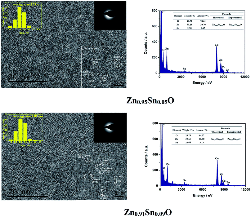 | ||
| Fig. 8 HRTEM and EDX of Sn4+ doped Zn0.95Sn0.05O and Zn0.91Sn0.09O QDs synthesized at 40 °C with 180 W of ultrasonic power for 30 min. | ||
It is difficult to find a SnO2 (0.335) or SnO (0.299) phase24–26 in the figure as well. It appears that Sn4+ doped ZnO QDs also could maintain the main phase of ZnO, which is similar to Sn2+ doped ZnO with a low Sn concentration. The interplanar spacing increased with increasing Sn4+ concentration. Interplanar spacings of Zn1−ySnyO were larger than those of Zn1−xSnxO at the same Sn concentration. This approached the calculated results of Zn1−ySnyO shown in Table 3.
Both Zn and Sn could be found in the EDX spectra as well. The atomic percentages of Zn, Sn and O are given in the figure as well. The possible formulas of these samples were Zn0.97Sn0.03O and Zn0.91Sn0.09O, which also approached the theoretical formulas Zn0.95Sn0.05O and Zn0.91Sn0.09O. Therefore, Sn4+ was successfully doped into the lattice of ZnO just like Sn2+ ions.
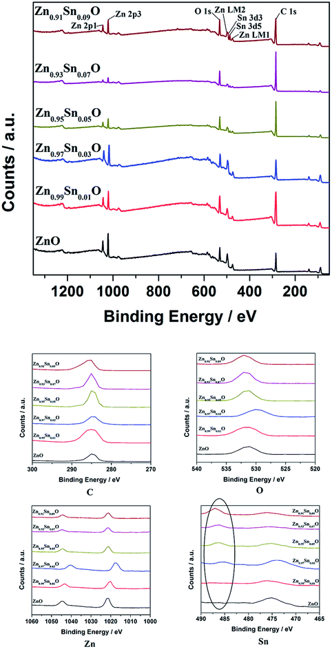
Fig. 9 shows the XPS spectra of Zn1−ySnyO QDs synthesized at 40 °C with 180 W of ultrasonic power for 30 min. All the data were corrected with respect to the standard peak of C 1s at 284.6 eV. As shown in Fig. 9, for all the samples, both Sn and Zn peaks are observed in the XPS spectra. The peaks of O, Zn and Sn were narrow and symmetrical with FWHM about 3 eV. This is same as the results of EDX shown in Fig. 8.
 | ||
| Fig. 9 XPS spectra of Zn1−ySnyO QDs synthesized at 40 °C with 180 W of ultrasonic power for 30 min. | ||
In the same way as Sn2+-doped ZnO QDs, the binding energy of Zn 2p1 and Zn 2p3 peaks first decreased when y increased to 3 and then returned to the ZnO level.
It appears that the changing trend in the type of oxygen was almost the same as that of the Sn2+ doped ZnO QDs. When the y value was less than 3, the main type of oxygen was the O2− ions in the wurtzite structure of ZnO. This could be due to the same reason as that in Sn2+ doped ZnO QDs, mentioned earlier.
However, there are fewer  defects in Sn4+-doped ZnO QDs than in Sn2+-doped ZnO QDs. The reason for this is that, in Sn4+-doped ZnO QDs, Sn4+ has a larger charge than Zn2+, and
  defects could not exist stably.
The reason could also be that when the concentration of Sn4+ is low, the way of Sn doping is interstitial. However, for high Sn4+ concentration, the way of Sn doping changed to substitution, which is similar to that of Sn2+-doped ZnO QDs.
The intensity of Sn 3d5 and Sn 3d3 increased with increasing y values as well. This suggests that the Sn concentration in Sn-doped ZnO QDs increased with more Sn4+ doping. The atomic percentage of Zn and Sn for all of the samples is shown in Table 4. It appears that with an increasing Sn4+ concentration in the raw material, the Sn concentration in Zn1−ySnyO QDs increased. The changing trend in the Sn concentration still approached the expected trend.
| x value | Zn/at% | Sn/at% | Formula |
|---|---|---|---|
| 0 | 100 | 0 | ZnO |
| 1 | 99.6 | 0.4 | Zn0.996Sn0.004O |
| 3 | 94 | 6 | Zn0.94Sn0.06O |
| 5 | 91 | 9 | Zn0.91Sn0.09O |
| 7 | 86 | 14 | Zn0.86Sn0.14O |
| 9 | 81 | 19 | Zn0.81Sn0.19O |
Fig. 10(a) displays the UV-Vis absorption spectra of Zn1−ySnyO QDs synthesized at 40 °C with 180 W of ultrasonic power for 30 min. All sample absorptions started from about 350 nm. With an increasing Sn4+ content, the 99% absorption wavelength decreased from 350.5 nm to 341 nm when y = 0.03 and then remained at the same level.
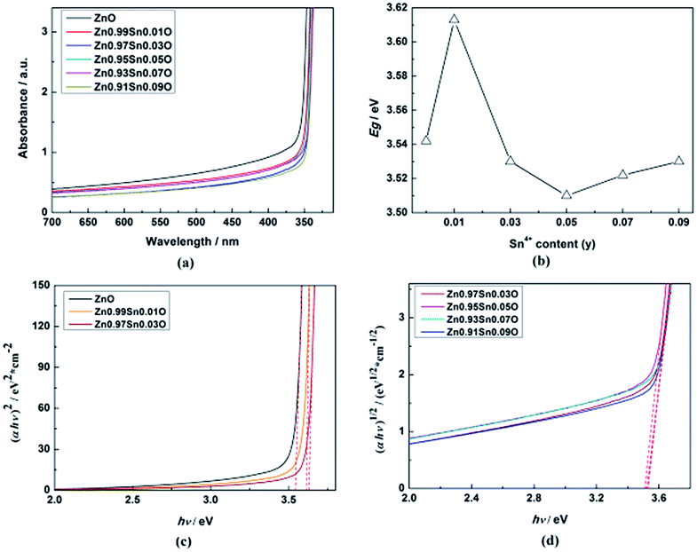 | ||
| Fig. 10 (a) UV-Vis absorption spectra, (b) calculated Egap, (c) the plot of (αhν)2 vs. (hν), (d) the plot of (αhν)1/2 vs. (hν) of Zn1−ySnyO QDs synthesized at 40 °C with 180 W of ultrasonic power for 30 min. | ||
As shown in Fig. 7, when the content of Sn4+ was raised to y = 0.0278, Zn1−ySnyO changed from a direct gap semiconductor to an indirect gap semiconductor. Formula (3) and (4) could also be used to calculate the Egap of Zn1−ySnyO QDs.
The calculated Egap for all samples is given in Fig. 10(b–d). As shown in Fig. 10(b), with increasing Sn4+ content, the Egap of Zn1−ySnyO QDs first increased from 3.542 eV to 3.613 eV and then dropped to 3.510 eV, but finally rose to 3.530 eV. The Egap reached the minimum point when the Sn4+ content reached 0.05.
The calculated Egap of Zn1−ySnyO first decreased and then increased, and the inflection point of Sn4+ content (y) was 0.0278 (Fig. 7). The changing trend in the calculated Egap of Zn1−ySnyO was identical to that of the experimental Egap.
Compared to Sn2+-doped samples, the Egap of all Zn1−ySnyO samples was larger than those of Zn1−xSnxO samples. This phenomenon corresponds to the calculated results. It implies that the impurity levels of Sn4+ are higher than those of Sn2+.
Fig. 11 shows the photoluminescence properties of Zn1−ySnyO QDs synthesized at 40 °C with 180 W of ultrasonic power for 30 min.
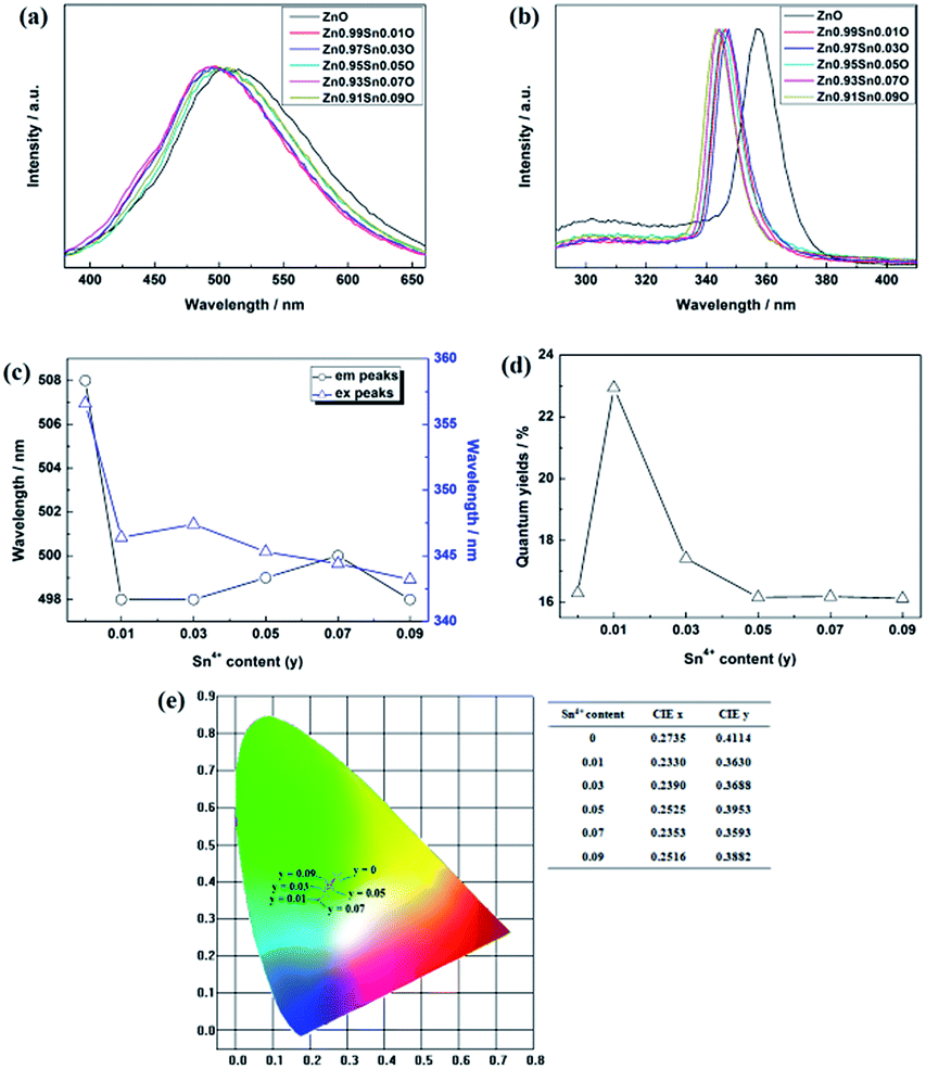 | ||
| Fig. 11 Photoluminescence properties of Zn1−ySnyO QDs synthesized at 40 °C with 180 W of ultrasonic power for 30 min. (a) emission spectra (b) excitation spectra (c) emission and excitation peaks (d) quantum yield (e) CIE diagram. | ||
Fig. 11(b) shows the excitation spectrum of the Zn1−ySnyO QDs. The excitation peak of Sn-doped ZnO QDs is related to the energy band of the ZnO base. From Fig. 11(b) and (c), it is clearly seen that with increasing Sn4+ content, the excitation peaks of Zn1−ySnyO QDs decreased from 357 nm to 343 nm. This suggests that the energy band of the ZnO base increased with an increasing Sn4+ content as well.
Compared to the results obtained by the absorption spectrum in Fig. 10, the changing trend is different. For the Egap calculated from the absorption spectrum, it first decreased and then increased with Sn4+ doping. However, the Egap inferred from the excitation peaks increased along with an increasing Sn4+ content. This trend is the same as that of the Sn2+-doped samples for the same reason mentioned in Section 3.1. Furthermore, the excitation peaks of Zn1−ySnyO QDs were larger than those of Zn1−xSnxO QDs for same Sn content. This means that the band gaps of Sn2+-doped ZnO bases were larger than those of Sn4+-doped ZnO bases. However, the opposite of this was observed for the Egap of Zn1−ySnyO QDs and Zn1−xSnxO QDs. This means that Sn2+ could enlarge the band gap of the ZnO base more effectively than Sn4+, while the energy levels of Sn4+ were higher than those of Sn2+.
To verify this, Dmol3 was also employed to calculate the orbital properties of Sn4+-doped ZnO.35,36 As shown in Fig. S6,† with an increasing Sn4+ content, the CBM first decreased and then increased, while the VBM decreased, and Ev − Ec increased with Sn4+ doping. Compared to Sn2+ doped ZnO, the changing trends in both CBM, VBM and Ev − Ec are almost the same. Furthermore, Ev − Ec of Sn2+-doped ZnO was larger than that of Sn4+-doped ZnO. Moreover, these results approached the results obtained by the excitation peaks.
Fig. 11(a) and (e) show the emission spectra of Zn1−ySnyO QDs. The spectral shapes of Zn1−ySnyO QDs synthesized with different Sn4+ content are almost the same. The emission peaks were between 490 nm to 510 nm. With the addition of Sn4+, the emission peaks and emitting color first blue-shifted from yellow-green to blue-green and then redshifted to green again.
Fig. 11(c) shows that with an increasing Sn4+ content, the emission peaks decreased from 508 nm to 498 nm and then remained at the same level. This implies that for Sn4+-doped ZnO QDs, the main optical defects were Oi and OZn defects. The reason for this is that the valence of Sn4+ is 4, which is larger than Zn2+ and Sn2+. To maintain the conservation of electricity,  defects could not exist stably in the Zn1−ySnyO crystal, while Oi and OZn defects could exist.
Fig. 11(d) shows the changing trend of Zn1−ySnyO QDs quantum yields influenced by the Sn4+ content. The quantum yields of Zn1−xSnxO QDs first increased from 16.3% to 22.9% with a slight amount of Sn4+ doping when y = 0.01. Then, the quantum yield decreased to 16.2% when the Sn4+ content increased to 0.05, and finally remained at the same level. There is no doubt that quantum yields of Zn1−ySnyO QDs were larger than those of Zn1−xSnxO QDs. With an increased Sn4+ content, the concentration of Oi and OZn defects increased. Moreover, OH− dangling bonds on the surface of Zn1−ySnyO QDs decreased due to the formation of Oi and OZn defects as well. These are advantageous to increase the quantum yield.
For the negative part of quantum yield, after the Sn4+ content (y) increased to 0.03, Zn1−ySnyO QDs changed from a direct gap semiconductor to an indirect gap semiconductor. As mentioned, the indirect gap could reduce the luminescence. As a result, the quantum yields decreased when the Sn4+ content reached 0.03. However, more Sn4+ doping means more Oi and OZn optical defects and less OH− dangling bonds on the surface. The positive part and negative part of Zn1−ySnyO QDs quantum yields could counteract. This is why the quantum yields of Zn1−ySnyO QDs remained at the same level when the Sn4+ content was larger than 0.05.
Compared to that of Zn1−xSnxO QDs, the changing trend of optical defects concentration in Zn1−ySnyO QDs is different. As mentioned in Section 3.1 for the Zn1−xSnxO QDs, with an increasing Sn2+ content, the concentration of their optical defects  decreased because of the creation of Oi and OZn defects. However, the main optical defects in Zn1−ySnyO QDs were Oi and OZn defects. With an increasing Sn4+ content, the concentration of optical defects increased. This is a possible reason why the quantum yields of Zn1−ySnyO QDs were larger than those of Zn1−xSnxO QDs.
Conclusions
In conclusion, the structure and band structure of Sn-doped ZnO QDs were investigated via DFT calculations and optical properties. It appears that both Sn2+ and Sn4+ doping could change ZnO from direct gap semiconductors to indirect gap semiconductors. With an increased Sn content, the band gap of Sn-doped ZnO first decreased and then increased. Sn2+ doping could reduce the band gap further. For the Sn-doped ZnO QDs synthesized by an ultrasonic method, the trends in the band gap were almost same as those obtained by DFT calculations. The band gap first decreased then increased with more Sn doping. Sn4+-doped ZnO QDs had a larger band gap than that of Sn2+-doped ZnO QDs.The changing trend in defects of Sn-doped ZnO was also interesting. The main optical defects of both Sn2+- and Sn4+-doped ZnO QDs changed from  defects (in ZnO QDs) to Oi and OZn defects. For Sn4+, this was due to its higher charge. However, for Sn2+, it was due to the change from Sn2+ to Sn4+. The changing trends in quantum yields of Sn2+-doped ZnO QDs and Sn4+-doped ZnO QDs were different. For Sn2+-doped ZnO QDs, not all of the Sn2+ transformed to Sn4+, while the
  defects still changed to Oi and OZn defects. As a result, the concentration of the main optical defects decreased. This made the quantum yields decrease with more Sn2+ doping. For Sn4+ doping, the main optical defects were Oi and OZn defects, with concentrations that were proportional to the content of Sn4+. As a result, the quantum yields increased with more Sn4+ doping.
Acknowledgements
The authors gratefully acknowledge the financial support of this study from the Project Funded by the Priority Academic Program Development of Jiangsu Higher Education Institutions (PAPD) and the National Natural Science Foundation of China (51202111).References
- M. S. Augustine, P. P. Jeeju, V. G. Sreevalsa and S. Jayalekshmi, J. Phys. Chem. Solids, 2012, 73, 396–401 CrossRef.
- Y. H. Tong, Y. C. Liu, S. X. Lu, L. Dong, S. J. Chen and Z. Y. Xiao, J. Sol-Gel Sci. Technol., 2004, 30, 157–161 CrossRef CAS.
- H.-J. Jeon, W. J. Maeng and J.-S. Park, Ceram. Int., 2014, 40, 8769–8774 CrossRef CAS.
- A. Mokhles Gerami and M. Vaez-Zadeh, J. Supercond. Novel Magn., 2016, 29, 1295–1302 CrossRef CAS.
- L.-W. Sun, H.-Q. Shi, W.-N. Li, H.-M. Xiao, S.-Y. Fu, X.-Z. Cao and Z.-X. Li, J. Mater. Chem., 2012, 22, 8221–8227 RSC.
- Z. Chen, D. Pan, Z. Li, Z. Jiao, M. Wu, C. Shek, C. Wu and J. Lai, Chem. Rev., 2014, 114, 7442–7486 CrossRef CAS PubMed.
- C. Supatutkul, S. Pramchu, A. P. Jaroenjittichai and Y. Laosiritaworn, Surf. Coat. Technol., 2016, 298, 53–57 CrossRef CAS.
- R. Sangeetha and S. Muthukumaran, Ceram. Int., 2016, 42, 5921–5931 CrossRef CAS.
- S. J. Clark, M. D. Segall, C. J. Pickard, P. J. Hasnip, M. I. J. Probert, K. Refson and M. C. Payne, Z. Kristallogr. - Cryst. Mater., 2005, 220, 567–570 CAS.
- J. P. Perdew, K. Burke and M. Ernzerhof, Phys. Rev. Lett., 1996, 77, 3865 CrossRef CAS PubMed.
- V. Kumar, H. C. Swart, M. Gohain, S. Som, B. C. Bezuindenhoudt and O. M. Ntwaeaborwa, Ultrason. Sonochem., 2014, 21, 1549–1556 CrossRef CAS PubMed.
- A. Khorsand Zak, W. H. Majid, H. Z. Wang, R. Yousefi, A. Moradi Golsheikh and Z. F. Ren, Ultrason. Sonochem., 2013, 20, 395–400 CrossRef CAS PubMed.
- W. Yang, L. Wang, X. Lu and Q. Zhang, J. Mater. Sci.: Mater. Electron., 2015, 26, 1113–1118 CrossRef CAS.
- W. Yang, B. Zhang, N. Ding, W. Ding, L. Wang, M. Yu and Q. Zhang, Ultrason. Sonochem., 2016, 30, 103–112 CrossRef CAS PubMed.
- W. Yang, H. Yang, W. Ding, B. Zhang, L. Zhang, L. Wang, M. Yu and Q. Zhang, Ultrason. Sonochem., 2016, 33, 106–117 CrossRef CAS PubMed.
- A. Schejn, M. Fregnaux, J. M. Commenge, L. Balan, L. Falk and R. Schneider, Nanotechnology, 2014, 25, 145606 CrossRef PubMed.
- H. R. Rajabi, M. Shamsipur, A. A. Khosravi, O. Khani and M. H. Yousefi, Spectrochim. Acta, Part A, 2013, 107, 256–262 CrossRef CAS PubMed.
- W. Yang, L. Wang, X. Lu, Y. Ding and Q. Zhang, Mater. Lett., 2015, 141, 330–332 CrossRef CAS.
- Y. Nakanishi, K. Kato, M. Horikawa and M. Yonekura, Thin Solid Films, 2016, 612, 231–236 CrossRef CAS.
- N. N. Lathiotakis, A. N. Andriotis and M. Menon, Phys. Rev. B: Condens. Matter Mater. Phys., 2008, 78, 193311 CrossRef.
- S. Massidda, R. Resta, M. Posternak and A. Baldereschi, Phys. Rev. B: Condens. Matter Mater. Phys., 1995, 52, R16977–R16980 CrossRef CAS.
- R. M. Sheetz, I. Ponomareva, E. Richter, A. N. Andriotis and M. Menon, Phys. Rev. B: Condens. Matter Mater. Phys., 2009, 80, 195314 CrossRef.
- B. Cao, T. Shi, S. Zheng, Y. H. Ikuhara, W. Zhou, D. Wood, M. Al-Jassim and Y. Yan, J. Phys. Chem. C, 2012, 116, 5009–5013 CAS.
- C. Chen, L. Wang, Y. Liu, Z. Chen, D. Pan, Z. Li, Z. Jiao, P. Hu, C. Shek, C. Wu, J. Lai and M. Wu, Langmuir, 2013, 29, 4111–4118 CrossRef CAS PubMed.
- J. Wang, Z. Chen, Y. Liu, C. Shek, C. Wu and J. Lai, Sol. Energy Mater. Sol. Cells, 2014, 128, 254–259 CrossRef CAS.
- L. Ren, D. Chen, Z. Hu, Z. Gao, Z. Luo, Z. Chen, Y. Jiang, B. Zhao, C. Wu and C. Shek, RSC Adv., 2016, 6, 82096 RSC.
- M. Gallegos, M. Peluso, H. Thomas, L. Damonte and J. Sambeth, J. Alloys Compd., 2016, 689, 416–424 CrossRef CAS.
- B. Song, C. Ji, Y. Zhu, Z. Geng, L. Zhang, Z. Lin, C. Tuan, K. Moon and C. Wong, Chem. Mater., 2016, 24, 9110–9121 CrossRef.
- B. Song, J. Zhao, M. Wang, J. Mullavey, Y. Zhu, Z. Geng and D. Chen, Nano Energy, 2017, 31, 183–193 CrossRef CAS.
- J. Lin, K. Peng, H. Liao and S. Lee, Thin Solid Films, 2008, 16, 5349–5354 CrossRef.
- J. R. Chelikowsky, Solid State Commun., 1977, 22, 351–354 CrossRef CAS.
- A. Kobayashi, O. F. Sankey and J. D. Dow, Phys. Rev. B: Condens. Matter Mater. Phys., 1983, 28, 946–956 CrossRef CAS.
- H. Zeng, S. Yang and W. Cai, J. Phys. Chem. C, 2011, 115, 5038–5043 CAS.
- H. Fujiwara and M. Kondo, Phys. Rev. B: Condens. Matter Mater. Phys., 2005, 71, 075109 CrossRef.
- B. Delley, J. Chem. Phys., 2000, 113, 7756–7764 CrossRef CAS.
- B. Delley, J. Chem. Phys., 1990, 92, 508–517 CrossRef CAS.
- K. Vanheusden, W. L. Warren, C. H. Seager, D. R. Tallant, J. A. Voigt and B. E. Gnade, J. Appl. Phys., 1996, 79, 7983–7990 CrossRef CAS.
- B. Lin, Z. Fu and Y. Jia, Appl. Phys. Lett., 2001, 79, 943 CrossRef CAS.
- H. S. Kang, J. S. Kang, J. W. Kim and S. Y. Lee, J. Appl. Phys., 2004, 95, 1246–1250 CrossRef CAS.
- J. J. Shi, S. Wang, T. T. He, E. S. Abdel-Halim and J. J. Zhu, Ultrason. Sonochem., 2014, 21, 493–498 CrossRef CAS PubMed.
- W. K. Bae, K. Char, H. Hur and S. Lee, Chem. Mater., 2008, 20, 531–539 CrossRef CAS.
- K. F. Mak, C. Lee, J. Hone, J. Shan and T. F. Heinz, Phys. Rev. Lett., 2010, 105, 136805 CrossRef PubMed.
Footnote |
| † Electronic supplementary information (ESI) available. See DOI: 10.1039/c6ra25940e |
| This journal is © The Royal Society of Chemistry 2017 |