DOI:
10.1039/C6RA25853K
(Paper)
RSC Adv., 2017,
7, 4724-4734
Reducing gas-sensing performance of Ce-doped SnO2 thin films through a cosputtering method†
Received
26th October 2016
, Accepted 3rd January 2017
First published on 17th January 2017
Abstract
SnO2 thin films doped with various concentrations of Ce were grown by cosputtering Sn and Ce metallic targets in an Ar/O2 mixed atmosphere. The cerium concentrations in the SnO2 films were varied from 1.2 to 4.5 at% by varying the Ce sputtering power during thin-film growth. Surface morphology analysis revealed that the surface roughness of the Ce-doped SnO2 thin films increased with an increase in cerium concentration. X-ray diffraction and transmission electron microscopy analysis results indicated that the Ce-doped SnO2 thin films were highly crystalline. Furthermore, Ce ions in the SnO2 thin films had mixed valence states; moreover, the oxygen vacancy density increased with an increase in Ce concentration. An increased Ce concentration in the SnO2 thin films engendered the roughening of the Ce-doped SnO2 film surface and increased the concentration of Ce4+ ions and oxygen vacancy number near the film surface. These factors are advantageous for enabling the adsorption of a relatively large number of oxygen ions on the film surface; therefore, increased ethanol vapor sensing responses of Ce-doped SnO2 thin films with an increase in Ce concentration were observed in this study.
Introduction
Tin dioxide (SnO2) is an n-type semiconductor with excellent optical and electrical properties. This semiconducting metal oxide is commercially used because of its numerous advantages, including low cost, high chemical stability, high sensitivity to various toxic gases, and compatibility with microfabrication processes.1–3 However, for application in gas-sensing devices, its gas-sensing performance requires further improvement for the specific detection of particular gases with high sensitivity. Several methods have been adopted for improving the efficiency of SnO2-based gas sensors. Morphological control has been widely used to fabricate SnO2 with a high specific surface area, thus enhancing its gas-sensing performance. Hierarchical SnO2 nanoflowers have exhibited visible acetic acid gas-sensing responses.4 SnO2 nanorods and nanowires exhibit visible H2 gas-sensing behavior.5,6 SnO2 sea-urchin nanostructures show visible hydrogen gas detection ability at room-temperature.7 Furthermore, the incorporation of some additives into SnO2 is another approach for improving the gas-sensing performance of SnO2 because doping can alter its structure and grain size or introduce surface defects. These factors are advantageous for enhancing the gas-sensing responses of SnO2 toward specific test gases. Ce-Doped SnO2 nanoparticles have been used as a sensing material for ammonia and a comparison has been made with its undoped form.8 Ce-Doped coral-like SnO2 nanostructures exhibit a promising candidate of highly sensitive and selective gas sensors for toluene.9 Pd and Ce codoped SnO2 thick films exhibit visible ethanol vapor detection ability;10 Ni and Ce codoped SnO2 thick films are of potential for sensing acetone vapor.11 Pr-Doped SnO2 hollow nanofibers exhibit an increased surface area, adsorbed oxygen species, and oxygen vacancy intensity; therefore, these nanofibers exhibit improved gas-sensing properties toward ethanol vapor.12 The formation of acceptor energy levels with the incorporation of Zn2+ ions into SnO2 improves the electrical conductivity of SnO2 nanospheres; therefore, Zn-doped SnO2 nanospheres exhibit a threefold increased response compared with undoped SnO2.13
Cerium as a dopant has received considerable attention because of its valuable properties arising from the availability of the 4f shell.14 This dopant has been incorporated into various metal oxides, for example, ZnO nanoparticles,15 In2O3 nanospheres,16 and SnO2 hollow nanofibers17 for improving their gas-sensing properties. Although SnO2 with various nanostructural morphologies exhibits a high specific surface area and is advantageous for improving gas-sensing performance, the incorporation of such low-dimensional nanomaterials into practical gas-sensing devices for obtaining high reliability remains a technological challenge. By contrast, the thin-film structure is a relatively well-established morphology for use in sensor materials with satisfactory device reliability and feasible commercial production. The doping of SnO2 thin films with Ce ions is thus valuable for understanding the correlation between the material design and gas-sensing performance of SnO2-based thin-film materials. Sputtering is the most widely used oxide thin-film growth process.18,19 It is compatible with the current processes used for manufacturing semiconductor devices. However, a limited number of reports on cosputtering growth of Ce-doped SnO2 thin films and the correlation between microstructures and gas-sensing properties are available. In this study, Ce-doped SnO2 composite thin films with varying concentrations of cerium were grown by cosputtering Sn and Ce metallic targets. The microstructural evolution and reducing gas-sensing properties of the as-grown Ce-doped SnO2 composite films with varying concentrations of cerium were investigated to study the effects of cerium doping on the material characteristics of the composite thin films.
Experiments
Undoped and Ce-doped SnO2 thin films were fabricated onto the 300 nm-thick SiO2/Si substrates using dual-gun sputtering system. Sn and Ce metallic discs with a size of 2 inches were used as sputtering targets to prepare Ce-doped SnO2 thin films. During growth of Ce-doped SnO2 thin films, the DC sputtering power of Sn target was fixed at 30 W; moreover, the RF sputtering power of Ce target varied from 20 to 60 W. The thin-film growth temperature was maintained at 300 °C with an Ar/O2 ratio of 25![[thin space (1/6-em)]](https://www.rsc.org/images/entities/char_2009.gif) :15; the gas pressure during sputtering thin-film deposition was fixed at 2.67 Pa.
:15; the gas pressure during sputtering thin-film deposition was fixed at 2.67 Pa.
The surface morphology of various thin films was investigated by scanning electron microscopy (SEM; Hitachi S-4800) and atomic force microscope (AFM; Veeco D5000). Sample crystal structures were investigated by X-ray diffraction (XRD; Bruker D2 PHASER) using Cu Kα radiation. X-ray photoelectron spectroscopy (XPS; PHI 5000 VersaProbe) analysis was used to determine the chemical binding status of constituent elements of undoped and Ce doped SnO2 films. The microstructures of the thin-film samples were characterized by high-resolution transmission electron microscopy (HRTEM; Philips Tecnai F20 G2). To measure reducing gas sensing properties, the silver paste was coated onto the surface of the undoped and Ce-doped SnO2 thin films to form electrodes for gas sensing measurements. The gas sensors made from undoped and Ce-doped SnO2 thin films were placed in a closed vacuum chamber, and various concentrations of ethanol vapor (50, 100, 250, 500, and 750 ppm) were introduced into the test chamber, using synthetic air as the carrier gas. The gas sensing response of the thin-film sensors to ethanol vapor is defined as the Ra/Rg. Ra is the sensor electrical resistance in the absence of target gas and Rg is that in the target gas.
Results and discussion
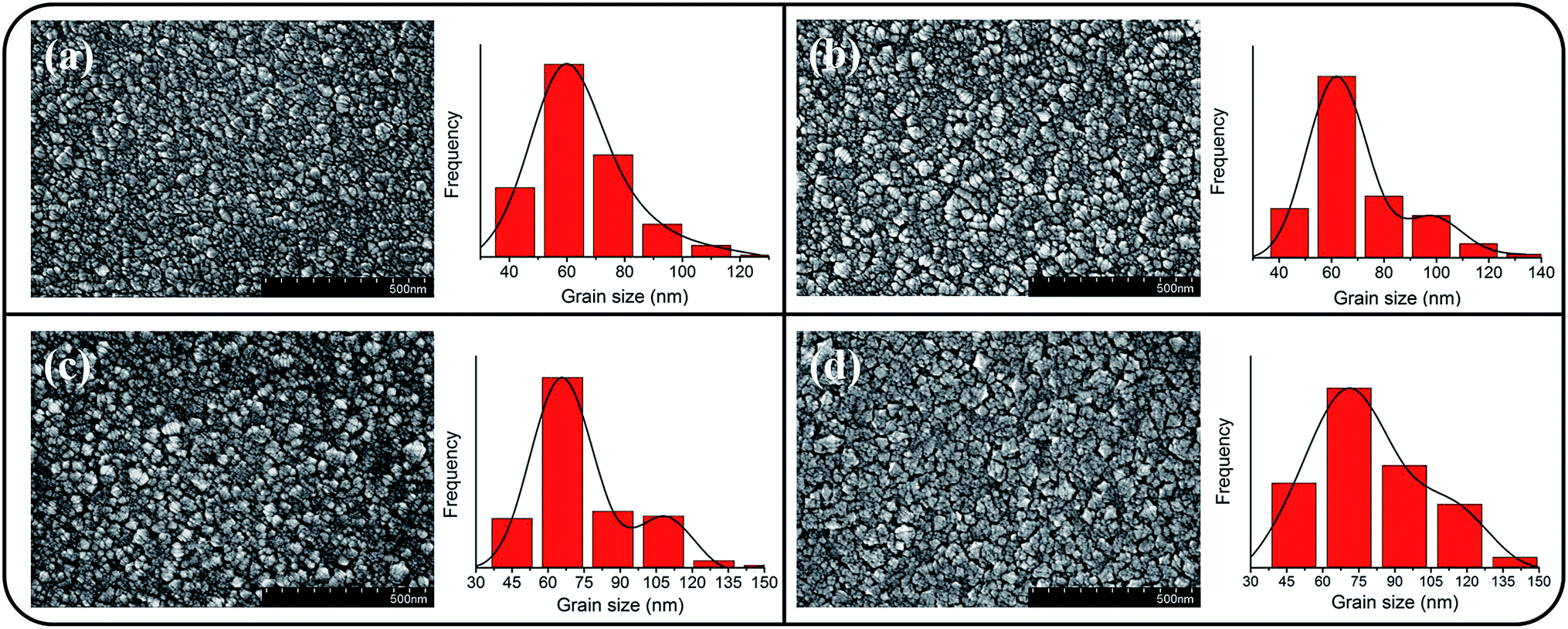
Fig. 1(a)–(d) depict the SEM micrographs of undoped and Ce-doped SnO2 thin films grown using various Ce sputtering powers. The surface of the pure SnO2 thin film consists of uniformly distributed grains measuring 10–35 nm (Fig. 1(a)). The film surface has tightly packed grains without any visible voids or cracks. Fig. 1(b)–(d) illustrate that the morphology of the surface grains of the SnO2 thin films with Ce doping is slightly coarser than that of the pure SnO2 thin film. Notably, grain boundaries among the surface grains of the SnO2 thin film became visible and broad with an increase in Ce sputtering power. The surface of the Ce-doped SnO2 thin films became rougher with an increase in Ce sputtering power. Fig. 2(a)–(d) depict the AFM images of the undoped and various Ce-doped SnO2 thin films. The root-mean-square surface roughness values are 4.53, 4.93, 5.14, and 6.31 nm for the undoped SnO2 thin film and Ce-doped films grown with Ce sputtering powers of 20, 40, and 60 W, respectively. The surface roughness evaluation results indicated that the surface roughness is correlated with the concentration of Ce in the SnO2 thin films; an increase in the concentration of Ce in the SnO2 deteriorates the smoothness of the film surface. In this study, an increase in the grain size engendered an increase in the surface roughness of the Ce-doped SnO2 thin films with an increase in Ce sputtering power. A similar surface roughening effect of doping was reported for other impurity-doped SnO2 thin films.20 A rougher surface feature of oxides is beneficial to increase interaction degree between the material surface and target gas molecules.21 The SEM and AFM observations indicated that SnO2 thin films doped with Ce at a higher sputtering power of 60 W might be promising for improving their gas-sensing performance.
 |
| | Fig. 1 SEM images of the Ce-doped SnO2 thin films prepared at various Ce sputtering powers: (a) 0 W, (b) 20 W, (c) 40 W, (d) 60 W. | |
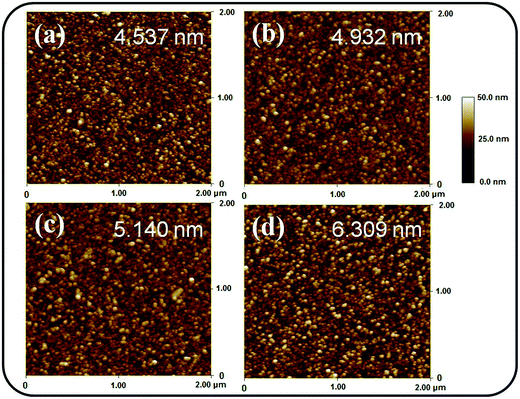 |
| | Fig. 2 AFM images of the Ce-doped SnO2 thin films prepared at various Ce sputtering powers: (a) 0 W, (b) 20 W, (c) 40 W, (d) 60 W. | |
The XRD patterns of undoped and Ce-doped SnO2 thin films prepared under various Ce sputtering powers are depicted in Fig. 3(a)–(d). The spectral lines exhibit diffraction peaks centered at approximately 26.6°, 33.8°, 37.9°, 51.7°, and 54.7°. All the Bragg reflections are ascribed to the tetragonal crystalline phase of tin oxide, and the Bragg reflections correspond to the SnO2 (110), (101), (200), (211), and (220) planes, respectively. No diffraction peaks of the CeO2 phase are visible in the XRD patterns (Fig. 3(b)–(d)), revealing that Ce might act as a substitutional ion on the Sn site in the SnO2 lattice. Similar XRD structural features were reported in Ce-doped SnO2 thin films prepared through a sol–gel synthesis method with a low Ce concentration range.22 In the current work, the undoped and Ce-doped SnO2 thin films were polycrystalline with a single SnO2 phase. The SnO2 (110) plane was the dominant crystallographic orientation in the SnO2 thin films grown with Ce sputtering powers of 20 and 40 W and without Ce doping. However, the high Ce sputtering power of 60 W caused SnO2 (200) to become the dominant crystallographic orientation of the SnO2 thin film. The peak intensity ratios of SnO2 (110) Bragg reflection to all crystallographic planes, I(110)/[I(110) + I(101) + I(200) + I(211) + I(220)], in the polycrystalline undoped and Ce-doped SnO2 thin films were calculated. The background intensity of the Bragg reflections was deducted before calculating the intensity ratio of Bragg peaks.23 The intensity ratio decreased from 0.53 to 0.22 when the Ce sputtering power was increased to 60 W. The crystallographic orientation feature of the Ce-doped SnO2 thin films changed with the Ce sputtering power. An appreciable difference in the ionic radius of Ce and Sn ions might engender lattice distortion of the SnO2 thin film with the addition of Ce dopants; this might be crucial in affecting the crystallographic plane growth feature during thin-film growth.24,25 A similar impurity dopant-dependent crystallographic feature change in matrix materials has been observed in other impurity-doped oxide films created using various synthesis methods.26,27
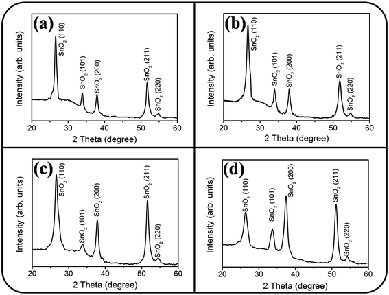 |
| | Fig. 3 XRD patterns of the Ce-doped SnO2 thin films prepared at various Ce sputtering powers: (a) 0 W, (b) 20 W, (c) 40 W, (d) 60 W. | |
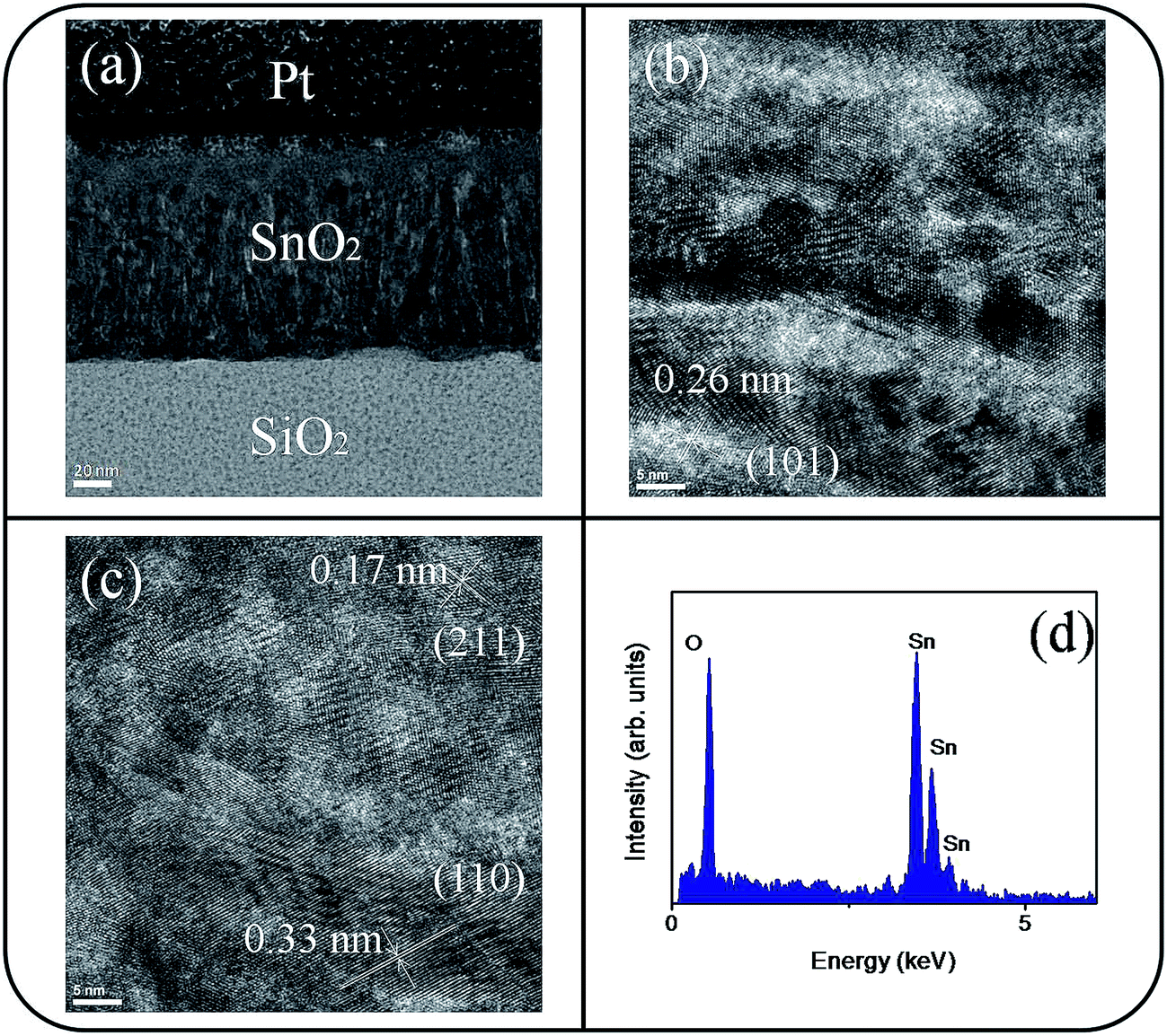
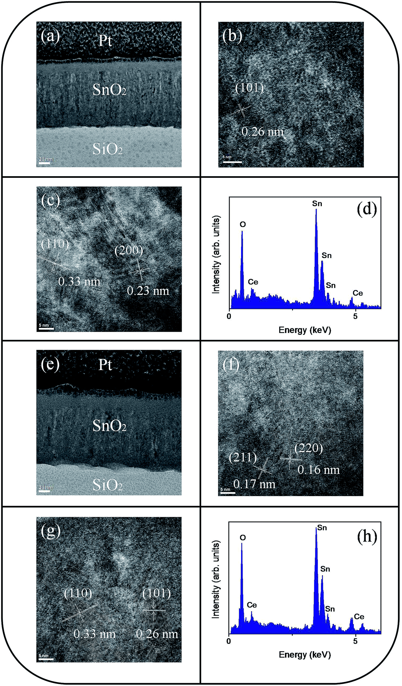
The microstructures of undoped and Ce-doped SnO2 thin films with Ce sputtering powers of 40 W and 60 W were further characterized through TEM. Fig. 4(a) shows a low-magnification, cross-sectional TEM image of the pure SnO2 thin film, which is composed of distinct columnar grains and has a thickness of approximately 120 nm. Various-sputtering deposited oxide thin films have been reported to exhibit a columnar grain feature.28,29 The film is dense and does not have visible pores. The top region of the film is smooth. High resolution TEM (HRTEM) images of local regions of the pure SnO2 thin films are shown in Fig. 4(b) and (c). The ordered and marked lattice fringes with special orientations are distributed in the local regions of the film, revealing that the film is crystalline and polyoriented. A lattice spacing of approximately 0.17, 0.26, and 0.33 nm illustrated in Fig. 4(b) and (c) corresponds to the interplanar spacing of the SnO2 (211), (101), and (110) planes, respectively. Fig. 4(d) depicts the energy-dispersive X-ray spectroscopy (EDS) spectra of the film, confirming that Sn and O are the major elements in the film's composition. A low-magnification, cross-sectional image of the Ce-doped SnO2 thin film prepared under a Ce sputtering power of 40 W is shown in Fig. 5(a). The Ce-doped SnO2 thin film is homogeneously thick throughout its cross section. The surface of the film is slightly rougher than that of the pure SnO2 film. Fig. 5(b) and (c) depict HRTEM images of local regions of the Ce-doped SnO2 thin film. Distinct and ordered lattice fringes distributed over the film indicated that the as-synthesized Ce-doped SnO2 film still exhibits a high degree of crystallinity. The atomic lattice fringes with intervals of approximately 0.23, 0.26, and 0.33 nm could be identified and were associated with the interatomic distances of the SnO2 (200), (101), and (110) planes, respectively. Fig. 5(d) depicts the EDS spectra, which indicate that the film mainly is composed of Sn, Ce, and O; the cerium concentration of the film is approximately 2.2 at%. Fig. 5(e) shows a low-magnification, cross-sectional TEM image of the Ce-doped SnO2 thin film prepared at a Ce sputtering power of 60 W; the thin film surface is visibly undulated. Fig. 5(f) and (g) show HRTEM images recorded from the local regions of the film. Marked atomic lattice fringes corresponding to the interatomic distance of the SnO2 (220), (211), (101), and (110) planes are also visible. The TEM analysis results are consistent with the aforementioned XRD pattern. The 4.2 at% cerium concentration of the Ce-doped SnO2 thin film was evaluated from the EDS spectra presented in Fig. 5(h). The cerium concentration in the SnO2 film was highly correlated with the Ce sputtering power during thin-film growth.
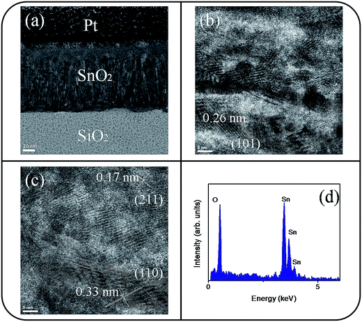 |
| | Fig. 4 TEM analyses of the SnO2 thin film: (a) low-magnification TEM image of the film. (b) and (c) HRTEM images taken from the local regions of the film. (d) EDS spectra of Sn, and O elements taken from the film. | |
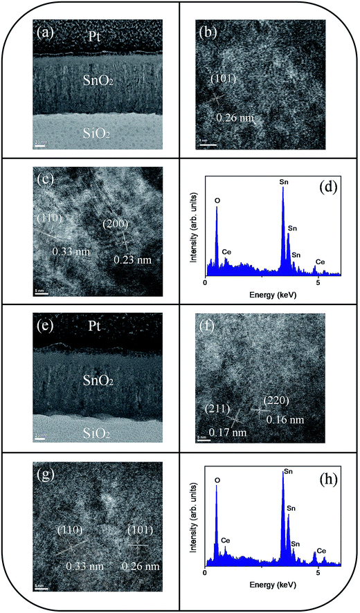 |
| | Fig. 5 TEM analyses of the Ce-doped SnO2 thin film prepared at 40 W: (a) low-magnification TEM image of the film. (b) and (c) HRTEM images taken from the local regions of the film. (d) EDS spectra of Sn, Ce, and O elements taken from the film. TEM analyses of the Ce-doped SnO2 thin film prepared at 60 W: (e) low-magnification TEM image of the film. (f) and (g) HRTEM images taken from the local regions of the film. (h) EDS spectra of Sn, Ce, and O elements taken from the film. | |
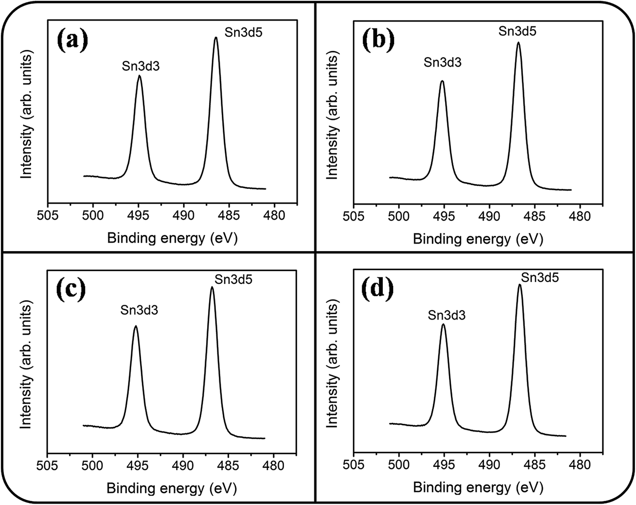
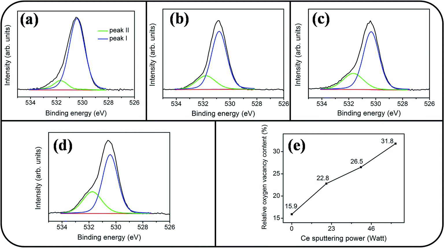
Fig. 6(a)–(d) show a symmetric Sn 3d5/2 peak centered at approximately 486 eV and a Sn 3d3/2 peak centered at approximately 495 eV; no signal from the metallic Sn was observed. The analysis of XPS narrow scans of the Sn 3d core-level doublet indicated that the Sn4+ valence state existed in the form of SnO2.30 Fig. 7(a)–(c) depict the Ce 3d XPS spectra of the SnO2 thin films doped with various concentrations of Ce. Notably, the Ce 3d spectrum intensity increased and became substantially visible with an increase in the Ce concentration in the SnO2 thin film. Moreover, a visible five-peak feature in the Ce 3d XPS spectra was observed in the Ce-doped SnO2 thin films prepared using Ce sputtering powers of 40 and 60 W. The Ce 3d XPS spectra can be divided into two series of subpeaks according to the Ce 3d spin–orbit states, as illustrated in Fig. 7(b) and (c); eight Gaussian deconvolution subpeaks corresponding to Ce3+ (red peaks) and Ce4+ (blue peaks) were used to fit the Ce 3d XPS spectra.31 The Ce ions in the SnO2 thin films clearly exhibited a mixed valence state. The cerium concentrations of the Ce-doped SnO2 thin films with various Ce sputtering powers were evaluated through XPS analyses, and the concentrations were 1.2, 2.3, and 4.5 at% for the Ce sputtering powers of 20, 40, and 60 W, respectively. Fig. 8(a)–(d) depict the XPS spectra of O 1s for the undoped and Ce-doped SnO2 thin films synthesized using various Ce sputtering powers. The O 1s spectra have an asymmetric curve feature. Two Gaussian curves fit the O 1s spectra, and they are centered at approximately 530.5 (peak I) and 531.8 eV (peak II), which are associated, respectively, with the oxygen ions in the tin oxide film and an oxygen vacancy within the tin oxide lattice.32 The relative size of the peak at high binding energy increased gradually with an increase in Ce sputtering power for the film, indicating that the oxygen vacancy content of the Ce-doped SnO2 thin films increased with Ce concentration. The relative oxygen vacancy content in the crystalline undoped and Ce-doped SnO2 thin films was evaluated according to the following intensity ratio of these two Gaussian deconvolution peaks: (peak I)/(peak I + peak II).30,33 Fig. 8(e) summarizes the change in the relative oxygen vacancy content of the SnO2 thin films grown with and without various Ce sputtering powers. The oxygen vacancy content increased from 15.9% to 31.8% as the Ce sputtering power increased to 60 W. The relevant ionic radii (Sn4+ = 0.069 nm, Ce3+ = 0.103 nm, and Ce4+ = 0.096 nm) differed substantially between Ce and Sn ions.34–36 The partial substitution of Sn4+ by Ce3+ and Ce4+ in the SnO2 crystallites further caused the formation of oxygen vacancy defects in the SnO2 lattices. The increased number of oxygen vacancy defects in impurity-doped oxides, because of differences in radii between the doping ions and parent ions, has been observed in In-doped ZnO films and Al-doped SnO2 nanotubes.37,38
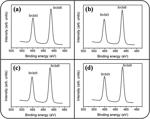 |
| | Fig. 6 XPS narrow scans of Sn 3d core level doublet of the Ce-doped SnO2 thin films prepared at various Ce sputtering powers: (a) 0 W, (b) 20 W, (c) 40 W, (d) 60 W. | |
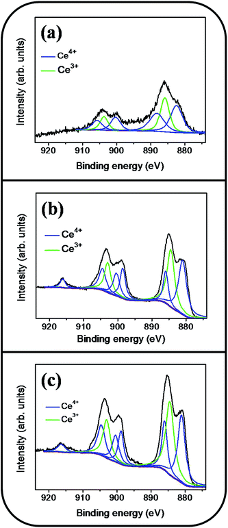 |
| | Fig. 7 Ce 3d XPS narrow scan spectra of the Ce-doped SnO2 thin films prepared at various Ce sputtering powers: (a) 20 W, (b) 40 W, (c) 60 W. | |
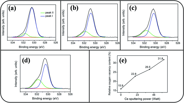 |
| | Fig. 8 XPS narrow scans of O 1s core level of the Ce-doped SnO2 thin films prepared at various Ce sputtering powers: (a) 0 W, (b) 20 W, (c) 40 W, (d) 60 W. (e) Relative oxygen vacancy content vs. Ce sputtering power of the Ce-doped SnO2 films. | |
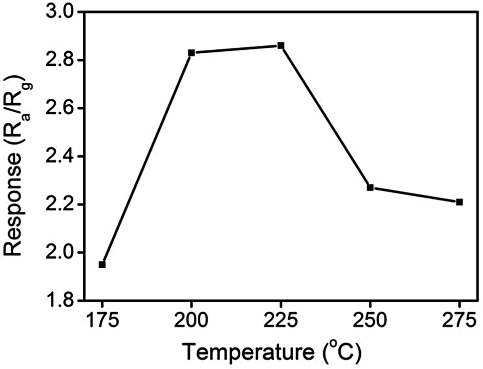
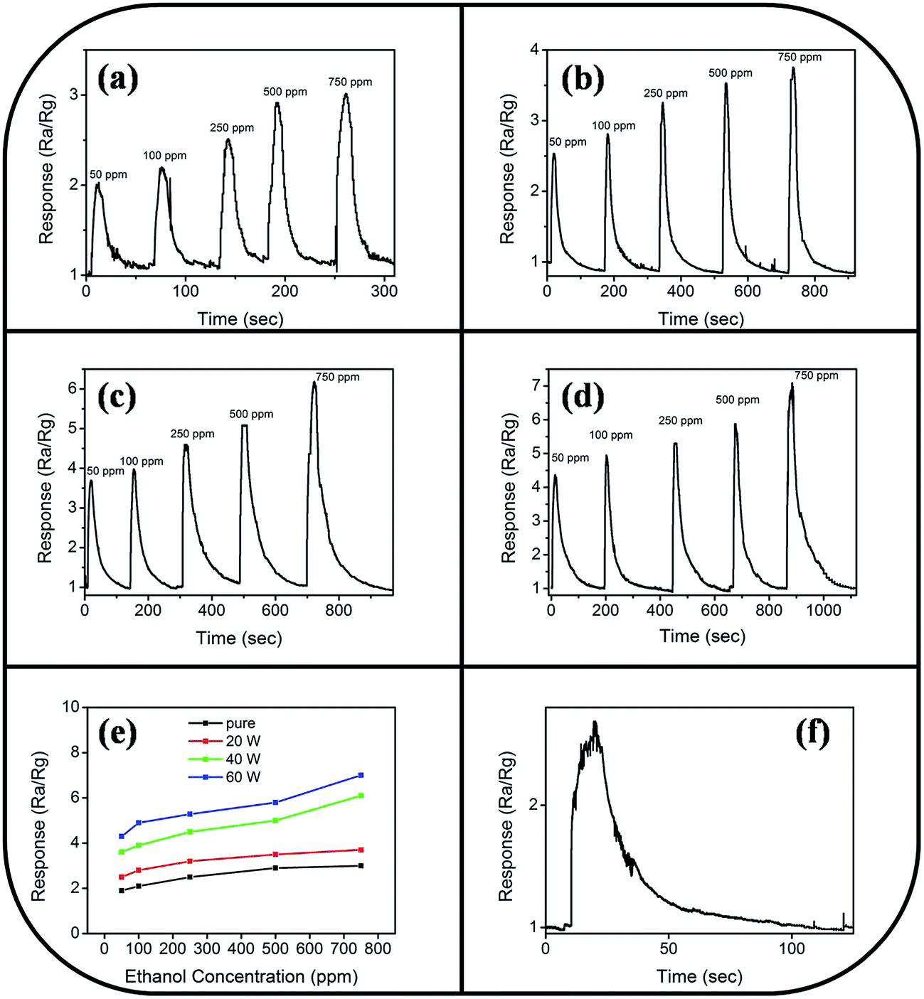
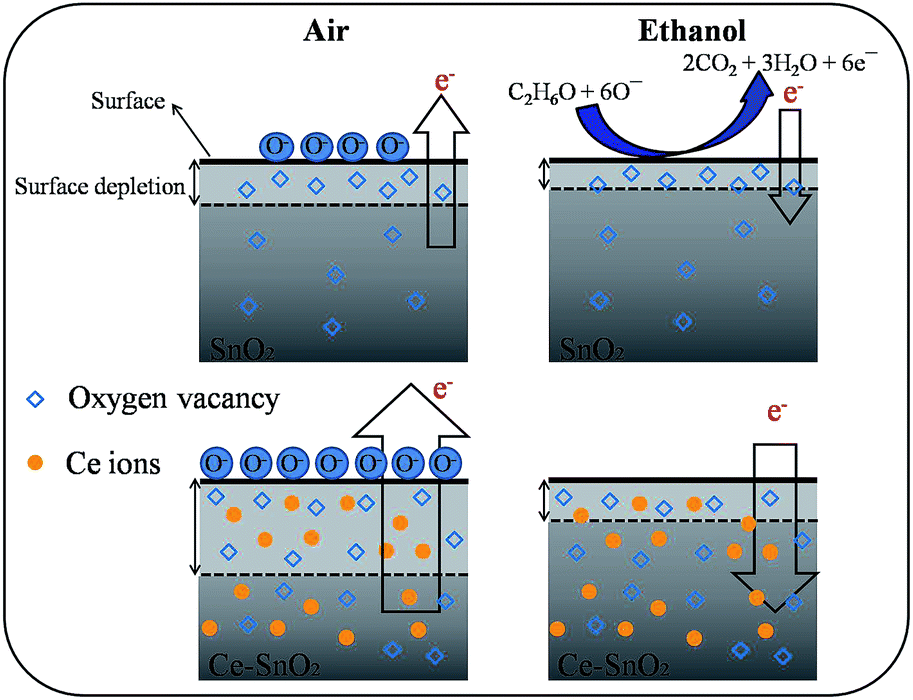
Fig. 9 illustrates the variation of gas-sensing responses of the SnO2 thin film at the various operating temperatures on exposure to ethanol vapor at 500 ppm. The gas-sensing response of the SnO2 thin film reached the maximum value at 225 °C and exhibited a decrease above that operating temperature. The changes in gas-sensing responses of the SnO2 thin film with operating temperature are attributable to the fact that the adsorption of oxygen molecules onto the surfaces of the SnO2 thin film is a chemisorptive behavior at elevated temperatures. The optimal operating temperature of oxide thin-film sensors depends on the balance between the temperature-related chemical reactions and gas diffusion speed.19 The operating temperature-dependent gas-sensing response of the SnO2 thin film in this work revealed that both surface reaction with ethanol vapor and the diffusion of ethanol vapor to the surface of the thin film reached an equilibrium at 225 °C; therefore, the gas-sensing response of the SnO2 thin film reaches a maximum value at this temperature. Fig. 10(a)–(d) depict the typical dynamic gas-sensing response curves of undoped and Ce-doped SnO2 thin films toward various concentrations of ethanol vapor (50, 100, 250, 500, and 750 ppm). The gas-sensing behaviors of the undoped and Ce-doped SnO2 thin films on exposure to ethanol vapor were visibly different. This is due to the n-type nature of SnO2, which reduced the electrical resistance of the undoped and Ce-doped SnO2 thin films on exposure to ethanol vapor; the resistance returned completely to the initial state on removal of the vapor. The adsorbed oxygen molecules on the surfaces of the SnO2 thin film extracted electrons from the conduction band of the SnO2 and formed surface-adsorbed oxygen ions. Further introducing the ethanol vapor into the gas-sensing test chamber caused the surface of SnO2 thin film to readily react with the oxygen ions and liberate electrons to the conduction band; these effects were accompanied by an increase in conductivity of the SnO2 thin film according to the following reaction: C2H6O + 6Oad− = 2CO2 + 3H2O + 6e−.39,40 Fig. 10(e) summarizes the gas-sensing response values of the undoped and Ce-doped SnO2 thin films to various concentrations of ethanol vapor. Notably, the gas-sensing response of the SnO2 thin film was enhanced through Ce doping. The gas-sensing responses of undoped SnO2 thin films were 1.9, 2.1, 2.5, 2.9, and 3.2 at ethanol vapor concentrations of 50, 100, 250, 500, and 750 ppm, respectively. The gas-sensing responses of the Ce-doped the SnO2 thin film prepared using a Ce sputtering power of 20 W increased to 2.5, 2.8, 3.2, 3.5, and 3.7 at ethanol vapor concentrations of 50, 100, 250, 500, and 750 ppm, respectively. From the aforementioned composition analysis, adding a trace amount of Ce (1.2 at%) into the SnO2 thin film engendered slight improvement of the gas-sensing response of the SnO2 thin film toward ethanol vapor. On further increasing the Ce concentration in the SnO2 thin films, a substantial enhancement of the gas-sensing response was observed for the SnO2 thin films with a Ce concentration higher than 2.3 at%. The Ce-doped SnO2 thin films prepared using a Ce sputtering power of 60 W contained approximately 4.5 at% Ce and exhibited the highest gas-sensing responses toward the ethanol vapor concentrations of 50–750 ppm. Notably, employing a Ce sputtering power higher than 60 W did not increase the gas-sensing response of the Ce-doped SnO2 thin film further. Employing a Ce sputtering power of 80 W reduced the gas-sensing response of the Ce-doped SnO2 thin film to approximately 2.6 on exposure to ethanol vapor at 500 ppm (Fig. 10(f)). This result indicated that the gas-sensing response increased with an increase in Ce concentration in the SnO2 thin films below 4.5 at%; this Ce concentration represented an optimal value in the SnO2 thin film for obtaining superior ability to detect ethanol vapor in the present work. The possible reason for the decreased gas-sensing sensitivity of the Ce-doped SnO2 thin film prepared at 80 W Ce sputtering power might be associated with the deteriorated crystalline quality of the SnO2 thin film under Ce doping at a relatively high sputtering power; this is supported by the XRD pattern with the markedly decreased intensity and broadened full-width at half-maximum of SnO2 Bragg reflections (ESI†). The responses and recovery times of undoped and Ce-doped SnO2 thin films were defined as the durations required for the occurrence of a 90% change in resistance upon exposure to ethanol vapor (response) and to air (recovery), respectively.41 The response times of undoped and various Ce-doped SnO2 thin films on exposure to various ethanol vapor concentrations (50–750 ppm) were prompt and in the range of 4–8 s. No marked differences in response time were observed among the various thin-film samples. By contrast, the recovery times of the Ce-doped SnO2 thin films with various Ce concentrations were in the range 43–135 s, whereas those of the undoped SnO2 layers were in the range 30–41 s. The fact that the recovery time was longer than the response time of the thin-film samples in this study revealed that the desorption reaction of oxygen ions with ethanol vapor molecules in the sensing-response process is faster than the adsorption of oxygen molecules from air in the sensing-recovery process.39 Furthermore, increased adsorption sites on the surface of the Ce-doped SnO2 thin film might have caused it to require a longer duration to completely readsorb oxygen molecules from ambient air onto the thin-film surface reaction sites; therefore, longer recovery times were observed in the Ce-doped SnO2 thin films than in the undoped SnO2 thin films. Table 1 summarized gas-sensing performance of other metal-doped SnO2 thin films prepared by various methods.42–45 Comparatively, the 4.5 at% Ce-doped SnO2 thin films herein is of potential for applications in detecting ethanol vapor. The enhanced gas-sensing responses of the SnO2 thin films through moderate Ce doping were attributable to the factors associated with their microstructures and Ce ions in the films. Fig. 11 illustrates the possible mechanism for the higher gas-sensing response of Ce-doped SnO2 than that of undoped SnO2 in this study. From the aforementioned XPS results, the cosputtering growth of Ce-doped SnO2 thin films indicated a coexistence of Ce3+ and Ce4+ ions in the film. Moreover, the amount of Ce4+ ions and oxygen vacancy in the SnO2 thin films increased with an increase in the Ce concentration. The oxygen vacancies are posited to be favorable adsorption sites in oxide surfaces for oxygen molecules. Recent work on Al-doped SnO2 has shown that doping SnO2 with Al engenders oxygen vacancies at the surface of SnO2, which facilitates oxygen adsorption and the formation of surface catalytic active O−–O−; thus, the gas response is markedly enhanced.38 Furthermore, Ce4+ ions have been shown to exhibit satisfactory catalytic behavior toward oxygen molecules.14 The Ce4+ ions near the surface of the Ce-doped SnO2 thin films can promote charge transfer of the surface-adsorbed oxygen molecules, thereby further increasing the number of adsorbed oxygen ions on the surface of the Ce-doped SnO2 thin films. An increased Ce concentration in the SnO2 thin films also engendered the roughening of the SnO2 film surface. These factors are beneficial because they caused a relatively large number of oxygen ions to be adsorbed on the Ce-doped SnO2 prepared with a Ce sputtering power of 60 W in this study. Therefore, it is reasonable to assume that the surface depletion layer of the Ce-doped SnO2 thin film is thicker than that of the SnO2 thin film on exposure to ambient air because of the larger number of adsorbed oxygen ions on the Ce-doped SnO2 thin film surface. By comparison, when the ethanol gas was introduced into the test chamber, a higher degree of depletion thickness variation of the Ce-doped SnO2 was expected because a higher number of surface adsorbed oxygen ions would react with ethanol gas molecules. A larger variation of the depletion thickness of the Ce-doped SnO2 thin films engendered a larger variation in electric resistance on exposure to the ethanol vapor. Therefore, the gas-sensing responses of the Ce-doped SnO2 thin film prepared using a Ce sputtering power of 60 W were superior to those of the undoped SnO2 thin film and SnO2 thin films prepared using Ce sputtering powers of 20 and 40 W.
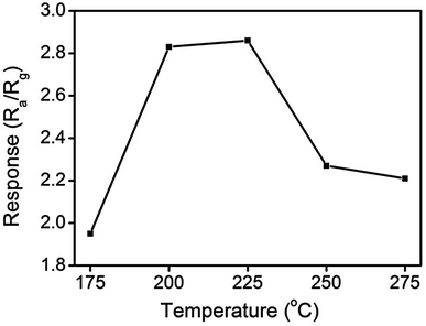 |
| | Fig. 9 Gas sensing response value vs. operating temperature of the SnO2 thin film. | |
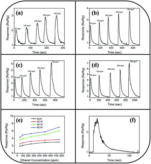 |
| | Fig. 10 Gas sensing response curves of the Ce-doped SnO2 films prepared at various Ce sputtering powers on exposure to various concentrations of ethanol vapor (50, 100, 250, 500, and 750 ppm): (a) 0 W, (b) 20 W, (c) 40 W, (d) 60 W. (e) Gas sensing response values vs. ethanol vapor concentrations for various Ce-doped SnO2 films. (f) Gas sensing response curve of the Ce-doped SnO2 film prepared at 80 W Ce sputtering power on exposure to 500 ppm ethanol vapor. | |
Table 1 Comparisons of gas-sensing performances of various metal-doped SnO2 thin films. (Ra is the sensor electrical resistance in the absence of target gas and Rg is that in the target gas)
| Materials |
Deposition technique |
Target gas |
Operating temperature |
S: sensor response |
Response time (s) |
Recovery time (s) |
Ref. |
| W-Doped SnO2 thin film |
Spray pyrolysis |
NO2 |
225 °C |
132 (400 ppm) |
2 |
25 |
42 |
| S = [(Rg − Ra)/Ra] × 100 |
| Cu-Doped SnO2 thin film |
Cosputtering |
Ethanol |
180 °C |
∼4 (100 ppm) |
140 |
N/A |
43 |
| S = Ra/Rg |
| Ru-Doped SnO2 thin film |
Spray pyrolysis |
Ethanol |
250 °C |
87.2 (100 ppm) |
N/A |
N/A |
44 |
| S = [(Ra − Rg)/Ra] × 100 |
| Pt-Doped SnO2 thin film |
Spray pyrolysis |
CO |
300 °C |
12 (200 ppm) |
N/A |
N/A |
45 |
| S = Ra/Rg |
| Ce-Doped SnO2 thin film |
Cosputtering |
Ethanol |
225 °C |
5 (100 ppm) |
4 |
45 |
This work |
| S = Ra/Rg |
 |
| | Fig. 11 A schematic of gas sensing mechanisms for the undoped and Ce-doped SnO2 thin film on exposure to ethanol vapor. The size of black arrows represented the number of electrons extracted by adsorbed oxygen molecules and liberated from adsorbed oxygen ions. | |
Conclusions
Ce-Doped SnO2 thin films with various cerium concentrations were prepared using cosputtering of Sn and Ce metallic targets with different Ce sputtering powers. The as-prepared Ce-doped SnO2 thin films contained cerium in the concentration range 1.2–4.5 at% and exhibited a columnar grain feature with a high crystallinity. The surface roughness of the Ce-doped SnO2 thin films increased with the cerium concentration in the films. Increasing the Ce sputtering power led to the formation of an increased number of oxygen vacancies and Ce4+ ions near the Ce-doped SnO2 thin film surface. The increased number of oxygen vacancies and Ce4+ ions and surface roughness of the 4.5 at% Ce-doped SnO2 thin films prepared using a relatively high Ce sputtering power considerably improved the ethanol-gas-sensing responses of the films.
Acknowledgements
This work is supported by the Ministry of Science and Technology of Taiwan (Grant No. MOST 105-2628-E-019-001-MY3).
References
- Y. Li, L. Qiao, L. Wang, Y. Zeng, W. Fu and H. Yang, Appl. Surf. Sci., 2013, 285, 130–135 CrossRef CAS.
- N. Bhardwaj and S. Mohapatra, Ceram. Int., 2016, 42, 17237–17242 CrossRef CAS.
- G. Singh, R. Thangaraj and R. C. Singh, Ceram. Int., 2016, 42, 4323–4332 CrossRef CAS.
- W. X. Jin, S. Y. Ma, Z. Z. Tie, W. Q. Li, J. Luo, L. Cheng, X. L. Xu, T. T. Wang, X. H. Jiang and Y. Z. Mao, Appl. Surf. Sci., 2015, 353, 71–78 CrossRef CAS.
- Y. Shen, X. Cao, B. Zhang, D. Wei, J. Ma, W. Liu, C. Han and Y. Shen, J. Alloys Compd., 2014, 593, 271–274 CrossRef CAS.
- E. M. El-Maghraby, A. Qurashi and T. Yamazaki, Ceram. Int., 2013, 39, 8475–8480 CrossRef CAS.
- S. Agarwala, W. L. Ong and G. W. Ho, Sci. Adv. Mater., 2013, 5, 1418–1426 CrossRef CAS.
- K. Govardhan and A. N. Grace, J. Sens., 2016, 7652450 Search PubMed.
- Y. Qu, H. Wang, H. Chen, J. Xiao, Z. Linb and K. Dai, RSC Adv., 2015, 5, 16446–16449 RSC.
- L. K. Bagal, J. Y. Patil, M. V. Vaishampayan, I. S. Mulla and S. S. Suryavanshi, Sens. Actuators, B, 2015, 207, 383–390 CrossRef CAS.
- L. K. Bagal, J. Y. Patil, I. S. Mulla and S. S. Suryavanshi, Ceram. Int., 2012, 38, 6171–6179 CrossRef CAS.
- W. Q. Li, S. Y. Ma, Y. F. Li, X. B. Li, C. Y. Wang, X. H. Yang, L. Cheng, Y. Z. Mao, J. Luo, D. J. Gengzang, G. X. Wan and X. L. Xu, J. Alloys Compd., 2014, 605, 80–88 CrossRef CAS.
- P. Baraneedharan, S. Imran Hussain, V. P. Dinesh, C. Siva, P. Biji and M. Sivakumar, Appl. Surf. Sci., 2015, 357, 1511–1521 CrossRef CAS.
- D. Liu, T. Liu, H. Zhang, C. Lv, W. Zeng and J. Zhang, Mater. Sci. Semicond. Process., 2012, 15, 438–444 CrossRef CAS.
- F. M. Li, X. B. Li, S. Y. Ma, L. Chen, W. Q. Li, C. T. Zhu, X. L. Xu, Y. Chen, Y. F. Li and G. Lawson, J. Alloys Compd., 2015, 649, 1136–1144 CrossRef CAS.
- D. Han, P. Song, S. Zhang, H. Zhang, Q. Xu and Q. Wang, Sens. Actuators, B, 2015, 216, 488–496 CrossRef CAS.
- P. Mohanapriya, H. Segawa, K. Watanabe, K. Watanabe, S. Samitsu, T. S. Natarajan, N. V. Jaya and N. Ohashi, Sens. Actuators, B, 2013, 188, 872–878 CrossRef CAS.
- Y. C. Liang and X. S. Deng, Ceram. Int., 2014, 40, 1687–1692 CrossRef CAS.
- Y. C. Liang, Y. R. Cheng, H. Y. Hsia and C. C. Chung, Appl. Surf. Sci., 2016, 364, 837–842 CrossRef CAS.
- J. Kaur, V. D. Vankar and M. C. Bhatnagar, Sens. Actuators, B, 2008, 133, 650–655 CrossRef CAS.
- S. Agarwala, Z. H. Lim, E. Nicholson and G. W. Ho, Nanoscale, 2012, 4, 194–205 RSC.
- S. Chen, X. Zhao, H. Xie, J. Liu, L. Duan, X. Ba and J. Zhao, Appl. Surf. Sci., 2012, 258, 3255–3259 CrossRef CAS.
- Y. C. Liang, M. Y. Tsai, C. L. Huang, C. Y. Hu and C. S. Hwang, J. Alloys Compd., 2011, 509, 3559–3565 CrossRef CAS.
- J. W. H. van Krevel, H. T. Hintzen and R. Metselaar, Mater. Res. Bull., 2000, 35, 747–754 CrossRef CAS.
- J. H. Lee and B. O. Park, Thin Solid Films, 2003, 426, 94–99 CrossRef CAS.
- E. Gungor, T. Gungor, D. Caliskan, A. Ceylan and E. Ozbay, Appl. Surf. Sci., 2014, 318, 309–313 CrossRef CAS.
- H. J. Lin, T. S. Yang, C. S. Hsi, M. C. Wang and K. C. Lee, Ceram. Int., 2014, 40, 10633–10640 CrossRef CAS.
- Y. C. Liang, H. Zhong and W. K. Liao, Nanoscale Res. Lett., 2013, 8, 345 CrossRef PubMed.
- Y. C. Liang and H. Y. Lee, CrystEngComm, 2010, 12, 3172–3176 RSC.
- Y. C. Liang and H. Zhong, Nanoscale Res. Lett., 2013, 8, 358 CrossRef PubMed.
- S. Somacescu, R. Scurtu, G. Epurescu, R. Pascu, B. Mitu, P. Osiceanu and M. Dinescu, Appl. Surf. Sci., 2013, 278, 146–152 CrossRef CAS.
- Y. C. Liang, C. Y. Hu and H. Zhong, Appl. Surf. Sci., 2012, 261, 633 CrossRef CAS.
- Y. C. Liang and X. S. Deng, J. Alloys Compd., 2013, 569, 144–149 CrossRef CAS.
- Y. Zhao, J. Liu, L. Shi, S. Yuan, J. Fang, Z. Wang and M. Zhang, Appl. Catal., B, 2011, 103, 436–443 CrossRef CAS.
- Y. Yokota, A. Yamaji, S. Kurosawa, K. Kamada and A. Yoshikawa, Opt. Mater., 2014, 36, 1950–1953 CrossRef CAS.
- C. Ge, C. Xie and S. Cai, Mater. Sci. Eng., B, 2007, 137, 53–58 CrossRef CAS.
- Y. C. Liang and C. M. Lee, J. Appl. Phys., 2016, 120, 135306 CrossRef.
- J. Wu, Q. Huang, D. Zeng, S. Zhang, L. Yang, D. Xia, Z. Xiong and C. Xie, Sens. Actuators, B, 2014, 198, 62–69 CrossRef CAS.
- Y. C. Liang, S. L. Liu and H. Y. Hsia, Nanoscale Res. Lett., 2015, 10, 350 CrossRef PubMed.
- Y. C. Liang and S. L. Liu, Acta Mater., 2015, 88, 245–251 CrossRef CAS.
- Y. C. Liang, W. K. Liao and X. S. Deng, J. Alloys Compd., 2014, 599, 87–92 CrossRef CAS.
- M. Kumar, A. Kumar and A. C. Abhyankar, ACS Appl. Mater. Interfaces, 2015, 7, 3571–3580 CAS.
- S. Zhang, P. Zhang, Y. Wang, Y. Ma, J. Zhong and X. Sun, ACS Appl. Mater. Interfaces, 2014, 6, 14975–14980 CAS.
- C. Sankar, V. Ponnuswamy, M. Manickam, R. Mariappan and R. Suresh, Appl. Surf. Sci., 2015, 349, 931–939 CrossRef CAS.
- T. V. K. Karthik, M. d. l. L. Olvera, A. Maldonado and V. Velumurugan, Mater. Sci. Semicond. Process., 2015, 37, 143–150 CrossRef CAS.
Footnote |
| † Electronic supplementary information (ESI) available. See DOI: 10.1039/c6ra25853k |
|
| This journal is © The Royal Society of Chemistry 2017 |
Click here to see how this site uses Cookies. View our privacy policy here. 
 Open Access Article
 This Open Access Article is licensed under a
  *,
Chia-Min Lee and
Ya-Ju Lo
*,
Chia-Min Lee and
Ya-Ju Lo