
 Open Access Article
 This Open Access Article is licensed under a Creative Commons Attribution-Non Commercial 3.0 Unported Licence
Mechanism of enhancing visible-light photocatalytic activity of BiVO4 via hybridization of graphene based on a first-principles study
Yuxuan Chena,
Xinguo Ma*ab,
Di Lic,
Huihu Wangb and
Chuyun Huang*ab
aSchool of Science, Hubei University of Technology, Wuhan 430068, China. E-mail: maxg2013@sohu.com
bHubei Collaborative Innovation Center for High-efficiency Utilization of Solar Energy, Hubei University of Technology, Wuhan 430068, China. E-mail: chuyunh@163.com
cSchool of Metallurgical Engineering, Xi’an University of Architecture and Technology, Xi’an 710055, China
First published on 12th December 2016
Abstract
The interface properties of the hybrid graphene/BiVO4(001) heterojunction were investigated by first-principle calculations incorporating semiempirical dispersion-correction schemes to correctly describe van der Waals interactions. The results indicate that graphene and BiVO4 are in contact and form a stable heterojunction. After equilibration of the graphene/BiVO4 interface, their energy levels are adjusted with the shift of their Fermi levels based on calculated work functions. In addition, electrons in the upper valence band of BiVO4 can be excited to the conduction band under irradiation, and then arrive at the C pz orbital of graphene, in which the electrons cannot migrate back to BiVO4 and thus are trapped in graphene. Thus, substantial holes are accumulated in the BiVO4(001) surface, facilitating the separation of photogenerated e−/h+ pairs. The calculated charge density difference unravels that the charge redistribution drives the interlayer charge transfer from graphene to the BiVO4(001) surface. It is identified that the hybridization between the two components induces an increase of optical absorption of BiVO4 in the visible-light region. A deep understanding of the microcosmic mechanisms of interface interaction and charge transfer in this system would be helpful for fabricating BiVO4-based heterojunction photocatalysts.
Introduction
Bismuth vanadate (BiVO4) is one of the most promising photocatalytic materials for O2 evolution from water-splitting, and the degradation of organics under visible-light irradiation.1,2 It is well known that BiVO4 has three main crystalline phases: scheelite-monoclinic (sm-BiVO4), scheelite-tetragonal (st-BiVO4) and zircon-tetragonal (zt-BiVO4).1 Among them, sm-BiVO4 with a band gap of 2.4 eV and a valence band (VB) edge at approximately 2.5 V vs. NHE is the most common phase under ambient conditions and exhibits the highest photocatalytic activity under visible-light irradiation.3–6 Various successful modifications have been made to improve the photocatalytic and photoelectrochemical activity of BiVO4 using the following techniques: controlling morphologies,7–9 doping,10,11 and coupling with metal oxide semiconductors12,13 or carbon materials.14 Among the above mentioned strategies, coupling with a different semiconductor or metal to match their energy levels is an effective method to separate charges using internal polarization and charged surfaces, but the importance of these phenomena in BiVO4 have not yet been fully explored.15,16In the reported systems of heterostructured photocatalysts, it is accepted that interface properties of heterojunctions are critical for determining the final photocatalytic activity of the systems.17–19 Interface properties can be attributed to two important aspects: one is the lattice match between the two components, which is the prerequisite for fabricating heterojunctions; the other is the suitable conduction band (CB) and/or VB levels, considered to be the prime and fundamental requirement for charge transfer and separation in heterostructured interfaces. It is well known that graphene is an electron collector and transporter, and may be used to boost the performance of various energy conversion and storage devices,20,21 or to be a dispersible carrier for catalysts.22 The uniqueness of this two-dimensional crystal, i.e., high carrier mobility, make it a dopant with the purpose of manipulating the electronic structure of BiVO4, and thus facilitates the enhancement of the carrier mobility, namely, metal-like electroconductivity.
The graphene/BiVO4 systems successfully prepared via a one-step hydrothermal method without the use of any surfactants show superior photoactivity in the degradation of MB, RhB, MO and active black BLG under visible-light irradiation.14 Considering the large specific surface area, the combination of BiVO4 and graphene effectively inhibits the aggregation of these nanoparticles and consequently gives rise to a higher photocatalytic performance.14,23 It is noted that sm-BiVO4 nanoplates (space group: I2/b) with exposed (001) facets exhibit greatly enhanced photocatalytic activity9,24,25 and the rate of oxygen evolution increases with the area of the (001) surface under visible-light irradiation.24 A higher drift velocity of carriers in the (001) direction would bring more of the majority carrier to the (001) surface and promote reduction.25 However, compared with the progress in experimental fabrication of graphene/BiVO4(001) heterojunctions, its underlying characteristics of the interaction from a theoretical point of view are still far from being explained. Thus, complementary to previous experimental results, in this work, much effort was made to study the basic mechanisms of interface interaction, charge transfer and separation, and optical properties through density functional theory (DFT) calculations. We finally present a coherent picture of the interface properties, which provides a necessary reference for further optimizing the performance of heterojunctions.
Calculation methods
All calculations were performed using the ultrasoft pseudopotentials (USP) with the exchange and correlation in the Perdew–Burke–Ernzerhof (PBE)26 and Ceperley–Alder (CA)27 formalisms of density functional theory as implemented in the CASTEP code. In USP calculations, a pragmatic method to correctly describe van der Waals (vdW) interactions resulting from dynamical correlations between fluctuating charge distributions was taken by the Grimme method.28 And a hybrid semiempirical solution from Ortmann, Bechstedt and Schmidt (OBS) was also given to introduce damped atom pair wise dispersion corrections of the form C6R6− in the DFT formalism.29 The total energy (Etotal) is represented as:| Etotal = EKS-DFT + EvdW | (1) |
Results and discussion
Structural stability
Before exploring the properties of the graphene/BiVO4 heterojunction, we first investigated the crystal structures of single-layer graphene, bulk BiVO4, and the BiVO4(001) surface. Our optimized lattice parameters for graphene (a = b = 2.458 Å, α = 90.013°) and bulk BiVO4 (space group: I2/b, a = 5.182 Å, b = 5.139 Å, c = 11.757 Å, α = 89.876°) are in agreement with experimental values.31 It is worthwhile to mention that the I/2b space group can be converted to C2/c.15 Since both I2/b and C2/c space groups, which have different unit cell choices and crystallographic axes, are commonly used to describe the scheelite-monoclinic structure of BiVO4, it is necessary to clarify the space group used when referring to specific atomic planes or crystal directions as well as the hkl indices of X-ray diffraction peaks in order to prevent any possible confusion. In fact, it can be inferred clearly that the (001) surface for the I2/b space group is equivalent to the (010) surface for the C2/c space group.15Depending on where the surface is sliced, there are two different structures of the BiVO4(001) surface with the same number of surface dangling bonds (1 × 1 slab with four dangling bonds), as shown in Fig. 1a. It is well known that the number of ionic layers and the width of vacuum space play crucial roles in the accuracy of the calculations of the atomic relaxation and the electronic properties. A vacuum layer of 10 Å is used to isolate the slab as the boundary condition, which according to other previous work, is good enough to make interactions between neighbouring slabs negligible. Dependence of surface energies on slab thickness presents an oscillating odd–even behavior, as shown in Fig. 1b. The surface energies of slabs with an odd number of layers (model 2) are higher because they have an additional symmetry plane at the slab center, so the atomic displacements on both sides of the slab are mirrored and tend to reinforce each other. It is found that the slabs of the BiVO4(001) surface with an even number of layers (model 1) are energetically more favorable than those with an odd number of layers within the GGA-PBE or LDA-CA formalism. Thus, it can be inferred from Fig. 1 that the ideal 1 × 1 slab of the BiVO4(001) surface exposes two 2-fold undercoordinated O atoms, a 6-fold undercoordinated Bi atom and a fully 4-fold coordinated V atom. Comparing with our final value of surface energy, the surface energies of the 6-layer slab only result in an error of −4.5%. So the model of the 6-layer slab is sufficient to present the geometry structure and electronic properties of the BiVO4(001) surface.
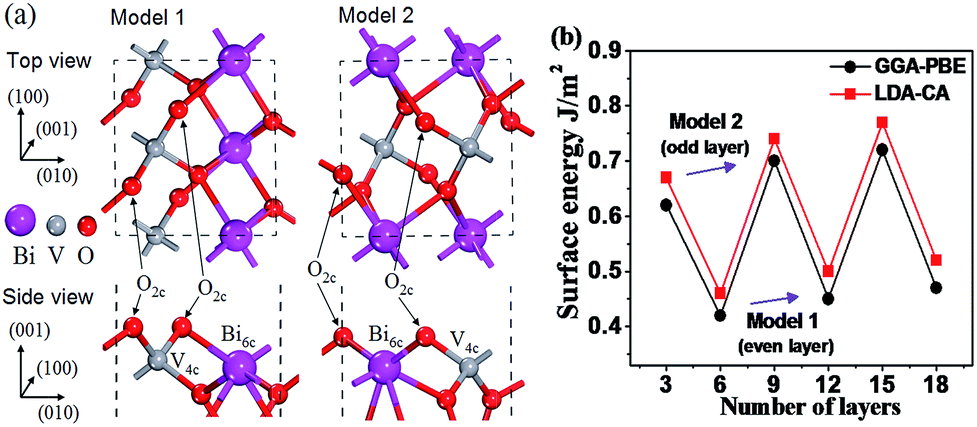 | ||
| Fig. 1 (a) Top and side views of model 1 (even layer) and model 2 (odd layer) for the BiVO4(001) surface. (b) Surface energies (J m−2) of the BiVO4(001) surface as a function of slab thickness with a 10 Å vacuum within the GGA-PBE and LDA-CA formalism, respectively. Surface energy is defined as follows: Esurf = (Eslab − NEbulk)/2A, where Eslab and Ebulk are the total energies for the slabs (containing N units for the primitive cell) and for the bulk crystal (a primitive cell), respectively; 2A is used, as the total area of two equivalent surfaces in the slab model. | ||
To further examine the interaction between graphene and BiVO4(001), based on the TEM and SEM result of graphene/BiVO4 heterojunctions,32 the graphene/BiVO4(001) interface is modeled by using a supercell slab, in which the geometry structure contains parallel graphene and BiVO4(001) sheets. A 2 × 5 (following the conventional definition of the zigzag/armchair nanoribbon) graphene layer containing 40 carbon atoms was chosen as the substrate to support a 1 × 4 BiVO4(001) surface containing 8Bi, 8V and 32O atoms, as shown in Fig. 2. The whole system contained 88 atoms with 496 valence electrons. The mismatch of initial lattice parameters between the optimized graphene and BiVO4(001) sheets is only 1.6% using the Grimme scheme and 1.8% using the OBS scheme, which are larger than that of the graphene@MoSe2 interface33 and slightly smaller than that of the graphene@diamond interface.34 In subsequent work, the Grimme schemes are taken to deal with the vdW interactions in the graphene/BiVO4(001) interface.
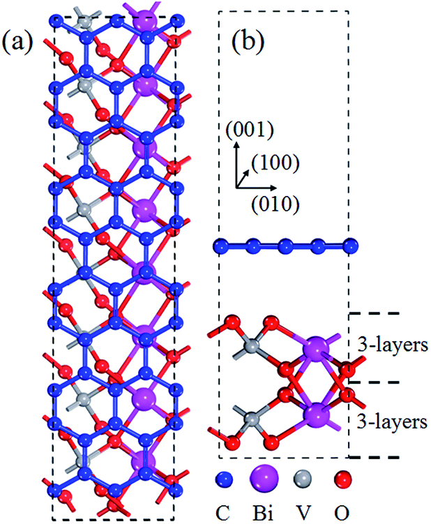 | ||
| Fig. 2 Top (a) and side (b) views of optimized geometric structures of the graphene/BiVO4(001) heterojunction. | ||
To investigate the thermodynamic stability of the graphene/BiVO4(001) heterojunction, the interface adhesion energy was obtained according to the following equation:33–35
| E(ad) = E(hetero) − E(graphene) − E(BiVO4(001)) | (2) |
| ΔEmismatch = E(BiVO4(001))a′ + E(graphene)a′ − E(BiVO4(001))a1 + E(graphene)a2 | (3) |
Electronic structure
To understand the effect of the orbital hybridization on electronic structure of the interface, we calculated the energy band structures of the graphene/BiVO4(001) heterojunction using the GGA-PBE method. For the purposes of comparison, the energy bands of isolated graphene, bulk BiVO4 and the BiVO4(001) surface were also calculated. The energy band structures, drawn along high symmetry lines of the Brillouin zone, are shown in Fig. 3. The calculated results show that the graphene is a gapless semiconductor, the (bonding) π bands and (antibonding) π* bands cross only at the corners of the hexagonal Brillouin zone of the system, the so-called K points. A direct band gap of 2.17 eV for bulk BiVO4 is 0.23 eV smaller than the experimental value previously reported by Li et al.,5 due to the well-known limitation in DFT calculations. However, it is noted that the band gap of the BiVO4(001) sheet was calculated to be 2.52 eV, which is very close to the experimental measurement of 2.54 eV using UV-vis absorbance spectroscopy for BiVO4(001) nanoplates.9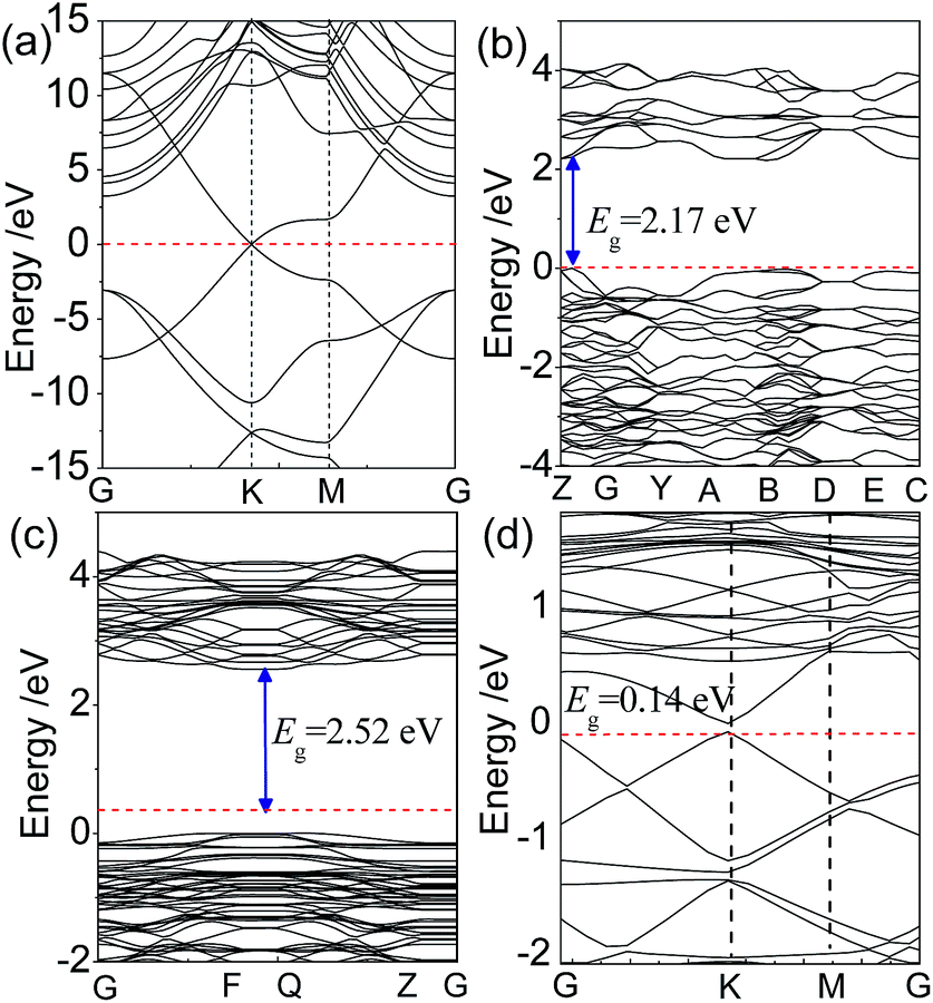 | ||
| Fig. 3 Calculated energy band structures of (a) graphene, (b) bulk BiVO4, (c) BiVO4(001) sheet, and (d) graphene/BiVO4(001) heterojunction within the GGA-PBE formalism. The Fermi level is set to be 0 eV, indicated by the red dashed line. | ||
For the graphene/BiVO4(001) interface, it is found that by comparing Fig. 3a and c, the energy band structures can almost be divided into two groups (from the BiVO4(001) layer or from graphene), due to the weak vdW force between interlayers. This phenomenon is similar to that previously reported by Du et al. for a g-C3N4/graphene heterobilayer,35 in which the energy bands near the Fermi level can almost be divided into two groups (from g-C3N4 or from graphene) as a result of the relatively weak interlayer coupling. It is noted that the typical conical structures of the π and π* bands of graphene in the vicinity of the Fermi level are split into double parts (two lines), which is different from those of the isolated graphene. In the graphene/BiVO4(001) interface with the equilibrium interlayer distance d = 2.99 Å, it can be seen that the π and π* linear dispersion bands separate from each other near the Fermi level at the K point, forming a small band gap of 0.14 eV, as shown in Fig. 3d. Thus, graphene adsorbed on the BiVO4(001) surface is no longer a metallic material with massless electrons, but a semiconductor with a direct narrow fundamental band gap. Unfortunately, for the BiVO4–graphene system, the band gap energy is difficult to estimate experimentally from the UV-vis diffuse reflectance spectra data.14
Furthermore, we calculated their density of states (DOS) and corresponding partial density of states (PDOS) with the equilibrium interlayer distance d = 2.99 Å between −15 eV and 10 eV, as shown in Fig. 4a. For BiVO4, the VB is composed of hybrid orbitals of Bi 6s and O 2p, whereas the CB is composed of V 3d orbitals.36 For the graphene/BiVO4(001) heterojunction, the new VB maximum and CB minimum are mainly contributed to by the pz orbital of the C atoms in the graphene layer. It is noted that the O 2p and V 3d states of the BiVO4(001) layer in the interface extend so that they are neighbouring the Fermi level from the two directions of the VB and CB. Thus, the hybridization between the BiVO4(001) surface and graphene results in a serious decrease of the band gap of BiVO4 in the interface. And the charge transfer is supposed to take place from Bi 6s and O 2p hybrid orbitals to V 3d orbitals upon photoexcitation. As a consequence of this, the introduced states neighbouring the Fermi level greatly enhance the carrier mobility, thus promoting the separation of photogenerated e−/h+ pairs.
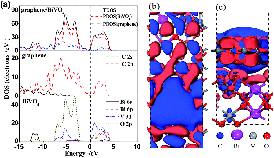 | ||
| Fig. 4 (a) Calculated total DOS of the graphene/BiVO4(001) heterojunction and PDOS of graphene and BiVO4(001) sheets within the GGA-PBE formalism. The vertical dashed line is the Fermi level. Top (b) and side (c) views of the charge density difference of the graphene/BiVO4(001) interface. Blue and red isosurfaces represent charge accumulation and depletion in the space with respect to isolated BiVO4 and graphene, respectively. The isovalue chosen to plot the isosurface is 0.001 e Å−3. | ||
To further investigate the charge transfer between the BiVO4(001) surface and graphene, the charge density difference was investigated and Milliken analysis was performed to reveal the interlayer charge transfer between graphene and BiVO4. The charge density difference, ρgraphene/BiVO4(001) = ρgraphene + ρBiVO4(001), can be obtained by subtracting the electronic charge of the graphene/BiVO4(001) interface from that of the corresponding isolated graphene and BiVO4(001) surfaces. Fig. 4b and c clearly show that the charge density is redistributed by forming electron-rich and hole-rich regions within the graphene/BiVO4(001) interface. Through Milliken analysis, there is an average charge transfer of 0.04|e| from every top Bi atom to graphene when graphene adsorbs on the BiVO4 (001) surface. In the meantime, the charge transfer of 0.02|e| happens from graphene to every top O atom. This fact implies that the inhomogeneous onsite energy between the interlayers is induced not only by the inhomogeneous charge redistribution between the interlayers caused by graphene, but also by the charge transfer between the BiVO4(001) surface and graphene. As a consequence, the hybridization between graphene and the BiVO4(001) surface disrupts the degeneracy of the π and π* bands of graphene at the K point, resulting in its semiconducting character.
Band edge potentials
To investigate the energy level match between the two components for charge transfer and separation in the heterostructured interface, the band edge energies of the CB and VB of BiVO4 were estimated from the absolute electronegativity of the atoms and the band gap as follows:37,38
 | (4) |
| EV = EC + Eg | (5) |
The work function of a material is a critical parameter commonly used as an intrinsic reference for band alignment. Here, the work function is calculated and the corresponding energy level lineup diagrams for BiVO4 and graphene before and after equilibrium are plotted, as shown in Fig. 5. The work function is defined as follows:40
| Φ = Evac − EF | (6) |
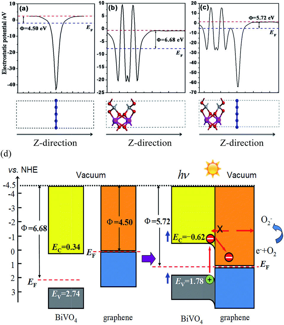 | ||
| Fig. 5 The electrostatic potentials for (a) graphene, (b) the BiVO4(001) sheet and (c) the graphene/BiVO4(001) heterojunction. The red and blue dashed lines represent the vacuum level, E0, and the Fermi level, EF, respectively. (d) Diagram of the band edge positions before and after contact of graphene and BiVO4. | ||
As an n-type photocatalyst, the good hole conductivity of BiVO4 is highly favorable for hole transfer, which is critical for both photocatalytic and photoanodic water oxidation.15,41 The Fermi level of BiVO4 is located under the CB and is slightly more positive than that of graphene. After equilibration of the graphene/BiVO4(001) interface, the Fermi levels shift in the negative direction for BiVO4 and the positive direction for graphene, respectively, until they are equal. At this time, the CB and VB of BiVO4 are pulled in the negative direction a little, and then form a slightly downward band bending close to the interface between BiVO4 and graphene. It is reasonable to say that under visible-light irradiation, the electrons receiving photon energy in the BiVO4 layer transit from the VB to the CB, then continuously flow into graphene via a percolation mechanism,42 through which the electrons in graphene cannot migrate back to BiVO4 and thus are trapped in graphene. The n-type-like Schottky junction thus boosts the flow of electrons from BiVO4 to graphene and leaves holes in BiVO4, facilitating the separation of photogenerated carriers.43 In effect, these electrons on the surface of graphene sheets can be captured easily by the adsorbed O2 molecules to produce superoxide radical anions, ˙O2−, because the standard redox potential of O2/˙O2− (−0.28 V vs. NHE) is more negative than the CB potential of graphene in the interface.44 In this case, the VB potential (1.77 V vs. NHE) of the BiVO4 layer is less positive than the standard redox potential of ˙OH/OH− (1.99 V vs. NHE), indicating that the photogenerated holes in the VB of the BiVO4 layer could not oxidize OH− into ˙OH free radicals with a very strong oxidation capacity. Of course, the VB edge is more positive than the redox potential of RhB (1.43 V).45 This ascertains, for example, that in the system, direct photogenerated hole oxidation is energetically possible and will photodegrade RhB.46,47 So the superoxide radical anions, ˙O2−, and photogenerated holes are responsible for the degradation of RhB.
Optical absorption
To examine the effect of graphene combination on the photocatalytic efficiency of BiVO4, the optical spectra were investigated by calculating the imaginary part of the complex dielectric function using the GGA-PBE method. It is well known that the allowed transitions are determined by the nonzero matrix elements of the position operator. Here, the optical calculations are achieved using plane polarization with the specified polarization direction where the E field vector is parallel to the x, y or z axes (marked as E∥x, E∥y, E∥z) and the “polycrystalline” polarization where the E field vector is an isotropic average over all directions. In the optical spectra analysis, a small smearing of 0.2 eV is used to greatly distinguish the absorption peaks.Fig. 6 shows the polycrystalline and polarized optical absorption coefficient spectra of the isolated BiVO4 layer and graphene/BiVO4 interface. For the isolated BiVO4 layer, in the polarization direction of E∥x and E∥y, it is noted that the optical properties are almost the same prominent peaks between 500 and 550 nm, while a different curve is obtained along the polarization direction of E∥z, as shown in Fig. 6c, which indicates that the BiVO4 layer has strong optical anisotropy. The similarity of the absorption coefficient spectra under E∥x and E∥y is certainly reasonable since the symmetry of the absorption coefficient spectra corresponds to the symmetry of the lattice structure in the plane directions. In fact, the previous results show clearly that the absorption edge of pure BiVO4, corresponding to the largest wavelength, is about 520 nm, which indicates that BiVO4 is a visible-light semiconductor photocatalyst.3,47 However, the absorption intensity of pure BiVO4 is so weak in the visible-light region that the optical absorption isn’t enough to contribute to the high photocatalytic activity of BiVO4.
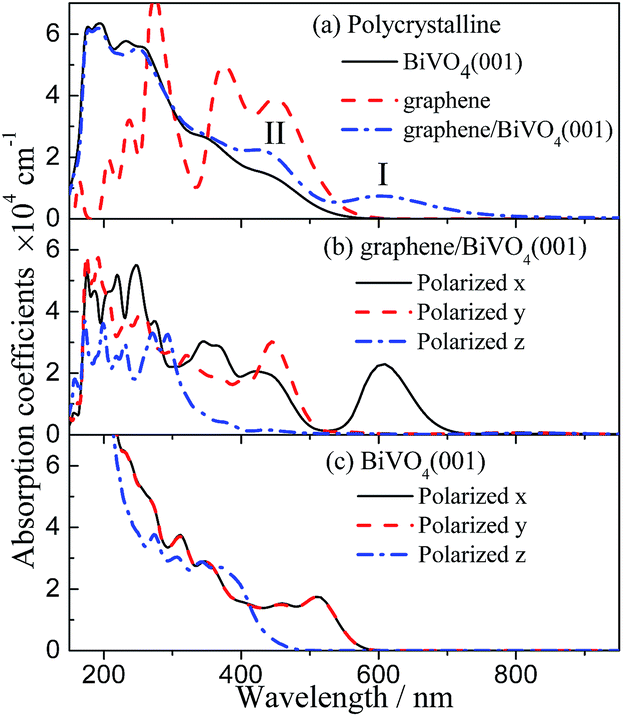 | ||
| Fig. 6 Calculated polycrystalline and polarized optical absorption coefficient spectra of the graphene/BiVO4 interface and BiVO4(001) sheet. | ||
It can be seen from the polycrystalline curve of the optical absorption coefficient spectra of the graphene/BiVO4(001) heterojunction in Fig. 6a that the absorption edges extend to more than 950 nm. In addition, Fig. 6b shows that the absorption coefficient spectra of the graphene/BiVO4(001) heterojunction have certain anisotropy in the long wavelength region. By analyzing Fig. 6b, it is found that the two prominent peaks (I and II) in Fig. 6a are mainly contributed to by the absorption coefficient spectra under E∥x and E∥y. It is noteworthy that peak I at 610 nm is mainly contributed to by the effect of the graphene layer on the BiVO4(001) surface, namely, the inhomogeneous charge redistribution between interlayers caused by graphene. Further, it is noted that the absorption coefficient spectrum under E∥x has much stronger signals than those under E∥y and E∥z in the visible-light region, which is attributed to a delocalized electron transition, and is not related to the crystal structure. It is inferred that peak II at 440 nm corresponds to a phototransition energy of about 2.82 eV, from the top of the VB to V 3d levels in the CB of the BiVO4 layer, or Bi 6s and O 2p levels in the VB of the BiVO4 layer to the bottom of the CB. Compared with the results for pure BiVO4, the absorption intensity of the graphene/BiVO4(001) heterojunction increases a lot in the visible-light region due to the large distribution of C 2p states near the new bottom of the CB and the new top of the VB. In fact, Fu et al. also reported that the UV-vis diffuse reflectance spectra of pure BiVO4 and BiVO4–graphene photocatalysts show that there is no significant absorption in the region of 520–850 nm for pure BiVO4, while the absorption of BiVO4–graphene is much stronger than that of pure BiVO4 particles covering the whole visible-light region due to the presence of graphene.14 It is reasonable to consider that the hybridization between BiVO4 layers and graphene induces an increase in the optical absorption range and intensity of BiVO4 in the visible-light region,14,23,47 and thus their visible-light absorption is enough to contribute to the high photocatalytic activity of heterostructured systems.
Conclusions
The microscopic mechanisms of interface interactions, charge transfer and separation, as well as their influence on the photocatalytic activity of graphene/BiVO4(001) heterojunctions have been studied by first-principles calculations incorporating semiempirical dispersion-correction schemes to correctly describe vdW interactions. The mismatch of initial lattice parameters between the optimized graphene and BiVO4(001) layers is only 1.6–1.8%, and the results indicate that the BiVO4(001) surface and graphene are in contact and form a vdW heterostructured interface. By analyzing the energy level based on our calculated work function between the two components, it can be found after equilibration of the graphene/BiVO4(001) interface that the electrons receiving photon energy in the BiVO4(001) layer continuously flow into the C pz orbital of graphene under visible-light irradiation, in which the electrons cannot migrate back to BiVO4 and thus are trapped in graphene, facilitating the separation of photogenerated carriers. It is further indicated that the hybridization between the two components induces an increase of optical absorption of BiVO4 in the visible-light region. In short, the incorporation of graphene into BiVO4 facilitates the separation of photogenerated e−/h+ pairs and the enhancement of visible-light absorption. The present investigation is useful in the wider development of new BiVO4-based heterojunction photocatalysts.Acknowledgements
This work was supported by the National Natural Science Foundation of China (No. 51472081, 21301135, 51202064), the Foundation for High-Level Talents (GCRC13014), and the Development Funds of Hubei Collaborative Innovation Center (HBSKFMS2014003, HBSKFMS2014011, HBSKFMS2015004).Notes and references
- A. Kudo, K. Omori and H. Kato, J. Am. Chem. Soc., 1999, 121, 11459–11467 CrossRef CAS.
- K. Shantha and K. B. R. Varma, Mater. Sci. Eng., B, 1999, 60, 66–75 CrossRef.
- S. Tokunaga, H. Kato and A. Kudo, Chem. Mater., 2001, 13, 4624–4628 CrossRef CAS.
- L. Zhang, D. Chen and X. Jiao, J. Phys. Chem. B, 2006, 110, 2668–2673 CrossRef CAS PubMed.
- D. Wang, R. Li, J. Zhu, J. Shi, J. Han, X. Zong and C. Li, J. Phys. Chem. C, 2012, 116, 5082–5089 CAS.
- X. Zhang, Z. Ai, F. Jia, L. Zhang, X. Fan and Z. Zou, Mater. Chem. Phys., 2007, 103, 162–167 CrossRef CAS.
- T. W. Kim and K.-S. Choi, Science, 2014, 343, 990–994 CrossRef CAS PubMed.
- Y. Sun, Y. Xie, C. Wu, S. Zhang and S. Jiang, Nano Res., 2010, 3, 620–631 CrossRef CAS.
- G. Xi and J. Ye, Chem. Commun., 2010, 46, 1893–1895 RSC.
- M. Guo, Y. Wang, Q. L. He, W. J. Wang, W. M. Wang, Z. Y. Fu and H. Wang, RSC Adv., 2015, 5, 58633–58639 RSC.
- D. K. Zhong, S. Choi and D. R. Gamelin, J. Am. Chem. Soc., 2011, 133, 18370–18377 CrossRef CAS PubMed.
- S. J. Hong, S. Lee, J. S. Jang and J. S. Lee, Energy Environ. Sci., 2011, 4, 1781–1787 CAS.
- M. Long, W. Cai, J. Cai, B. Zhou, X. Chai and Y. Wu, J. Phys. Chem. B, 2006, 110, 20211–20216 CrossRef CAS PubMed.
- Y. Fu, X. Sun and X. Wang, Mater. Chem. Phys., 2011, 131, 325–330 CrossRef CAS.
- Y. Park, K. J. McDonald and K.-S. Choi, Chem. Soc. Rev., 2013, 42, 2321–2337 RSC.
- J. H. Kim and J. S. Lee, Energy and Environment Focus, 2014, 3, 339–353 CrossRef.
- J. Jiang, X. Zhang, P. B. Sun and L. Z. Zhang, J. Phys. Chem. C, 2011, 115, 20555–20564 CAS.
- S. C. Yan, S. B. Lv, Z. S. Li and Z. G. Zou, Dalton Trans., 2010, 39, 1488–1491 RSC.
- L. Ge, C. C. Han and J. Liu, Appl. Catal., B, 2011, 100, 108–109 Search PubMed.
- Z. Liu, Q. Liu, Y. Huang, Y. Ma, S. Yin, X. Zhang, W. Sun and Y. Chen, Adv. Mater., 2008, 20, 3924–3930 CrossRef CAS.
- D. Wang, D. Choi, J. Li, Z. Yang, Z. Nie, R. Kou, D. Hu, C. Wang, L. V. Saraf, J. Zhang, I. A. Aksay and J. Liu, ACS Nano, 2009, 3, 907–914 CrossRef CAS PubMed.
- Q. J. Xiang, J. G. Yu and M. Jaroniec, Chem. Soc. Rev., 2012, 41, 782–796 RSC.
- Y. Sun, B. Qu, Q. Liu, S. Gao, Z. Yan, W. Yan, B. Pan, S. Wei and Y. Xie, Nanoscale, 2012, 4, 3761–3767 RSC.
- D. Wang, H. Jiang, X. Zong, Q. Xu, Y. Ma, G. Li and C. Li, Chem.–Eur. J., 2011, 17, 1275–1282 CrossRef CAS PubMed.
- R. Munprom, P. A. Salvador and G. S. Rohrer, J. Mater. Chem. A, 2015, 3, 2370–2377 CAS.
- J. P. Perdew, K. Burke and M. Ernzerhof, Phys. Rev. Lett., 1996, 77, 3865–3868 CrossRef CAS PubMed.
- D. M. Ceperley and B. J. Alder, Phys. Rev. Lett., 1980, 45, 566–569 CrossRef CAS.
- S. Grimme, J. Comput. Chem., 2006, 27, 1787–1799 CrossRef CAS PubMed.
- F. Ortmann, F. Bechstedt and W. G. Schmidt, Phys. Rev. B: Condens. Matter Mater. Phys., 2006, 73, 205101–205110 CrossRef.
- H. J. Monkhorst and J. D. Pack, Phys. Rev. B: Solid State, 1976, 13, 5188–5192 CrossRef.
- A. W. Sleight, H. Chen, Y. A. Ferretti and D. E. Cox, Mater. Res. Bull., 1979, 14, 1571–1581 CrossRef CAS.
- J. Zhang, F. Ren, M. Deng and Y. Wang, Phys. Chem. Chem. Phys., 2015, 17, 10218–10226 RSC.
- Y. D. Ma, Y. Dai, W. Wei, C. W. Niu, L. Yu and B. B. Huang, J. Phys. Chem. C, 2011, 115, 20237–20241 CAS.
- Y. D. Ma, Y. Dai, M. Guo and B. B. Huang, Phys. Rev. B, 2012, 85, 235448–235455 CrossRef.
- A. J. Du, S. Sanvito, Z. Li, D. W. Wang, Y. Jiao, T. Liao, Q. Sun, Y. H. Ng, Z. H. Zhu, R. Amal and S. C. Smith, J. Am. Chem. Soc., 2012, 134, 4393–4397 CrossRef CAS PubMed.
- M. Oshikiri, M. Boero, J. Ye, Z. Zou and G. Kido, J. Chem. Phys., 2002, 117, 7313–7318 CrossRef CAS.
- Y. Xu and M. A. A. Schoonen, Am. Mineral., 2000, 85, 543–556 CrossRef CAS.
- W. J. Chun, A. Ishikawa, H. Fujisawa, T. Takata, J. N. Kondo, M. Hara, M. Kawai, Y. Matsumoto and K. Domen, J. Phys. Chem. B, 2003, 107, 1798–1803 CrossRef CAS.
- H. Jiang, H. Endo, H. Natori, M. Nagai and K. Kobayashi, J. Eur. Ceram. Soc., 2008, 28, 2955–2962 CrossRef CAS.
- R. Garg, N. K. Dutta and N. R. Choudhury, Nanomaterials, 2014, 4, 267–300 CrossRef.
- Z. Li, W. Luo, M. Zhang, J. Feng and Z. Zou, Energy Environ. Sci., 2013, 6, 347–370 CAS.
- X. Wang, L. J. Zhi and K. Müllen, Nano Lett., 2008, 8, 323–327 CrossRef CAS PubMed.
- Y. H. Ng, A. Iwase, A. Kudo and R. Amal, J. Phys. Chem. Lett., 2010, 1, 2607–2612 CrossRef CAS.
- T. Berger, D. Monllor-Satoca, M. Jankulovska, T. Lana-Villarreal and R. Gomez, ChemPhysChem, 2012, 13, 2824–2875 CrossRef CAS PubMed.
- T. Shen, Z. G. Zhao, Q. Yu and H. J. Xu, J. Photochem. Photobiol., A, 1989, 47, 203–212 CrossRef CAS.
- S. B. Gawande and S. R. Thakare, Int. Nano Lett., 2012, 2, 11–17 CrossRef.
- Y. Li, Z. Sun, S. Zhu, Y. Liao, Z. Chen and D. Zhang, Carbon, 2015, 94, 599–606 CrossRef CAS.
| This journal is © The Royal Society of Chemistry 2017 |