DOI:
10.1039/C6RA25704F
(Paper)
RSC Adv., 2017,
7, 4806-4814
Proposition and computational analysis of a kesterite/kesterite tandem solar cell with enhanced efficiency
Received
23rd October 2016
, Accepted 2nd January 2017
First published on 17th January 2017
Abstract
We propose a dual junction Cu2ZnSnS4/Cu2ZnSnSe4 (kesterite/kesterite) based tandem configuration and analyze its prospect and viability as a solar cell. Cu2ZnSnS4 and Cu2ZnSnSe4, both having the kesterite crystal structure, are used as the main absorbers for the top and bottom of cells, respectively. We optimize the thickness of the absorbers using optoelectronic simulations and investigate the effect of absorber thickness on short circuit current density and open circuit voltage. The optimized thicknesses for peak efficiency are found to be 200 nm and 850 nm for Cu2ZnSnS4 and Cu2ZnSnSe4, respectively. The maximum efficiency of the tandem cell is estimated to be 19.87% including recombination effects such as Shockley–Read–Hall (SRH) and radiative recombination mechanisms. We also investigate the effect of band gap on the performance of the tandem cell and show that a 21.74% efficient tandem cell can be achieved for optimized band gaps. Finally, we report that efficiency could be further enhanced by replacing the CdS buffer layer with eco-friendly ZnS buffer layer and optimizing the tandem structure. The proposition and computational analysis presented in this work may help in achieving higher efficiency kesterite solar cells.
Introduction
In order to avoid negative irreversible effects of traditional energy resources (such as fossil fuels or nuclear power plants etc.), energy harvesting through solar photovoltaics is on the leading edge among other renewable energy resources. Although silicon based solar cells currently share about 85% of the total photovoltaic market,1 chalcogenide-based thin film solar cells (such as CIGS, CdTe, CZTS etc.) are being explored extensively among other promising structures and may form the foundation of next generation photovoltaics technology because of their high power conversion efficiency (PCE), low material usage, direct and tunable band gap and low deposition cost on a large area.1–5 Despite the fact that CuIn1−xGaxSe2 (CIGS) based solar cells hold the world record efficiency value (21.7%)6 among all thin film technologies, the usage of earth rarer costly metals (e.g. indium (In), gallium (Ga)) makes their production limited. Kesterite photovoltaics, utilizing Cu2ZnSnS4 (CZTS), Cu2ZnSnSe4 (CZTSe) and Cu2ZnSn(S1−xSex)4 (CZTSSe) absorbers, are emerging as one of the most promising replacement for the chalcopyrite solar cells through the substitution of the rarer metals In and Ga of the CIGS absorber with comparatively earth-abundant and lower cost zinc (Zn) and tin (Sn).6–9 In addition, kesterite absorbers exhibit high absorption coefficient (>104 cm−1) and direct tunable band gap in the range of 1.0–1.56 eV which allow effective absorption of incident photons in few microns' thickness of absorbers.10–12 Moreover, their properties are closely related to CIGS absorbers because of the similarity in crystal structure and isovalency.1,7,13–15 All these facts make kesterite an interesting field of research. However, kesterite solar cell currently suffers from open circuit voltage deficit and poor efficiency. The highest efficiency reported by single junction kesterite solar cell is 12.6% employing CZTSSe absorber with an open circuit of 510 mV.6,11 The limiting factors behind poor performance are bulk defects, secondary phase formation, grain boundaries, kesterite/buffer layer and kesterite/back contact interfaces.10,12,16 Therefore, in order to compete with existing solar cell technologies, significant research and effort are needed.
Recently, Hsieh et al. reported efficiency enhancement through K-doping and optimization of n-type window layer.17 However, rear surface recombination and poor minority carrier life time in kesterite absorbers significantly reduce the fill factor of their reported cell. Another attempt was made by Neuschitzer et al. by manipulating grain growth with Ge doping.18 However, shallow defects were identified in the cell for optimal and high Ge doping which act as electron–hole recombination centers and limit the photovoltaic efficiency significantly. Kim et al. enhanced carrier life time by controlling the thickness of ZnS precursor layer which increased the PCE of single junction kesterite solar cell up to 9.1% with CZTSSe absorber.19 It was also reported that the performance can be further improved with Al2O3 rear surface passivation layer with nanosized point openings by reducing rear surface recombination and the impact of secondary phase segregation.20 Further, interfacial microstructure and chemistry of CdS/CZTS heterojunction were studied by Liu et al.21 They improved the minority carrier life time by eliminating interfacial defects with chemical bath deposition (CBD) process. However, the disposal and waste recycling process in CBD could be a matter of concern for industry.22 Different types of hybrid buffer layer were also used to increase open circuit voltage and efficiency of kesterite solar cell.23,24 Although noteworthy increases in PCE of kesterite solar cell have been achieved in recent years, further improvements are still required to enhance efficiency up to the level of CIGS solar cells and to increase the commercial viability of these types of photovoltaics.
In order to increase the open circuit voltage and enhance the efficiency, tandem junction topology is an established technique. Recently, Todorov et al. reported perovskite/CZTSSe solar cell with an efficiency of 16%.25 The performance of their perovskite/CZTSSe cell is limited by high resistance and low optical transmission of aluminum (Al) layer. The cell suffers from stability issues due to perovskite26 and increased fabrication cost due to high annealing temperature.27 Moreover, other disadvantages of perovskites such as limited device life time, poor crystallinity, degradation under environmental influence,28 use of toxic metal (lead),29 uncontrollable surface morphology30 etc., the use of perovskite/CZTSSe need more organized research on perovskites. Although, kesterite absorbers are suitable for both upper and lower cells in multi-junction solar cells due to their tunable band gap property, no kesterite/kesterite tandem cell has yet been reported in literature. Such tandem junction solar cell would be eco-friendly having low fabrication cost as well as printable with existing technologies.31–34 Moreover, this may overcome the limitations of perovskite/CZTSSe cell with the use of CZTS in place of perovskite. In this work, we investigate the prospect of kesterite/kesterite dual-junction tandem solar cells by computational analysis where CZTS (band gap ∼ 1.56 eV)35 and CZTSe (band gap ∼ 1.04 eV)36 are used as absorber layers for top and bottom cells, respectively. We optimize the structure to achieve maximum efficiency out of these structures. We also analyze the effect of top and bottom cells' band gap and composition of buffer layer on the efficiency of our proposed tandem cell.
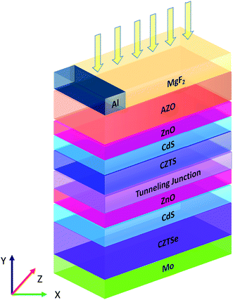
Simulation methodology
Fig. 1 represents the structure of a CZTS/CZTSe tandem junction solar cell. CZTS and CZTSe are the main absorbing materials of top and bottom cells, respectively. We have designed the top cell architecture according to the experimental structure reported by Shin et al.37 The cell layers are AZO/ZnO/CdS/CZTS. Here, CdS is utilized as a buffer layer and n-doped transparent ZnO window layer works as the top surface field layer. Aluminum doped ZnO (AZO) is used to reduce the series resistance of the overall tandem cell. The thicknesses of AZO, ZnO and CdS in the top cell are 400 nm, 50 nm and 70 nm, respectively. A 100 nm thick magnesium fluoride (MgF2) is placed on top as an antireflection coating layer. On the other hand, we have followed the experimental design proposed by Wang et al.11 to model the bottom cell structure. The bottom cell consists of ZnO/CdS/CZTSe. The roles of CdS and ZnO are similar to that of the top cell. The thicknesses of ZnO, CdS and Mo in the bottom cell are 50 nm, 150 nm and 500 nm, respectively. As shown in Fig. 1. Molybdenum (Mo) is used as the back contact whereas Al contact with 10% coverage is used as the front electrode. A tunneling junction made of ITO is considered between the two cells. Such tunneling junction with ITO has been experimentally fabricated by Todorov et al.25 Also, CZTS/ITO and ITO/ZnO interfaces have been shown to be experimentally realizable.38–41 Therefore, the proposed tandem structure can be implemented with the existing fabrication technology.
 |
| | Fig. 1 The structure of Cu2ZnSnS4/Cu2ZnSnSe4 tandem cell. | |
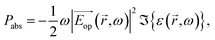
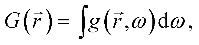
Study of the structure shown in Fig. 1 was done in two parts: (a) calculation of absorption and carrier generation through optical simulation and (b) estimation of PCE from electrical simulation. In the optical part, we solved Maxwell's curl equations through finite difference time domain (FDTD) analysis to find out the optical electric field  distribution inside different layers. Each material was modeled by its respective refractive index (n) and extinction coefficient (κ) as a function of wavelength. Then, the absorbed power (Pabs) can be calculated from optical electric field distribution and imaginary part of complex dielectric constant as
| |
 | (1) |
where
ω is the angular frequency and
ε(
![[r with combining right harpoon above (vector)]](https://www.rsc.org/images/entities/i_char_0072_20d1.gif)
,
ω) is the dielectric constant. The generation rate,
G(
) was calculated according to the following equations:
| |
 | (2) |
| |
 | (3) |
where
h is the Planck's constant. Periodic boundary condition was used in horizontal (
X) direction and perfectly matched layer (PML) boundary condition was applied for top and bottom faces (in
Y-direction). AM 1.5G standard solar spectrum has been used as the input radiation source.
The electrical characteristics were calculated in two steps. In the first step, we simulated top and bottom cells separately and calculated their characteristics features. In this regard, we solved the Poisson's equation, drift–diffusion equations and continuity equations (eqn (4)–(8)) self consistently for electrons and holes and find the J–V characteristics, open circuit voltage (Voc), short circuit current (Jsc), fill factor (FF) and efficiency (η) of top and bottom cells independently.
| |
 | (5) |
| |
 | (6) |
| |
 | (7) |
| |
 | (8) |
where
εdc is the dc dielectric permittivity,
V is the electrostatic potential (electric field,
![[E with combining right harpoon above (vector)]](https://www.rsc.org/images/entities/i_char_0045_20d1.gif)
= −∇
V),
ρ is the net charge density (
ρ =
p −
n +
C, which includes the contribution
C from the ionized impurity density),

is the electron (hole) current density,
q is the positive electron charge,
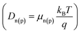
μn(p) is the mobility of electron (hole),
Dn(p) is the diffusivity of electron (hole)
,
n and
p are electron and hole densities, respectively,
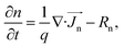
Rn(p) is the net recombination rate (the difference between the recombination rate and generation rate),
kB is the Boltzmann constant and
T is the temperature (the subscripts n and p indicate quantities that are specific to the carrier type). Generation rate calculated from the optical simulation was given as an input in the continuity equations and the equation set (
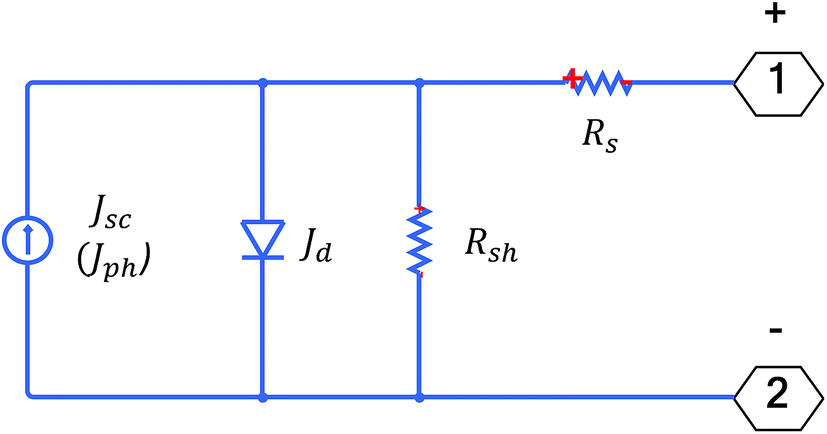
eqn (4)–(8)) were solved self-consistently. In this way, we found the individual characteristics of top and bottom cells. We have used Lumerical FDTD and Device solvers for the optical and electrical simulations, respectively. The cells were modeled by the equivalent circuit shown in
Fig. 2. In the circuit,
Jph is the photon generated current density,
Rs and
Rsh represent series and shunt resistances, respectively. The current density through the diode,
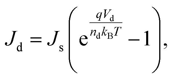
Jd can be calculated from:
| |
 | (9) |
where
Js is the dark diode reverse-saturation current,
Vd is the bias voltage across the diode and
nd is the ideality factor.
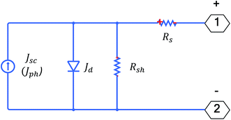 |
| | Fig. 2 Equivalent circuit for individual cells. | |
Once we obtained the model parameters of each cell, we applied the series circuit rules on top and bottom cells' parameters via Matlab simulink and generated the J–V characteristics of the tandem cell (Fig. 3). The tunneling junction was modeled as ohmic contact. One of the main advantages of using this approach is that a comparison can be conveniently made with the performance of individual cells as well as their roles in the tandem configuration could be clearly comprehended. Using circuit model for computing tandem cell characteristics is also computationally efficient.
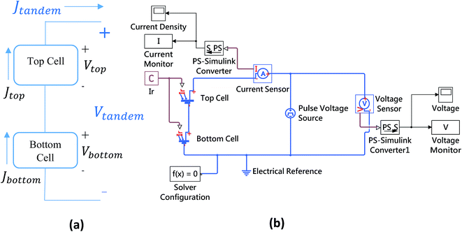 |
| | Fig. 3 (a) Topology of Cu2ZnSnS4/Cu2ZnSnSe4 tandem stacks (b) circuit diagram of simulated overall tandem structure. | |
Results and discussion
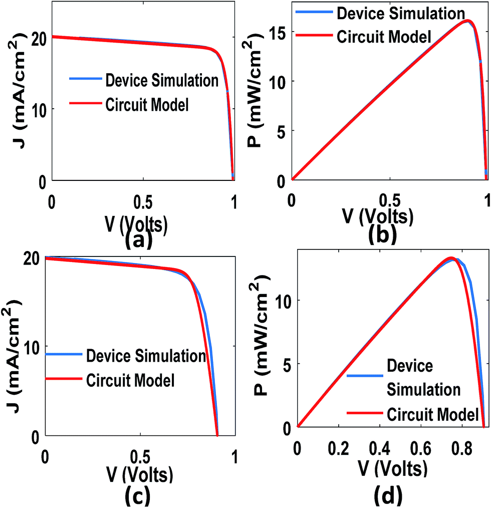
At first, we benchmarked the J–V characteristics derived from circuit model with the device simulation results for each cell. To match these characteristics, we first assumed that equivalent circuit only comprised of a photon generated current source (Jph), a diode (Jd) and a shunt resistance (RSh). Then, we simulated the J–V characteristics from device simulation without considering recombination and compared these characteristics with the circuit model. In the next step, we calculated J–V characteristics from device simulation considering recombination parameters and matched the same with circuit model considering series resistance (Rs) in the model. In order to get the best possible match, we considered that ideality factor (nd) is 1.01 and 1.015 for top and bottom cells, respectively. Jph is assumed to be equal to Jsc and Js is calculated from Voc. Series resistances for both top and bottom cells are low enough to validate the assumption Jph = Jsc. The values of Rs and RSh are dynamically changed with absorber thickness to match the J–V characteristics of device simulation. Typical matching of J–V and P–V characteristics for 230 nm CZTS and 850 nm CZTSe absorbers is shown for top and bottom cells in Fig. 4 and 5, respectively. Also, Table 1 shows a comparison of Voc, Jsc, FF and η of the circuit model with device simulations.
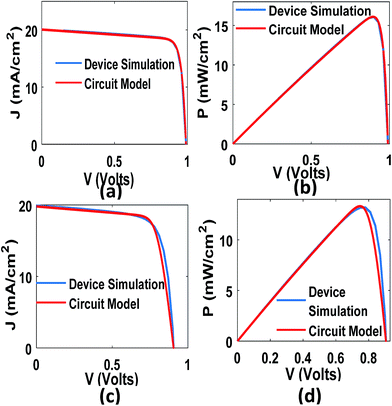 |
| | Fig. 4 Comparison between device simulation and circuit model for top cell (a) J–V characteristic without recombination (b) P–V characteristic without recombination, (c) J–V characteristic with recombination and (d) P–V characteristic with recombination. | |
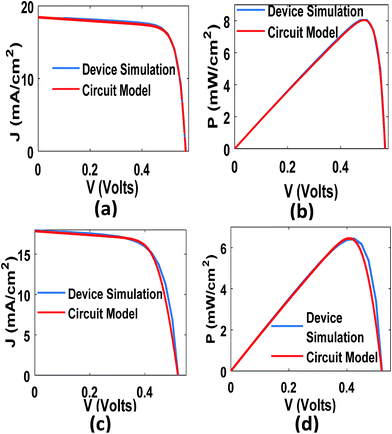 |
| | Fig. 5 Comparison between device simulation and circuit model for bottom cell (a) J–V characteristic without recombination (b) P–V characteristic without recombination, (c) J–V characteristic with recombination and (d) P–V characteristic with recombination. | |
Table 1 Comparison of performance metrics between device simulation and circuit model
| |
|
|
Voc (V) |
Jsc (mA cm−2) |
FF |
Efficiency (%) |
| Without recombination |
Top cell (CZTS) |
Device simulation |
0.990 |
20.06 |
0.810 |
16.09 |
| Circuit model |
0.990 |
20.06 |
0.811 |
16.10 |
| Bottom cell (CZTSe) |
Device simulation |
0.569 |
18.43 |
0.768 |
8.05 |
| Circuit model |
0.568 |
18.43 |
0.767 |
8.04 |
| With recombination |
Top cell (CZTS) |
Device simulation |
0.906 |
19.93 |
0.731 |
13.20 |
| Circuit model |
0.905 |
19.79 |
0.744 |
13.32 |
| Bottom cell (CZTSe) |
Device simulation |
0.521 |
17.96 |
0.687 |
6.43 |
| Circuit model |
0.520 |
17.85 |
0.695 |
6.45 |
As can be seen from Table 1, circuit model is capable of reproducing the behavior of a cell under different conditions (with or without considering recombination). Thus, we modeled the experimental structures to benchmark our used parameters. Table 2 shows the comparison of our model with experimentally reported values. In this regard, the optical and basic electrical parameters as well as recombination parameters were taken from literature (optical,15,42–50 electrical15,36,51–61 (listed in Table 3)). We considered SRH recombination mechanism for bulk defect and radiative recombination mechanisms for the direct band gap nature of the absorbers. We used much less carrier life time than that of the reported values in literature to predict the minimum performance limit of the proposed tandem structure.
Table 2 Comparison of simulation results with the experimental data of individual cells
| |
Voc (V) |
Jsc (mA cm−2) |
FF |
Efficiency (%) |
| Top cell |
| Experimental37 |
0.661 |
19.50 |
0.658 |
8.40 |
| Simulation |
0.648 |
21.25 |
0.621 |
8.54 |
![[thin space (1/6-em)]](https://www.rsc.org/images/entities/char_2009.gif) |
| Bottom cell |
| Experimental11 |
0.513 |
35.20 |
0.698 |
12.60 |
| Simulation |
0.533 |
33.91 |
0.704 |
12.73 |
Table 3 Basic electrical parameters and recombination parameters used in simulations
| Features |
CZTS (p)15,56,57 |
CZTSe (p)15,36,51 |
CdS (n)58,59 |
ZnS (n)52,55,58,59 |
ZnO (n+)53,54,58–60 |
AZO (n++)58,59,61 |
| DC permittivity |
7 |
7 |
10 |
9 |
9 |
9 |
| Band gap (eV) |
1.56 |
1.04 |
2.42 |
3.58 |
3.37 |
3.37 |
| Electron affinity (eV) |
4.1 |
4.05 |
3.75 |
3.8 |
4 |
4 |
| Electron effective mass (me/mo) |
0.18 |
0.07 |
0.25 |
0.22 |
0.275 |
0.275 |
| Hole effective mass (mp/mo) |
2 |
0.2 |
5 |
1.76 |
0.59 |
0.59 |
| Electron mobility (cm2 V−1 s−1) |
100 |
145 |
160 |
230 |
150 |
50 |
| Hole mobility (cm2 V−1 s−1) |
25 |
35 |
15 |
40 |
50 |
5 |
| Acceptor concentration (cm−3) |
5 × 10¹⁶ |
5 × 10¹⁵ |
0 |
0 |
0 |
0 |
| Donor concentration (cm−3) |
0 |
0 |
9 × 10¹⁶ (top) |
9 × 10¹⁶ (top) |
1.5 × 10¹⁷ |
8 × 10¹⁸ |
| 5 × 10¹⁶ (bottom) |
5 × 10¹⁶ (bottom) |
| SRH (life time in seconds) |
2.7 × 10⁻¹⁰ |
1.5 × 10⁻⁹ |
7.5 × 10⁻¹⁰ |
5.5 × 10⁻¹⁰ |
— |
— |
| Radiative recombination (ehp capture rate cm3 s−1) |
1.04 × 10⁻¹⁰ |
1.04 × 10⁻¹⁰ |
1.02 × 10⁻¹⁰ |
1.5 × 10⁻¹⁰ |
— |
— |
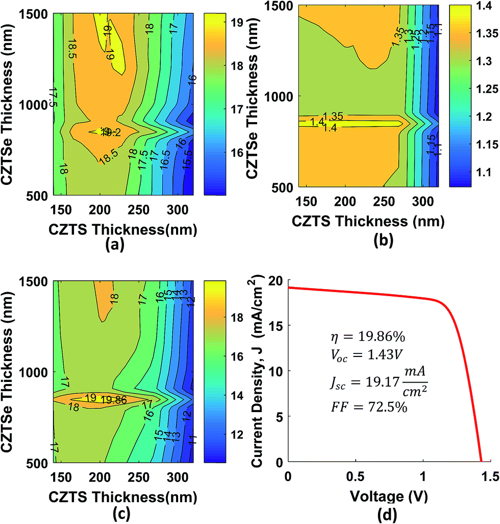
Having been convinced by the accuracy of our methodology, we analyzed and optimized the performance of the proposed CZTS/CZTSe tandem cell. To start the calculation with reasonable values of absorber thicknesses, we first examined the variation of PCE of top and bottom cells separately as a function of absorber thickness (Fig. 6). As can be seen from the figure, efficiencies of the top and bottom cells are maximized at ∼800 nm and ∼1200 nm thicknesses of CZTS and CZTSe, respectively. Therefore, as a starting point of our analysis, we chose a 600 nm thick CZTS and 1200 nm thick CZTSe absorbers keeping in mind the advantages of using thin films (note that we have later varied both absorber thicknesses within a wider range to arrive at an optimum combination). This yields an 8.89% efficient tandem cell with Voc = 1.124 V, Jsc = 11.98 mA cm−2 and FF = 0.679. In this configuration, efficiencies of the top and bottom cells are calculated to be 14.57% and 2.82%, respectively. Therefore, the tandem cell actually produces a lower efficiency than that of the top cell. The primary reason behind such poor performance of the tandem configuration can be attributed to the mismatch of current densities in top and bottom cells (Jsc,top = 23.24 mA cm−2, Jsc,bottom = 11.05 mA cm−2, Voc,top = 0.693 V, Voc,bottom = 0.451 V). Furthermore, the extra amount of current lost due to Jsc mismatching (as the tandem cell follows the cell with lower Jsc) may cause resistive heating which could further degrade the performance of tandem cell by lowering the band gap of the main absorbers.15 To avoid these unwanted effects and maximize the efficiency of tandem cell, current matching between top and bottom cells is the most crucial factor similar to any tandem configuration. Therefore, we attempted to match the short current density in top and bottom cells by varying the thickness of main absorbers. The results are summarized in Fig. 7.
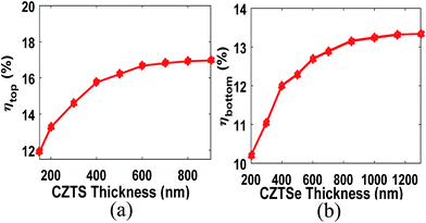 |
| | Fig. 6 Dependence of efficiencies of the top and bottom cells on the thickness of CZTS and CZTSe, respectively (a) top cell ηtop and (b) bottom cell ηbottom. | |
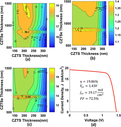 |
| | Fig. 7 Characteristics of tandem cell with the variation of the thickness of the main absorbers (a) short circuit current density Jsc, (b) open circuit voltage, Voc (c) efficiency, ηtandem and (d) J–V characteristics of optimized tandem cell where the thickness of CZTS and CZTSe are 200 nm and 850 nm, respectively. | |
Fig. 7(a) represents the dependence of tandem cell's Jsc on the thickness of CZTS and CZTSe absorbers. It is known that Jsc of the tandem cell is approximately equal to the minimum Jsc of top and bottom cells, and it maximizes when Jsc of top and bottom cells equals to each other. In tandem configuration, top and bottom cells absorb the shorter and longer wavelength photons of the solar spectrum, respectively. To match the Jsc of both cells, optical power absorption in two cells must be approximately equal. As the absorption depth of shorter wavelength photons is lower than that of longer wavelength photons, top cell absorbs a significant amount of radiation at a relatively lower thickness of the absorber (∼160 to 240 nm) which yielded a higher Jsc than that of the bottom cell as discussed above. To be equal with the top cell's Jsc, thickness of bottom cell's absorber must be increased. Loops in the Fig. 7(a) indicate higher Jsc regions where top and bottom cell's Jsc matches approximately. A maximum Jsc of 19.17 mA cm−2 was calculated in the tandem cell with ∼200 nm CZTS and ∼850 nm CZTSe. If the thickness of CZTS absorber is increased beyond 240 nm, it utilizes the solar spectrum in such a way that leaves small power behind for the bottom cell. In that case, Jsc of the bottom cell increases monotonically with the thickness of CZTSe absorber and fails to match with the Jsc of top cell. Since we observe high Jsc of tandem cell at multiple combinations of absorbers thickness, it is necessary to analyze the effect absorbers thickness on tandem cell's open circuit voltage, Voc.
We investigated the dependence of Voc on the absorber thicknesses and obtained a similar contour plot as shown in Fig. 7(b). The Voc of tandem cell is approximately equal to the summation of individual Voc of top and bottom cells, as expected. To maximize Voc of the tandem cell, individual open circuit voltages need to be maximized. In theory, Voc of a solar cell increases logarithmically with optical generation rate. However, recombination of electrons and holes significantly limits the increment of Voc at higher thicknesses. It can be seen that Voc of tandem cell remains high in the region of ∼140–260 nm CZTS and ∼850 nm CZTSe. Beyond that particular region, Voc of tandem cell falls due to recombination effects and mismatch of optical power absorption between top and bottom cells.
Finally, we analyzed the variation of tandem efficiency (ηtandem) with top and bottom cells' absorber thicknesses. We found that a maximum efficiency of 19.87% can be obtained for a particular combination of thicknesses (∼200 nm CZTS and ∼850 nm CZTSe). Fig. 7(d) shows the J–V characteristics of tandem cell at that particular combination while Fig. 8 shows the absorption spectrum for the same. We also calculated the efficiency of optimized tandem cell without recombination effects. That yields to a 23.94% efficient CZTS/CZTSe tandem cell with Voc = 1.542 V, Jsc = 19.83 mA cm−2 and FF = 0.785. Therefore, it can be inferred that low minority carrier life time significantly limits the efficiency of the CZTS/CZTSe solar cell by decreasing its open circuit voltage and fill factor significantly. It can also be noted that the proposed cell could yield 25% more efficiency (>20% as opposed to 16%) than that of perovskite/CZTSSe structure reported by Todorova et al.25
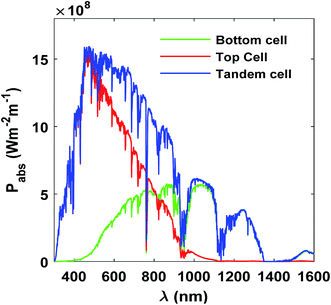 |
| | Fig. 8 Absorbed power spectrum (Pabs) of top and bottom cells along with the absorbed power of the tandem cell at different wavelengths (λ). | |
The experimentally reported tunable band gaps of CZTS and CZTSe vary in the range of 1.4–1.56 eV and, 0.9–1.12 eV (ref. 15, 35 and 36) respectively which enabled the proposed tandem configuration and thus far, we have used 1.56 eV and 1.04 eV as the band gap of CZTS and CZTSe, in that order. Now, we examine the dependence of tandem cell's Voc, Jsc and η on the band gap of main absorbers (Fig. 9), keeping the absorber thicknesses fixed at previously optimized values. Due to heterojunction characteristics, built-in potential of top and bottom cells increases with the band gap of absorbers.62 This increment results in overall increase in the built-in potential of the tandem cell. As a result, Voc of tandem cell is enhanced and a maximum value of 1.544 V was estimated (Fig. 9(a)). Moreover, the collection probability of electrons and holes in a solar cell increases with built-in potential which consequently increases its Jsc. As can be seen from Fig. 9(b), Jsc of tandem cell slightly increases with the band gap of CZTS and CZTSe. However, the increase in Jsc is relatively very small compared to the increase of Voc (7.69% (Voc) as opposed to 1.83% (Jsc)). Finally, Fig. 9(c) shows the variation of efficiency with the band gap of the absorbers. A maximum value of 21.74% was estimated when band gap of CZTS and CZTSe absorbers are both at their maximum values. It should be mentioned that kesterite being a fairly new field in the solar cell arena, detail and concrete material data as well as analysis are still not available for all compositions (for example, variation of optical constants with band gaps). Thus, in this band gap dependency analysis, we have used the same refractive index and extinction coefficient for all combinations, due to the absence of concrete optical data in literature for tunable kesterites. The qualitative behavior of Voc, Jsc and η is similar to that of other tandem cells.25
 |
| | Fig. 9 Characteristics of tandem cell with the variation of bandgap of the main absorbers (a) open circuit voltage, Voc (b) short circuit current density Jsc and (c) Efficiency of the tandem cell, ηtandem where the thickness of CZTS and CZTSe are 200 nm and 850 nm, respectively. | |
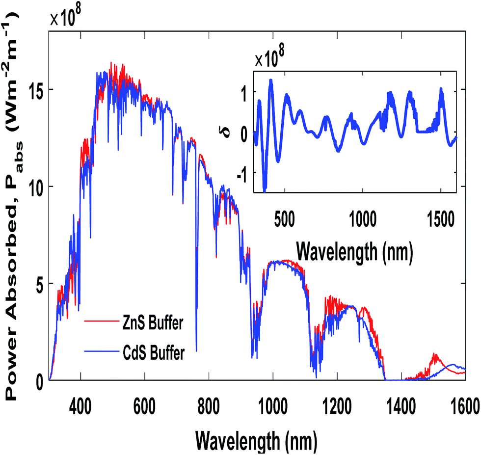
In closing, we studied the effect of buffer layer material on the performance of our proposed cell. As cadmium (Cd) is toxic and environment pollutant, from the industrial point of view, use of CdS should be as less as possible.63,64 ZnS, as an alternative buffer layer, could replace CdS because of its eco-friendly nature and cheap synthesis process.65 We investigated the performance of tandem cell with ZnS buffer layer instead of CdS at the optimized condition. Following the described optimization methodology, we matched the current densities of top and bottom cells by varying absorbers thickness (top cell's Jsc = 19.47 mA cm−2, bottom cell's Jsc = 19.89 mA cm−2). It was seen that the optimized thicknesses of CZTS and CZTSe with ZnS buffer layer had changed to 230 nm and 1200 nm, respectively. The same parameters listed in the Table 3 were used in the simulation. ZnS film has a band gap of ∼3.58 eV which is much higher than that of CdS (∼2.42 eV).55,57,58 Due to its higher band gap and lower extinction coefficient,66 most photons pass through the buffer layer without absorption, and able to reach to the main active layers. Thus, an increment in the thicknesses of main active layers was observed at the optimum condition compared to the previous case (CdS buffer). It is also found that the main absorbers utilize the solar spectrum slightly more efficiently at some wavelengths for ZnS buffer (Fig. 10). Moreover, the higher minority carrier mobility in ZnS (40 cm2 V−1 s−1) (CdS: 15 cm2 V−1 s−1) facilitates a higher collection efficiency of minority carriers. All these facts contribute to a higher Jsc when ZnS buffer layer is used. In addition, Voc also increases slightly due to higher optical absorption at the optimized condition. In total, 8% efficiency increment (relative) was observed when ZnS is used as buffer layer. Table 4 gives a comparison between the optimized performance of tandem cell with CdS and ZnS.
 |
| | Fig. 10 Comparison of absorbed power in the tandem cell with ZnS and CdS buffer layers. Inset shows the difference in absorbed power for the two cases [δ = Pabs(ZnS) − Pabs(CdS)]. | |
Table 4 Comparison between the optimized performance metrics of tandem cell with CdS and ZnS buffer layers
| Buffer layer |
Voc (V) |
Jsc (mA cm−2) |
FF |
Efficiency (%) |
| CdS |
1.431 |
19.17 |
0.726 |
19.86 |
| ZnS |
1.492 |
19.59 |
0.734 |
21.44 |
Conclusion
In summary, we analyzed the prospect of Cu2ZnSnS4/Cu2ZnSnSe4 tandem topology where both top and bottom cells have kesterite structures. CZTS and CZTSe absorbers were used to utilize the lower and higher wavelengths of solar spectrum, respectively. Thickness of the absorbers was also optimized for current matching condition of top and bottom cells and thereby best performance metrics were estimated. The maximum efficiency found from the calculation exceeds the previously proposed perovskite/kesterite tandem topology. In addition, the band gap analysis shows further enhancement in tandem efficiency when higher band gaps are used. Such enhancement is achievable due to the tunable property of kesterite. Finally, it was shown that replacing the CdS buffer layer with ZnS buffer layer leads to overall higher efficiency when the absorber layers are properly optimized. The proposed structure could make an eco-friendly, cheap all-kesterite solar cell with ηtandem ≥ 20%. The analysis presented in this regard would help in optimizing such tandem devices.
References
- M. Kumar, A. Dubey, N. Adhikari, S. Venkatesan and Q. Qiao, Energy & Environmental Science, 2015, 8, 3134–3159 CAS.
- S. López-Marino, Y. Sánchez, M. Espíndola-Rodríguez, X. Alcobé, H. Xie, M. Neuschitzer, I. Becerril, S. Giraldo, M. Dimitrievska and M. Placidi, J. Mater. Chem. A, 2016, 4, 1895–1907 Search PubMed.
- J. Oh, H.-C. Yuan and H. M. Branz, Nat. Nanotechnol., 2012, 7, 743–748 CrossRef CAS PubMed.
- S. C. Riha, B. A. Parkinson and A. L. Prieto, J. Am. Chem. Soc., 2011, 133, 15272–15275 CrossRef CAS PubMed.
- A. Shah, P. Torres, R. Tscharner, N. Wyrsch and H. Keppner, science, 1999, 285, 692–698 CrossRef CAS PubMed.
- M. A. Green, K. Emery, Y. Hishikawa, W. Warta and E. D. Dunlop, Prog. Photovoltaics, 2016, 24, 905–913 Search PubMed.
- A. Polizzotti, I. L. Repins, R. Noufi, S.-H. Wei and D. B. Mitzi, Energy & Environmental Science, 2013, 6, 3171–3182 CAS.
- J. J. Scragg, P. J. Dale, L. M. Peter, G. Zoppi and I. Forbes, Phys. Status Solidi B, 2008, 245, 1772–1778 CrossRef CAS.
- X. Liu, Y. Feng, H. Cui, F. Liu, X. Hao, G. Conibeer, D. B. Mitzi and M. Green, Progress in Photovoltaics: Research and Applications, 2016, 24, 879–898 CrossRef.
- S. Chen, X. Gong, A. Walsh and S.-H. Wei, Appl. Phys. Lett., 2010, 96, 021902 CrossRef.
- W. Wang, M. T. Winkler, O. Gunawan, T. Gokmen, T. K. Todorov, Y. Zhu and D. B. Mitzi, Adv. Energy Mater., 2014, 4, 1301465 CrossRef.
- L. Yin, G. Cheng, Y. Feng, Z. Li, C. Yang and X. Xiao, RSC Adv., 2015, 5, 40369–40374 RSC.
- D. B. Mitzi, O. Gunawan, T. K. Todorov, K. Wang and S. Guha, Sol. Energy Mater. Sol. Cells, 2011, 95, 1421–1436 CrossRef CAS.
- W. Wang, H. Shen, L. H. Wong, Z. Su, H. Yao and Y. Li, RSC Adv., 2016, 6, 54049–54053 RSC.
- K. Ito, Copper Zinc Tin Sulfide-Based Thin Film Solar Cells, John Wiley & Sons, Ltd, 2015 Search PubMed.
- T. P. Dhakal, C. Y. Peng, R. R. Tobias, R. Dasharathy and C. R. Westgate, Sol. Energy, 2014, 100, 23–30 CrossRef CAS.
- Y.-T. Hsieh, Q. Han, C. Jiang, T.-B. Song, H. Chen, L. Meng, H. Zhou and Y. Yang, Adv. Energy Mater., 2016, 6, 1502386 CrossRef.
- M. Neuschitzer, J. Marquez, S. Giraldo, M. Dimitrievska, M. Placidi, I. Forbes, V. Izquierdo-Roca, A. Pérez-Rodriguez and E. Saucedo, J. Phys. Chem. C, 2016, 120, 9661–9670 CAS.
- G. Y. Kim, D. H. Son, T. Thi Thu Nguyen, S. Yoon, M. Kwon, C. W. Jeon, D. H. Kim, J. K. Kang and W. Jo, Prog. Photovoltaics, 2016, 24, 292–306 CAS.
- B. Vermang, Y. Ren, O. Donzel-Gargand, C. Frisk, J. Joel, P. Salomé, J. Borme, S. Sadewasser, C. Platzer-Björkman and M. Edoff, IEEE J. Photovolt., 2016, 6, 332–336 CrossRef.
- F. Liu, C. Yan, J. Huang, K. Sun, F. Zhou, J. A. Stride, M. A. Green and X. Hao, Adv. Energy Mater., 2016, 6, 1600706 CrossRef.
- Y. Zhang, M. Ito, T. Tamura and A. Yamada, Appl. Phys. Express, 2011, 4, 052301 CrossRef.
- K. Sun, C. Yan, F. Liu, J. Huang, F. Zhou, J. A. Stride, M. Green and X. Hao, Adv. Energy Mater., 2016, 6, 1600046 CrossRef.
- C. Yan, F. Liu, K. Sun, N. Song, J. A. Stride, F. Zhou, X. Hao and M. Green, Sol. Energy Mater. Sol. Cells, 2016, 144, 700–706 CrossRef CAS.
- T. Todorov, T. Gershon, O. Gunawan, C. Sturdevant and S. Guha, Appl. Phys. Lett., 2014, 105, 173902 CrossRef.
- G. Niu, X. Guo and L. Wang, J. Mater. Chem. A, 2015, 3, 8970–8980 CAS.
- M. Batmunkh, C. J. Shearer, M. J. Biggs and J. G. Shapter, J. Mater. Chem. A, 2015, 3, 9020–9031 CAS.
- S. Ma, H. Zhang, N. Zhao, Y. Cheng, M. Wang, Y. Shen and G. Tu, J. Mater. Chem. A, 2015, 3, 12139–12144 CAS.
- A. Babayigit, D. D. Thanh, A. Ethirajan, J. Manca, M. Muller, H.-G. Boyen and B. Conings, Sci. Rep., 2016, 6, 18721 CrossRef CAS PubMed.
- F. Shao, L. Xu, Z. Tian, Y. Xie, Y. Wang, P. Sheng, D. Wang and F. Huang, RSC Adv., 2016, 6, 42377–42381 RSC.
- H. Azimi, Y. Hou and C. J. Brabec, Energy & Environmental Science, 2014, 7, 1829–1849 CAS.
- Z. Li, J. C. Ho, K. K. Lee, X. Zeng, T. Zhang, L. H. Wong and Y. M. Lam, RSC Adv., 2014, 4, 26888–26894 RSC.
- X. Lin, J. Kavalakkatt, M. C. Lux-Steiner and A. Ennaoui, Adv. Sci., 2015, 2, 1500028 CrossRef PubMed.
- J. Tao, K. Zhang, C. Zhang, L. Chen, H. Cao, J. Liu, J. Jiang, L. Sun, P. Yang and J. Chu, Chem. Commun., 2015, 51, 10337–10340 RSC.
- S.-Y. Kuo and M.-Y. Hsieh, Nanoscale, 2014, 6, 7553–7559 RSC.
- S. Bag, O. Gunawan, T. Gokmen, Y. Zhu, T. K. Todorov and D. B. Mitzi, Energy & Environmental Science, 2012, 5, 7060–7065 CAS.
- B. Shin, O. Gunawan, Y. Zhu, N. A. Bojarczuk, S. J. Chey and S. Guha, Prog. Photovoltaics, 2013, 21, 72–76 CAS.
- J. Ge, J. Chu, J. Jiang, Y. Yan and P. Yang, ACS Appl. Mater. Interfaces, 2014, 6, 21118–21130 CAS.
- C.-C. Liu, Y.-C. Liang, C.-C. Kuo, Y.-Y. Liou, J.-W. Chen and C.-C. Lin, Sol. Energy Mater. Sol. Cells, 2009, 93, 267–272 CrossRef CAS.
- H. Liu, Y. Tian, Y. Zhang, K. Gao, K. Lu, R. Wu, D. Qin, H. Wu, Z. Peng, L. Hou and W. Huang, J. Mater. Chem. C, 2015, 3, 4227–4234 RSC.
- H. Muguerra, G. Berthoux, W. Z. N. Yahya, Y. Kervella, V. Ivanova, J. Boucle and R. Demadrille, Phys. Chem. Chem. Phys., 2014, 16, 7472–7480 RSC.
- M. Bass, C. DeCusatis, J. Enoch, V. Lakshminarayanan, G. Li, C. Macdonald, V. Mahajan and E. Van Stryland, Handbook of optics, Volume II: Design, fabrication and testing, sources and detectors, radiometry and photometry, McGraw-Hill, Inc., 2009 Search PubMed.
- W. Bond, J. Appl. Phys., 1965, 36, 1674–1677 CrossRef CAS.
- M. Debenham, Appl. Opt., 1984, 23, 2238–2239 CrossRef CAS PubMed.
- M. Fang, A. Aristov, K. V. Rao, A. V. Kabashin and L. Belova, RSC Adv., 2013, 3, 19501–19507 RSC.
- C. A. Klein, Appl. Opt., 1986, 25, 1873–1875 CrossRef CAS PubMed.
- H. Li, J. Phys. Chem. Ref. Data, 1980, 9, 161–290 CrossRef CAS.
- E. D. Palik, Handbook of optical constants of solids, Academic press, 1998 Search PubMed.
- R. Treharne, A. Seymour-Pierce, K. Durose, K. Hutchings, S. Roncallo and D. Lane, 2011.
- J.-H. Lee, K.-H. Ko and B.-O. Park, J. Cryst. Growth, 2003, 247, 119–125 CrossRef CAS.
- S. Bag, O. Gunawan, T. Gokmen, Y. Zhu and D. B. Mitzi, Chem. Mater., 2012, 24, 4588–4593 CrossRef CAS.
- V. P. Devarajan, D. Nataraj, T. Pazhanivel, K. Senthil, M. Seol, K. Yong, J. Hermannsdorfer and R. Kempe, J. Mater. Chem., 2012, 22, 18454–18462 RSC.
- Z. Fan and J. G. Lu, J. Nanosci. Nanotechnol., 2005, 5, 1561–1573 CrossRef CAS PubMed.
- A. Janotti and C. G. Van de Walle, Rep. Prog. Phys., 2009, 72, 126501 CrossRef.
- A. Jha, S. K. Sarkar, D. Sen and K. Chattopadhyay, Nanoscale, 2015, 7, 2536–2544 RSC.
- S.-Y. Kuo and M.-Y. Hsieh, Nanoscale, 2014, 6, 7553–7559 RSC.
- J. Leitao, N. M. Santos, P. Fernandes, P. Salome, A. da Cunha, J. González, G. Ribeiro and F. Matinaga, Phys. Rev. B: Condens. Matter Mater. Phys., 2011, 84, 024120 CrossRef.
- O. Madelung, Semiconductors: data handbook, Springer Science & Business Media, 2012 Search PubMed.
- W. Martienssen and H. Warlimont, Springer handbook of condensed matter and materials data, Springer Science & Business Media, 2006 Search PubMed.
- D. P. Norton, Y. Heo, M. Ivill, K. Ip, S. Pearton, M. F. Chisholm and T. Steiner, Mater. Today, 2004, 7, 34–40 CrossRef CAS.
- G. Paul, S. Bandyopadhyay and S. Sen, Phys. Status Solidi A, 2002, 191, 509–518 CrossRef CAS.
- D. A. Neamen, Semiconductor Physics and Devices: Basic Principles, McGraw-Hill Education, 2012 Search PubMed.
- A. Bernard, Indian J. Med. Res., 2008, 128, 557 CAS.
- S. T. Hossain and S. K. Mukherjee, J. Hazard. Mater., 2013, 260, 1073–1082 CrossRef CAS PubMed.
- T.-H. Yeh, C.-H. Hsu, W.-H. Ho, S.-Y. Wei, C.-H. Cai and C.-H. Lai, Green Chem., 2016, 18, 5212–5218 RSC.
- A. Goudarzi, A. D. Namghi and C.-S. Ha, RSC Adv., 2014, 4, 59764–59771 RSC.
|
| This journal is © The Royal Society of Chemistry 2017 |
Click here to see how this site uses Cookies. View our privacy policy here. 
 Open Access Article
 This Open Access Article is licensed under a
  and
Md. Kawsar Alam
and
Md. Kawsar Alam
 distribution inside different layers. Each material was modeled by its respective refractive index (n) and extinction coefficient (κ) as a function of wavelength. Then, the absorbed power (Pabs) can be calculated from optical electric field distribution and imaginary part of complex dielectric constant as


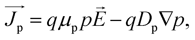
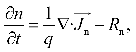
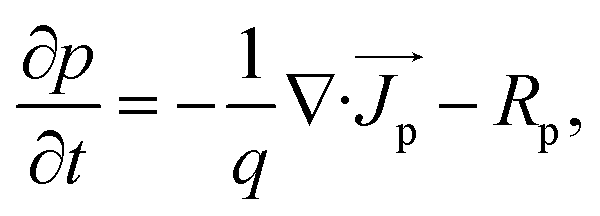
 is the electron (hole) current density, q is the positive electron charge, μn(p) is the mobility of electron (hole), Dn(p) is the diffusivity of electron (hole)
  , n and p are electron and hole densities, respectively, Rn(p) is the net recombination rate (the difference between the recombination rate and generation rate), kB is the Boltzmann constant and T is the temperature (the subscripts n and p indicate quantities that are specific to the carrier type). Generation rate calculated from the optical simulation was given as an input in the continuity equations and the equation set (eqn (4)–(8)) were solved self-consistently. In this way, we found the individual characteristics of top and bottom cells. We have used Lumerical FDTD and Device solvers for the optical and electrical simulations, respectively. The cells were modeled by the equivalent circuit shown in Fig. 2. In the circuit, Jph is the photon generated current density, Rs and Rsh represent series and shunt resistances, respectively. The current density through the diode, Jd can be calculated from: