
 Open Access Article
 This Open Access Article is licensed under a
 Creative Commons Attribution 3.0 Unported Licence
Formation of uniform PbS quantum dots by a spin-assisted successive precipitation and anion exchange reaction process using PbX2 (X = Br, I) and Na2S precursors†
Jin Hyuck Heo‡
ab,
Min Hyeok Jang‡a,
Min Ho Leea,
Myoung Sang Youa,
Sang-Wook Kimb,
Jae-Joon Leec and
Sang Hyuk Im *a
*a
aFunctional Crystallization Center (ERC), Department of Chemical Engineering, Kyung Hee University, Yongin-si, Gyeonggi-do, Republic of Korea. E-mail: imromy@khu.ac.kr
bDepartment of Molecular Science and Technology, Ajou University, Suwon 443-749, Republic of Korea
cDepartment of Energy & Materials Engineering, Dongguk University, Seoul, Republic of Korea
First published on 13th January 2017
Abstract
We devised a straightforward spin-assisted successive precipitation and anion exchange reaction (spin-SPAER) process in order to deposit relatively uniform PbS quantum dots (QDs) on mesoporous TiO2 (mp-TiO2). For the spin-SPAER process, we used PbX2 (X = I, Br, and Cl) precursors instead of a Pb(NO3)2 precursor and consequently deposited individual PbS QDs on mp-TiO2 due to the suppressed overgrowth of PbS QDs, whereas the conventional spin-assisted successive ionic layer adsorption and reaction (spin-SILAR) process formed aggregated PbS QDs on the mp-TiO2 surface due to continuous adsorption and reaction. In addition, the PbS QDs prepared by spin-SPAER showed better air stability than the PbS QDs prepared by spin-SILAR possibly due to the passivation by halogen elements such as I and Br. Accordingly, we could improve the overall power conversion efficiency of PbS QD-SSCs prepared by the spin-SPAER process using PbI2 and PbBr2 precursors to ∼26.7% and ∼44.2%, respectively, compared to the PbS QD-SSCs prepared by spin-SILAR using the Pb(NO3)2 precursor.
Metal chalcogenide, such as CdSe,1 CdTe,2 PbS,3 PbSe,4 Sb2S3,5 Sb2Se3,6 Sb2S3−xSex,7 HgTe,8 CISe2,9 and CITe2−xSex,10 semiconductor- or quantum dot (QD)-sensitizers have been considered as promising candidates replacing the conventional Ru/organic dye sensitizer because of their unique properties such as high absorptivity, convenient bandgap tailoring, easy charge separation by a large dipole moment, and solution processability.11
Among the metal chalcogenides, PbS QDs have been extensively studied because they are an ideal model light absorber due to their large Bohr radius, small bulk bandgap energy, strong absorptivity, wide absorption spectrum from visible to near infrared, and multiple exciton generation. PbS QD solar cells can be roughly classified as Schottky,12 depleted heterojunction,13 or sensitized type,14 with respect to the device architecture. Unlike Schottky and depleted heterojunction type devices, the sensitized solar cells have unique device architecture of electron conductor, sensitizer, and hole conductor, which can promptly transfer charge carriers into electron conductor and hole conductor. Occasionally the depleted heterojunction PbS QD solar cells exhibited higher device efficiency than the PbS QD-sensitized solar cells (QD-SSCs), the sensitized solar cells still have advantages to attain high efficiency with low cost in terms of device architecture and operating mechanism so that continuous studies are needed.
The PbS QD-SSCs are generally fabricated by depositing the PbS colloidal QDs (CQDs) on a mesoporous TiO2 (mp-TiO2) electron conductor or directly growing the PbS QDs on the mp-TiO2 via successive ionic layer adsorption and reaction (SILAR) method. The PbS CQDs have uniform size distribution so that they are good for injecting the electrons from PbS CQDs into mp-TiO2 because their conduction band edge can be uniformly positioned over the conduction band edge of mp-TiO2. However, their surfaces are passivated by insulating long alkyl chains in order to make uniform sized PbS CQDs via hot-injection method. Therefore, the insulating long alkyl ligands are replaced to short ligands such as 1,2-ethane dithiol (EDT), 3-mercaptopropionic acid (MPA), and halogens to improve the charge transport at mp-TiO2/PbS CQDs interface and PbS CQDs bulk. For instance, Im et al. reported 2.9% multiple-layered PbS QD-SSCs constructed by FTO/bl-TiO2 (blocking TiO2)/mp-TiO2/PbS CQDs/P3HT (poly-3-hexylthiophene)/PEDOT:PSS (poly(3,4-ethylenedioxythiophene) polystyrene sulfonate)/Au.15 Seo et al. reported 3.2% mesoporous PbS QD/CH3NH3PbI3 core/shell-SSCs.16 Kim et al. reported 3.9% PbS QD-SSCs with radial directional charge transport by using TiO2 nanorod electron conductor instead of mp-TiO2.17 Very recently, Park et al. reported 8.07% mesoporous PbS embedding CuS QD-SSCs.18
On the other hand, the PbS QDs prepared by SILAR method did not have any insulating passivation layer on their surface due to direct grown on the mp-TiO2. However, the SILAR method required tedious repeated process cycle: adsorption of cations (anions) → washing → drying → adsorption of anions (cations) → washing → drying. In addition, the size of PbS QDs deposited on mp-TiO2 surface is not uniform because some tiny PbS nanoparticles are nucleated and grown on the mp-TiO2 and at the same time the pre-deposited PbS nanoparticles are continuously overgrown by the repeated SILAR cycle, thereby deteriorating charge injection from PbS QDs into mp-TiO2. To reduce the tedious repeated process cycle, Joo et al. devised a spin-assisted SILAR (spin-SILAR) method for fabricating a liquid-junction CdS-sensitized ZnO nanorod photoelectrochemical cell.19 Im et al. reported the solid-state PbS-sensitized photovoltaic photodetectors and PbS–SSCs prepared by spin-SILAR.20 By using spin-coating process instead of dipping process, the washing and drying process could be eliminated because the excess chemicals are automatically spun out and the film is dried during spin-coating process. However, it is still difficult to control the size uniformity of PbS QDs deposited on mp-TiO2 via spin-SILAR. Therefore, here we tried to deposit more uniform PbS QDs on mp-TiO2 via spin-assisted successive precipitation and anion exchange reaction (spin-SPAER) because the over growth of the pre-deposited PbS QDs on mp-TiO2 can be reduced.
Fig. 1 is a schematic illustration of spin-SPARE process. For convention spin-SILAR, 5 mM Pb(NO3)2/H2O/methanol ionic solution was used so that the Pb2+ cations are adsorbed on mp-TiO2 surface and then Pb2+ cations are reacted with S2− anions to form PbS. During the repeated spin-SILAR process, the ions can be adsorbed on both mp-TiO2 and pre-deposited PbS QDs. Accordingly, the size of PbS nanoparticles formed on mp-TiO2 surface tends to be broadened as illustrated in upper right inset in Fig. 1 due to the formation of new PbS nuclei and the continuous overgrowth of pre-deposited PbS QDs. On the other hands, for spin-SPAER method 5 mM PbX2 (X = I, Br, and Cl)/DMF solution instead of 5 mM Pb(NO3)2/H2O/methanol ionic solution was spin-coated at 3000 rpm for 60 s. During the spin-coating process, the PbX2 nanoparticles are precipitated on the surface of mp-TiO2 (process I) as illustrated in Fig. 1. Then the PbX2 is transformed into PbS by anion exchange reaction with 5 mM Na2S/H2O/methanol solution during second stage spin-coating process (process II) at 3000 rpm for 60 s. To prevent the deposition/precipitation of PbX2 on pre-formed PbS on mp-TiO2, 1 wt% 1,2 ethanedithiol (EDT)/ethanol solution was spin-coated at 3000 rpm for 60 s. By the repetition of the spin-SAER process (process III), we expect that the individual PbS QDs will be formed on mp-TiO2 as illustrated in lower right inset in Fig. 1 because the PbX2 precipitates cannot adsorbed on the pre-formed PbS QDs unlike to Pb2+ cations.
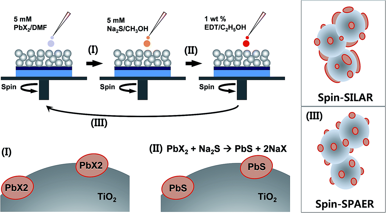 | ||
| Fig. 1 Schematic illustration of spin-assisted successive precipitation and anion exchange reaction (spin-SPARE) process. | ||
Fig. 2(a) is a photograph of 5 mM Pb(NO3)2/H2O/methanol ionic solution and PbX2 (X = I, Br, and Cl)/DMF solutions showing that Pb(NO3)2, PbI2, PbBr2 are well dissolved in H2O/methanol solution and DMF, respectively, whereas the 5 mM PbCl2 is precipitated in DMF due to poor solubility. The order of solubility of PbI2, PbBr2, and PbCl2 toward DMF solvent was PbI2 > PbBr2 > PbCl2. Therefore, we excluded the PbCl2/DMF solution for further model experiments. Fig. 2(b)–(d) are TEM (transmission electron microscopy) images of PbS nanoparticles deposited on mp-TiO2, which are fabricated by 15 times repeated cycles of spin-SPAER process with 5 mM of Pb(NO3)2/H2O/methanol ionic solution, PbI2/DMF, and PbBr2/DMF solution, respectively. The PbS nanoparticles deposited on mp-TiO2 from 5 mM of Pb(NO3)2/H2O/methanol ionic solution had polydispersed size (see Fig. 2(b)). Most PbS nanoparticles had below 5 nm but they are aggregated on mp-TiO2 and some PbS nanoparticles had over 5 nm in size. Accordingly the energetic electron injection from PbS nanoparticles into mp-TiO2 will be deteriorated by relatively large PbS nanoparticles because the conduction band edge of PbS nanoparticles with larger size become lower than the conduction band edge of mp-TiO2.21 On the other hands, the PbS QDs prepared from 5 mM PbI2/DMF and PbBr2/DMF solution showed smaller PbS nanoparticles with 3–5 nm in size (see Fig. 2(c and d)) and over grown PbS nanoparticles were not detected as shown in Fig. S1.† Apparently, the size PbS QDs deposited on mp-TiO2 from PbBr2/DMF solution seems to be slightly smaller than that from PbI2/DMF solution, which might be attributed to the quicker precipitation (nucleation) of PbBr2 than PbI2 during spin-coating process. It should be noted that the individual PbS QDs without over growth are formed on mp-TiO2 via spin-SPAER process as we proposed.
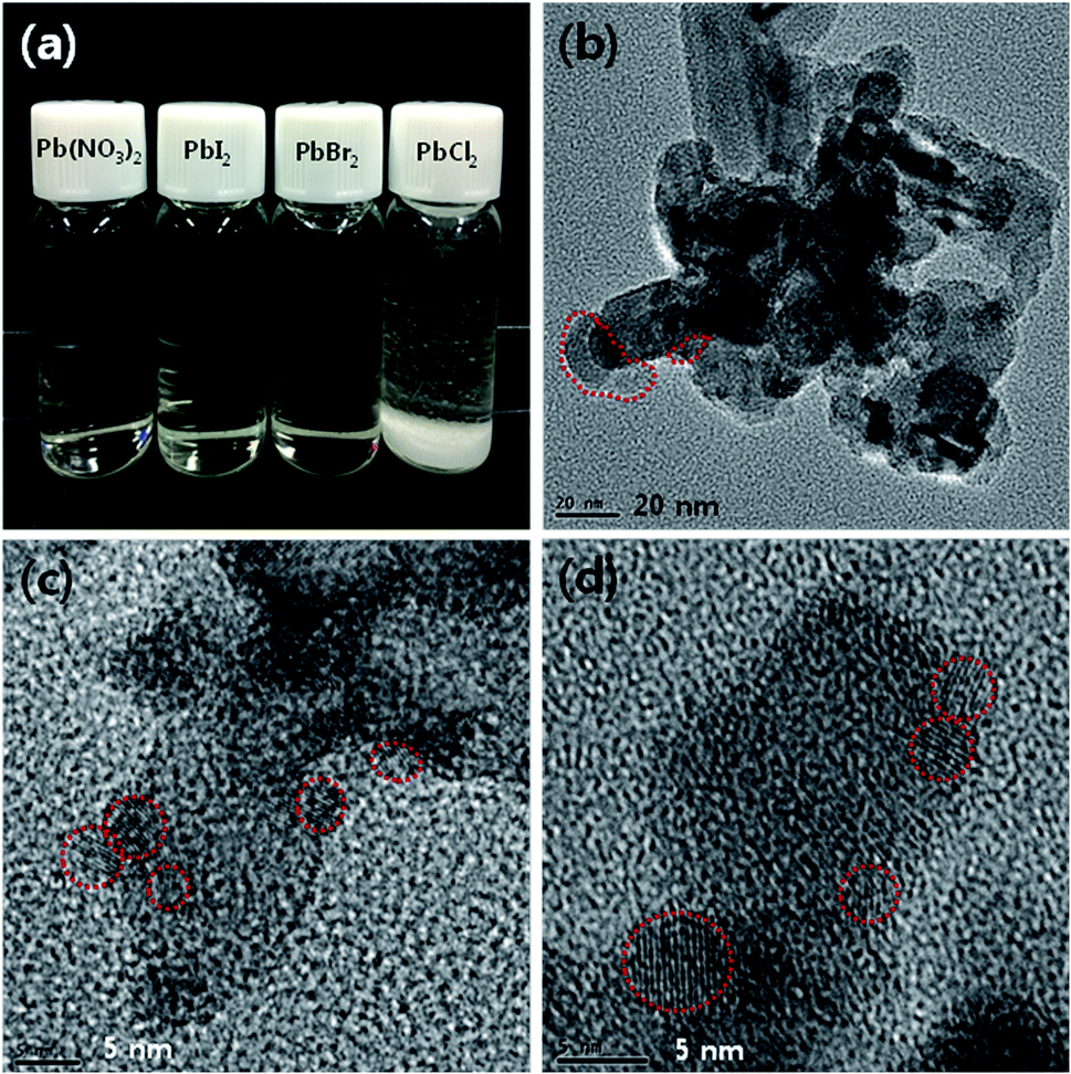 | ||
| Fig. 2 (a) A photograph of 5 mM Pb(NO3)2/H2O/methanol ionic solution and PbX2 (X = I, Br, and Cl)/DMF solutions and (b–d) TEM (transmission electron microscopy) images of PbS nanoparticles deposited on mp-TiO2, which are fabricated by 15 times repeated cycles of spin-SILAR process with 5 mM of Pb(NO3)2/H2O/methanol ionic solution (b) and spin-SPAER process with 5 mM of PbI2/DMF (c), and PbBr2/DMF solution (d), respectively. Red dotted region = PbS nanoparticles. | ||
Fig. 3(a) is a representative SEM (scanning electron microscopy) cross-sectional image of PbS QD-SSC of which the PbS QDs are prepared by 15 times repeated cycles of spin-SPAER process with 5 mM of PbBr2/DMF solution. The PbS QD-SSC was constructed by FTO/bl-TiO2 (∼50 nm in thickness)/mp-TiO2 (∼600 nm in thickness)/PbS QDs/P3HT (∼30 nm in thickness)/Au (∼60 nm in thickness). An energy band diagram of PbS QD-SSC was shown in Fig. 3(b). Upon illumination of light, the PbS QDs generate electron–hole pairs and the electrons (holes) are promptly transfer/transported into mp-TiO2 (P3HT), respectively. If the size of PbS QDs is fluctuated, the conduction band edge of PbS QDs is fluctuated so that the driving force of electron injection from PbS QDs into mp-TiO2 is dependent on the fluctuation. Fig. 3(c–e) compared the current density–voltage (J–V) curves of PbS QD-SSCs prepared by conventional spin-SILAR and newly proposed spin-SPAER process. Their photovoltaic properties were summarized in Table 1. To optimize efficiency of mode devices and check the tendency of the effect of spin-SPAER process, we fabricated PbS QD-SSCs with different repeated cycles for the formation of PbS QDs. For the model experiments, we controlled the repeated cycles of spin-SILAR and spin-SPAER to 10 (Fig. 3(c)), 15 (Fig. 3(d)), and 20 times (Fig. 3(e)), respectively. Irrespective to the repeated cycles for the formation of PbS QDs, the PbS QD-SSCs prepared by spin-SPAER process showed better device performance than that prepared by spin-SILAR process. The improved performance of PbS QD-SSCs prepared by spin-SPAER process is attributed to the formation of more uniform PbS-QDs on mp-TiO2. Eventually the PbS QD-SSCs prepared by 15 times repeated cycles of spin-SILAR and spin-SPAER process exhibited the best device performance. The Pb(NO3)2 sample prepared by spin-SILAR process showed 0.51 V open-circuit voltage (Voc), 12.5 mA cm−2 short-circuit current density (Jsc), 54% fill factor (FF), and 3.44% power conversion efficiency (η). The PbI2 and PbBr2 samples prepared by spin-SPAER process showed 0.59 V Voc, 13.2 mA cm−2 Jsc, 56% FF, and 4.36% η and 0.60 V Voc, 14.0 mA cm−2 Jsc, 59% FF, and 4.96% η at 1 Sun condition, respectively. Therefore, the best PbBr2 sample had improvement of 18% Voc, 12% Jsc, 9% FF, and 44% η compared to the Pb(NO3)2 device (see Table 1). The significant degradation of the performance in the PbS QD-SSCs with repeated coating cycles to 20 might be attributed to the formation of larger particles and the clogging of mesopores because the charge injection from large PbS sensitizer into mesoporous TiO2 will be significantly deteriorated by the mismatch of energy band and the hole extraction efficiency will be also greatly deteriorated by the ineffective infiltration of P3HT hole transporting material with the mesopores in mesoporous TiO2 film. Fig. 3(f) is EQE (external quantum efficiency) spectra of best devices (Fig. 3(d) samples). The calculated Jsc values from the integration of the EQE spectra of Pb(NO3)2, PbI2, and PbBr2 sample was 12.1, 13.0, and 13.7 mA cm−2, respectively so that these values were well matched to the measured Jsc values in J–V curves. The inset in Fig. 3(f) is the zoomed in EQE spectra around the band edge indicates that the onset wavelength of EQE spectrum is gradually blue-shifted in the order to Pb(NO3)2, PbI2, and PbBr2 sample. This implies that the average size of PbS QDs deposited on mp-TiO2 is gradually decreased in the order to Pb(NO3)2, PbI2, and PbBr2 sample. This result is consistent with the TEM analysis in Fig. 2(b–d). The electronic bandgap (Eg) of PbS QDs with a diameter (d) can be expressed by following equation.22
| Eg = 0.41 + 1/(0.025d2 + 0.283d) |
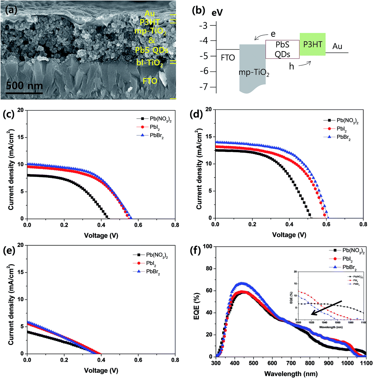 | ||
| Fig. 3 (a) SEM (scanning electron microscopy) cross-sectional image of representative PbS QD-SSC composed to FTO/bl-TiO2/mp-TiO2/PbS QDs/P3HT/Au:PbS QDs are formed by 15 times repeated spin-SPAER process with 5 mM PbBr2/DMF solution, (b) schematic energy band diagram, (c and d) current density–voltage (J–V) curves of PbS QD-SSCs with repeated coating cycles to (c) 10, (d) 15, and (e) 20 times of spin-SILAR (Pb(NO3)2) or spin-SPAER (PbI2, PbBr2) process, and (f) their corresponding EQE (external quantum efficiency) spectra: inset = zoom in at long wavelength region. | ||
| Repeated cycles | Device | Voc (V) | Jsc (mA cm−2) | FF (%) | η (%) |
|---|---|---|---|---|---|
| 10 | Pb(NO3)2 | 0.43 | 8.0 | 50 | 1.72 |
| PbI2 | 0.54 | 9.6 | 53 | 2.75 | |
| PbBr2 | 0.56 | 10.1 | 52 | 2.94 | |
| 15 | Pb(NO3)2 | 0.51 | 12.5 | 54 | 3.44 |
| PbI2 | 0.59 | 13.2 | 56 | 4.36 | |
| PbBr2 | 0.60 | 14.0 | 59 | 4.96 | |
| 20 | Pb(NO3)2 | 0.38 | 4.1 | 29 | 0.45 |
| PbI2 | 0.39 | 5.6 | 28 | 0.61 | |
| PbBr2 | 0.36 | 5.9 | 28 | 0.59 |
From above equation, the calculated average diameter of Pb(NO3)2, PbI2, and PbBr2 sample was over 3.7 nm, ∼3.6 nm, and ∼3.5 nm, respectively. The EQE is a product of light harvesting efficiency (ηlhe), charge separation efficiency (ηcs), and charge collection efficiency (ηcc). The absorption spectra of Pb(NO3)2, PbI2, and PbBr2 sample did not have significant difference (see Fig. S2†). Accordingly, the EQE improvement by newly designed spin-SPAER process was mainly ascribed to the improved charge separation efficiency (ηcs) and charge collection efficiency (ηcc).
In addition, the PbS QD-SSCs prepared by spin-SPAER process was much better air stability than the PbS QD-SSC prepared by spin-SILAR process. Therefore, we checked the XPS (X-ray photoelectron spectroscopy) spectra of PbS QDs prepared by 15 times repeated cycles of spin-SILAR (Pb(NO3)2 sample) and spin-SPAER process (PbI2 and PbBr2 sample) after 1 week storage in air in order to check the purity and stability of PbS QDs as shown in Fig. 4. The PbS QDs prepared by spin-SILAR process (Pb(NO3)2 sample) exhibited PbO peak from the analysis of Pb2p peak analysis, whereas the PbS QDs prepared by spin-SPAER process (PbI2 and PbBr2 sample) did not show oxide peaks. In contrast, the PbS QDs prepared by spin-SPAER process using PbI2 precursor exhibited PbI2 peaks, whereas the PbS QDs prepared by using PbBr2 precursor did not have PbBr2 peaks. To distinguish the PbO peaks and PbX2 (X = I, Br) peaks, we checked X3d peaks as shown in Fig. S3† because the binding energy of PbO and PbX2 in Pb2p peaks is very close. Fig. S3† clearly confirms that the small quantity of PbI2 was remained during spin-SPAER process, whereas the PbBr2 impurity peaks were not detectable due to fully conversion into PbS QDs. The S2p peaks in Fig. 4(d) confirm that the PbS QDs prepared by spin-SILAR process were oxidized to PbO and PbSO4, whereas the PbS QDs prepared by spin-SPAER were not oxidized. From these results, we can conclude that more efficient and stable PbS QD-SSCs could be fabricated by newly proposed spin-SPAER process.
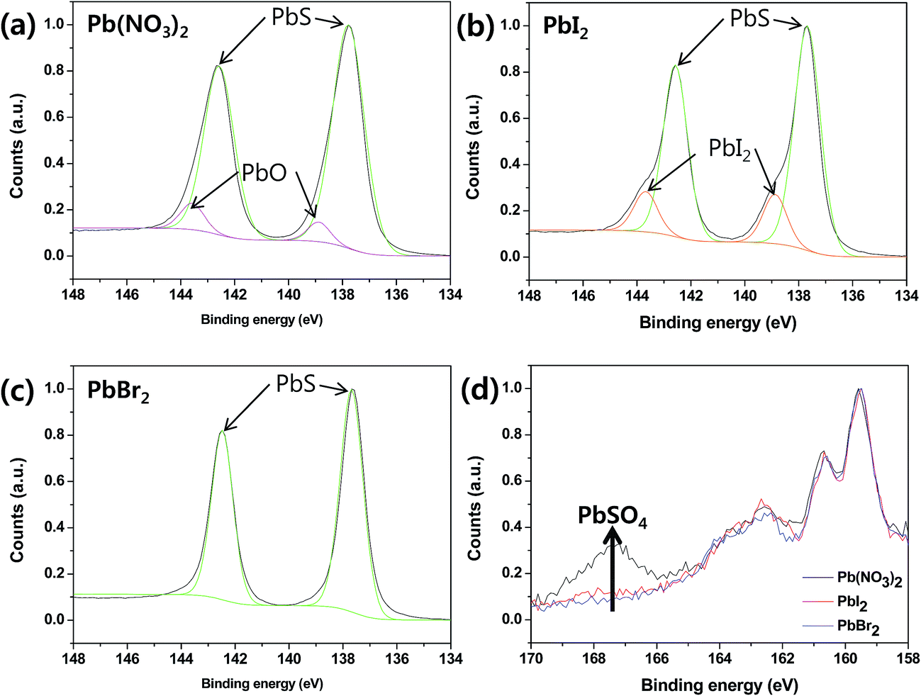 | ||
| Fig. 4 XPS (X-ray photoelectron spectroscopy) spectra Pb2p (a–c) and S2p (d) peaks of PbS prepared by (a) Pb(NO3)2, (b) PbI2, and (c) PbBr2. | ||
Conclusions
We could deposit relatively uniform PbS QDs via newly proposed spin-SPAER process whereas the conventional spin-SILAR process tends to form aggregated PbS QDs on mp-TiO2 surface. The formation of individual PbS QDs on mp-TiO2 by spin-SPAER might be attributed to the formation of nanoprecipitates of PbX2 (X = I, Br) so that the continuous over growth of PbS nanoparticles was suppressed. The solubility of PbI2 in DMF solvent was higher than the PbBr2 so that the size of nuclei of PbI2 formed during spin-coating process will be bigger than the that of PbBr2. Accordingly, the larger PbS QDs was formed by PbI2 precursor than the PbBr2. The EQE spectra of PbS QD-SSCs prepared by Pb(NO3)2, PbI2, and PbBr2 precursor indicated that the size of PbS QDs was gradually increased in the order to PbBr2 < PbI2 < Pb(NO3)2. Therefore, the overall power conversion efficiency of PbS QD-SSCs prepared by spin-SPAER process using PbI2 and PbBr2 precursor could be enhanced to ∼26.7% and ∼44.2%, respectively, compared to the PbS QD-SSCs prepared by spin-SILAR using Pb(NO3)2 precursor. From the XPS analysis, we could find that the PbS QD-SSCs prepared by spin-SPAER have better stability than the device prepared spin-SILAR because the surface of Pb or S in PbS QDs prepared by spin-SILAR is more easily oxidized into PbO or PbSO4 whereas the PbS QDs prepared by spin-SPAER are not easily oxidized possibly due to the passivation by I or Br element.Acknowledgements
This study was supported by Basic Science Research Program (No. 2014R1A5A1009799), the Priority Research Program (2009-0093826) through the National Research Foundation of Korea (NRF) funded by the Ministry of Science, ICT & Future Planning and the New & Renewable Energy Core Technology Program (No. 20133030000140) of the Korea Institute of Energy Technology Evaluation and Planning (KETEP) granted financial resource from the Ministry of Trade, Industry & Energy.Notes and references
- (a) H. J. Lee, M. K. Wang, P. Chen, D. R. Gamelin, S. M. Zakeeruddin, M. Grätzel and M. K. Nazeeruddin, Nano Lett., 2009, 9, 4221–4227 CrossRef CAS PubMed; (b) L. Qu and X. Peng, J. Am. Chem. Soc., 2002, 124, 2049–2055 CrossRef CAS PubMed; (c) I. Zarazúa, T. L. Luke, J. R. Gómez, A. T. Castro, J. Z. Zhang and E. D. l. Rosa, J. Electrochem. Soc., 2014, 161, H68–H74 CrossRef; (d) L. J. Diguna, Q. Shen, J. Kobayashi and T. Toyoda, Appl. Phys. Lett., 2007, 91, 23116 CrossRef; (e) C. B. Murray, D. J. Norris and M. G. Bawendi, J. Am. Chem. Soc., 1993, 115, 8706–8715 CrossRef CAS; (f) C. M. Donegá, S. G. Hickey, S. F. Wuister, D. Vanmaekelbergh and A. Meijerink, J. Phys. Chem. B, 2003, 107, 489–496 CrossRef.
- (a) G. Y. Lan, Z. Yang, Y. W. Lin, Z. H. Lin, H. Y. Liao and H. T. Chang, J. Mater. Chem., 2009, 19, 2349–2355 RSC; (b) C. S. Ferekides, D. Marinskiy, V. Viswanathan, B. Tetali, V. Palekis, P. Selvaraj and D. L. Morel, Thin Solid Films, 2000, 361, 520–526 CrossRef; (c) S. G. Kumar and K. S. R. K. Rao, Energy Environ. Sci., 2014, 7, 45–102 RSC; (d) J. Britt and C. Ferekides, Appl. Phys. Lett., 1993, 62, 2851–2852 CrossRef CAS; (e) A. M. Hermann, Sol. Energy Mater. Sol. Cells, 1998, 55, 75–81 CrossRef CAS.
- (a) R. J. Ellingson, M. C. Beard, J. C. Johnson, P. Yu, O. I. Micic, A. J. Nozik, A. Shabaev and A. L. Efros, Nano Lett., 2005, 5, 865–871 CrossRef CAS PubMed; (b) F. D. Monte, Y. Xu and J. D. Mackenzie, J. Sol-Gel Sci. Technol., 2000, 17, 37–45 CrossRef; (c) Y. Pan, Y. R. Li, Y. Zhao and D. L. Akins, J. Chem. Educ., 2015, 92, 1860–1865 CrossRef CAS; (d) H. Fu and S. W. Tsang, Nanoscale, 2012, 4, 2187–2201 RSC; (e) E. J. D. Klem, H. Shukla, S. Hinds, D. D. Macneil, L. Levina and E. H. Sargent, Appl. Phys. Lett., 2008, 92, 212105 CrossRef.
- (a) R. W. Crisp, D. M. Kroupa, A. R. Marshall, E. M. Miller, J. B. Zhang, M. C. Beard and J. M. Luther, Sci. Rep., 2015, 5, 9945 CrossRef CAS PubMed; (b) J. B. Zhang, J. B. Gao, C. P. Church, E. M. Miller, J. M. Luther, V. I. Klimov and M. C. Beard, Nano Lett., 2014, 14, 6010–6015 CrossRef CAS PubMed; (c) J. J. Choi, Y. F. Lim, M. B. S-Berrios, M. Oh, B. R. Hyun, L. F. Sun, A. C. Bartnik, A. Goedhart, G. G. Malliaras, H. D. Abruña, F. W. Wise and T. Hanrath, Nano Lett., 2009, 9, 3749–3755 CrossRef CAS PubMed; (d) X. Zhang, Y. Zhang, L. Yan, C. Y. Ji, H. Wu, Y. Wang, T. Q. Zhang, Y. D. Wang, T. Cui, J. Zhao and W. W. Yu, J. Mater. Chem. A, 2015, 3, 8501–8507 RSC; (e) M. Law, M. C. Beard, S. G. Choi, J. M. Luther, M. C. Hanna and A. J. Nozik, Nano Lett., 2008, 8, 3904–3910 CrossRef CAS PubMed.
- (a) D. H. Kim, S. J. Lee, M. S. Park, J. K. Kang, J. H. Heo, S. H. Im and S. J. Sung, Nanoscale, 2014, 6, 14549–14554 RSC; (b) Y. C. Choi, D. U. Lee, J. H. Noh, E. K. Kim and S. I. Seok, Adv. Mater., 2014, 24, 3587–3592 CAS; (c) Y. Itzhaik, O. Niitsoo, M. Page and G. Hodes, J. Phys. Chem. C, 2009, 113, 4254–4256 CrossRef CAS; (d) S. Ito, K. Tsujimoto, D. C. Nguyen, K. Manabe and H. Nichino, Int. J. Hydrogen Energy, 2013, 38, 16749–16754 CrossRef CAS; (e) N. Dematage, E. V. A. Premalal and A. Konno, Int. J. Electrochem. Sci., 2014, 9, 1729–1737 Search PubMed.
- (a) Y. Zhou, L. Wang, S. Chen, S. Qin, X. S. Liu, J. Chen, D. J. Xue, M. Luo, Y. Cao, Y. Cheng, E. H. Sargent and J. Tang, Nat. Photonics, 2015, 9, 409–415 CrossRef CAS; (b) L. Efthimiopoulos, J. Zhang, M. Kucway, C. Y. Park, R. C. Ewing and Y. Wang, Sci. Rep., 2013, 3, 2665 Search PubMed; (c) V. L. Deringer, R. P. Stoffel, M. Wuttig and R. Dronskowski, Chem. Sci., 2015, 6, 5255–5262 RSC; (d) F. A. E-Salam, M. Afifi and E. A. E-Wahabb, Vacuum, 1993, 44, 111–116 CrossRef; (e) X. Liu, J. Chen, M. Luo, M. Leng, Z. Xia, Y. Zhou, S. Qin, D. J. Xue, L. Lv, H. Huang, D. Niu and J. Tang, Appl. Mater. Interfaces, 2014, 6, 10687–10695 CrossRef CAS PubMed.
- (a) B. Yang, D. J. Xue, M. Leng, J. Zhong, L. Wang, H. Song, Y. Zhou and J. Tang, Sci. Rep., 2015, 5, 10978 CrossRef CAS PubMed; (b) Z. Xia, J. Zhong, M. Leng, L. Hu, D. J. Xue, B. Yang, Y. Zhou, X. Liu, S. Qin, Y. B. Cheng and J. Tang, Chem. Mater., 2015, 27, 8048–8057 CrossRef CAS.
- (a) M. Chen, L. Shao, S. V. Kershaw, H. Yu, J. Wang, A. L. Rogach and N. Zhao, ACS Nano, 2014, 8, 8208–8216 CrossRef CAS PubMed; (b) S. Keuleyan, E. Lhuillier and P. G. Sionnest, J. Am. Chem. Soc., 2011, 133, 16422–16424 CrossRef CAS PubMed; (c) S. Keuleyan, E. Lhuillier, V. Brajuskovic and P. G. Sionnest, Nat. Photonics, 2011, 5, 489–493 CrossRef CAS; (d) S. H. Im, H. J. Kin, S. W. Kim, S. W. Kim and S. I. Seok, Nanoscale, 2012, 4, 1581–1584 RSC; (e) M. Chen, H. Yu, S. V. Kershaw, H. Xu, S. Gupta, F. Hetsch, A. L. Rogach and N. Zhao, Adv. Mater., 2014, 24, 1032–1037 Search PubMed.
- (a) T. J. Gillespie, C. H. Marshall, M. Contreras and J. Keane, Sol. Energy Mater. Sol. Cells, 1999, 59, 27–34 CrossRef CAS; (b) J. W. Yang, J. Y. Kim, J. H. Yu, T. Y. Ahn, H. J. Lee, T. S. Choi, Y. W. Kim, J. Joo, M. J. Ko and T. G. Hyeon, Phys. Chem. Chem. Phys., 2013, 15, 20517–20525 RSC; (c) K. J. Kim, R. P. Oleksak, C. Pan, M. W. Knapp, P. B. Kreider, G. S. Herman and C. H. Chang, RSC Adv., 2014, 4, 16418–16424 RSC; (d) B. M. Basol, V. K. Kapur, A. Halani and C. Leidholm, Sol. Energy Mater. Sol. Cells, 1993, 29, 163–173 CrossRef CAS.
- S. W. Kim, M. J. Kang, S. J. Kim, J. H. Heo, J. H. Noh, S. H. Im, S. I. Seok and S. W. Kim, ACS Nano, 2013, 7, 4756–4763 CrossRef CAS PubMed.
- (a) A. J. Nozik, M. C. Beard, J. M. Luther, M. Law, R. J. Ellingson and J. C. Johnson, Chem. Rev., 2010, 110, 6873–6890 CrossRef CAS PubMed; (b) P. V. Kamat, J. Phys. Chem. C, 2008, 112, 18737–18753 CrossRef CAS; (c) B. Farrow and P. V. Kamat, J. Am. Chem. Soc., 2009, 131, 11124–11131 CrossRef CAS PubMed; (d) W. A. Tisdale, K. J. Williams, B. A. Timp, D. J. Norris, E. S. Andil and X. Y. Zhu, Science, 2010, 328, 1543–1547 CrossRef CAS PubMed; (e) R. D. Schaller and V. I. Klimov, Phys. Rev. Lett., 2004, 92, 186601 CrossRef CAS PubMed.
- (a) C. Piliego, L. Protesescu, S. Z. Bisri, M. V. Kovalenko and M. A. Loi, Energy Environ. Sci., 2013, 6, 3054–3059 RSC; (b) N. Zhao, T. P. Osedach, L. Y. Chang, S. M. Geyer, D. Wanger, M. T. Binda, A. C. Arango, M. G. Bawendi and V. Bulovic, ACS Nano, 2010, 4, 3743–3752 CrossRef CAS PubMed; (c) A. S. Obaid, A. A. Dihe, B. M. Salih, Z. Hassan, Y. Aldourin and M. Bououdina, Adv. Mater., 2014, 925, 605–609 Search PubMed.
- (a) A. G. P. Abraham, I. J. Kramer, A. R. Barkhouse, X. Wang, G. Konstantatos, R. Debnath, L. Levina, I. Raabe, M. K. Nazeeruddin, M. Grätzel and E. H. Sargent, ACS Nano, 2010, 4, 3374–3380 CrossRef PubMed; (b) M. Philip and N. Cowern, International Renewable and Sustainable Energy Conference, 2014, pp. 32–36 Search PubMed; (c) J. Shi, P. Zhao and X. Wang, Adv. Mater., 2013, 25, 916–921 CrossRef CAS PubMed; (d) M. M. Tavakoli, H. Aashuri, A. Simchi and Z. Fan, Phys. Chem. Chem. Phys., 2015, 17, 24412–24419 RSC; (e) B. A. Gonfa, H. Zhao, J. Li, J. Qiu, M. Saidani, S. Zhang, R. Izquierdo, N. Wu, M. A. E. Khakani and D. Ma, Sol. Energy Mater. Sol. Cells, 2014, 124, 67–74 CrossRef.
- (a) G. Niu, L. Wang, R. Gao, B. Ma, H. Dong and Y. Qiu, J. Mater. Chem., 2012, 22, 16914–16919 RSC; (b) S. D. Sung, L. S. Lim, P. Kang, C. M. Lee and W. I. Lee, Chem. Commun., 2013, 49, 6054–6056 RSC; (c) J. W. Lee, D. Y. Son, T. K. Ahn, H. W. Shin, I. Y. Kim, S. J. Hwang, M. J. Ko, S. H. Sul, H. S. Han and N. G. Park, Sci. Rep., 2013, 3, 1050 Search PubMed.
- S. H. Im, H. J. Kim, S. W. Kim, S. W. Kim and S. I. Seok, Energy Environ. Sci., 2011, 4, 4181–4186 CAS.
- G. S. Seo, J. W. Seo, S. C. Ryu, W. P. Yin, T. K. Ahn and S. I. Seok, J. Phys. Chem. Lett., 2014, 5, 2015–2020 CrossRef CAS PubMed.
- S. W. Kim, J. H. Heo, J. H. Noh, S. W. Kim, S. H. Im and S. I. Seok, ChemPhysChem, 2014, 15, 1024–1027 CrossRef CAS PubMed.
- J. P. Park, J. H. Heo, S. H. Im and S. W. Kim, J. Mater. Chem. A, 2015, 4, 785–790 Search PubMed.
- J. Joo, D. Kim, D. J. Yun, H. Jun, S. W. Rhee, J. S. Lee, K. Yong, S. Kim and S. Jeon, Nanotechnology, 2010, 21, 325604 CrossRef PubMed.
- S. H. Im, H. J. Kim, S. W. Kim, S. W. Kim and S. I. Seok, Org. Electron., 2012, 13, 2352–2357 CrossRef CAS.
- S. H. Im, H. J. Kim and S. I. Seok, Nanotechnology, 2011, 22, 395502 CrossRef PubMed.
- B. R. Hyun, Y. W. Zhong, A. C. Bartnik, L. Sun, H. D. AbruÇa, F. W. Wise, J. D. Goodreau, J. R. Matthews, T. M. Leslie and N. F. Borrelli, ACS Nano, 2008, 2, 2206–2212 CrossRef CAS PubMed.
Footnotes |
| † Electronic supplementary information (ESI) available. See DOI: 10.1039/c6ra25637f |
| ‡ These authors (J. H. Heo and M. H. Jang) have equally attributed to this work. |
| This journal is © The Royal Society of Chemistry 2017 |