
 Open Access Article
 This Open Access Article is licensed under a
 Creative Commons Attribution 3.0 Unported Licence
Biocompatible, optically transparent, patterned, and flexible electrodes and radio-frequency antennas prepared from silk protein and silver nanowire networks†
Kyungtaek Min‡
a,
Muhammad Umar‡a,
Haekyo Seob,
Jong Hyuk Yima,
Dong Gun Kamb,
Heonsu Jeonc,
Soonil Leead and
Sunghwan Kim*ad
aDepartment of Energy Systems Research, Ajou University, Suwon 16499, Republic of Korea. E-mail: sunghwankim@ajou.ac.kr
bDepartment of Electrical and Computer Engineering, Ajou University, Suwon 16499, Republic of Korea
cDepartment of Physics and Astronomy, Seoul National University, Seoul 08826, Republic of Korea
dDepartment of Physics, Ajou University, Suwon 16499, Republic of Korea
First published on 3rd January 2017
Abstract
Biological polymers offer new opportunities for flexible electronics, which are necessary for applications in soft and biological systems, because of their bio- and eco-friendly material traits. However, integrating an arbitrarily patterned electrode, the backbone of electronic devices, is still challenging when transparency of the electrode is required. Here, we report the fabrication of patterned silver nanowire (AgNW) networks buried at the surface of a silk fibroin film, which are suitable for bioelectronic applications that require biocompatibility, flexibility, high conductivity, and optical transparency. The AgNW-buried silk film exhibits excellent low sheet resistance of ∼15 Ω sq.−1 and high optical transparency of over 80%, along with smoothness of the surface. A light-emitting diode (LED) chip is successfully integrated on the patterned electrodes and can be stably turned on and off. Furthermore, we can produce a transparent resistor and a radio-frequency (RF) antenna on the silk film, and use them together as a food sensor that responds to the decreased conductivity caused by rancidity of spoiled food.
1. Introduction
Bioelectronics is defined as the study and application of electronics in biological systems. First discovered by Luigi Galvani in the 18th century, recent bioelectronic applications include electronic skins, biosensors for diabetics, and implantable pacemakers and defibrillators for damaged physiological functions.1–6 Since the most important function of bioelectronic devices is transducing signals across the biotic/abiotic interface,7,8 the field of bioelectronics has been limited by the availability and range of applicable materials at these interfaces in unconventional environments.9 Although complex and fast signal processing are available today owing to the revolution of silicon-based solid-state electronics, there is still a strong need to overcome the mismatch between rigid solid-state materials and soft biological surfaces. Hence, finding optimal materials remains one of the biggest challenges when designing bioelectronic devices with seamless biotic/abiotic interfaces.7Natural biomaterials are of particular interest to researchers because their material traits, such as flexibility, biocompatibility, biodegradability, and light weight, are favorable for bioelectronics.10,11 In particular, silk fibroin has been highly recognized for its strength in advanced fabrication and easy functionalization, as well as its bio-friendly material properties.12,13 Silk fibroin can be used for electronic passive components such as dissoluble substrates for conformal bioelectronics,14 resorbable substrates for biodegradable electronics,15,16 and precursors for energy storage.17 Taking the applications one step further, some groups have investigated using silk fibroin as active components in resistive-switching memory devices and organic field-effect transistors.18,19 In addition, optical transparency of the solidified silk films makes it possible for demonstrations of micro- and nanoscale optical components, as well as interesting approaches in opto-electronics.20–26
An important component of bioelectronic devices is a patterned conductor that is a backbone for the integration of electrical components and a functional component itself.27 With rapid advances in flexible and wearable electronic devices, extensive efforts have been made to develop new flexible and optically transparent conductors to replace conventional indium–tin oxide (ITO), a brittle and scarce material.28 A network of randomly connected silver nanowires (AgNWs) exhibits performance comparable to that of ITO and is regarded as the leading candidate to replace ITO among competitors that include conductive polymers, carbon nanotubes, graphene, and metal grids.28 Moreover, Ag is considered to be bio-friendly and suitable for bioelectronic devices not only in bulk form29 but also in the shape of nanowires.30 However, there are two critical issues for large-scale application of AgNW films: coarse surface and weak mechanical stability. These issues can be resolved by burying the network of AgNWs below the surface of an optically transparent polymer film.31 In this approach, silk fibroin is also used to yield an optically transparent conducting surface film and subsequently to integrate organic light-emitting diodes (OLEDs).32 The conducting silk surface films are useful for supporting conformal electronic and opto-electronic systems at the biological/electronic interface, when used in conjunction with the patterning scheme. Herein, we report the fabrication and characterization of optically transparent, flexible, patterned, and biocompatible electrodes by utilizing the AgNW networks buried at the surface of silk films; their application as a radio-frequency (RF) antenna is also presented. The AgNW-buried silk film exhibited low sheet resistance (Rs) of ∼15 Ω sq.−1 with an optical transmission (T) of 80% at 550 nm. Owing to the smoothness of a solidified silk surface and the strong adhesion between silk and Ag, we could obtain highly stable conductivity and even conductive surfaces that were suitable for integration and deposition of functional electrical and opto-electrical components. In addition, the good gas permeability of the silk matrix made it possible to affect the conductivity of the AgNW network with reactable gases, and this scheme was applied in food sensor technology by monitoring the conductivity of a line electrode and the resonant response of a radio-frequency (RF) antenna.
2. Experimental
2.1. Preparation of silk aqueous solution
Bombyx mori cocoons were boiled in a solution of 0.02 M Na2CO3 for 45 min to remove the sericin protein. The remaining fibroin fibers were rinsed with distilled water and then dried in air for 24 h. The dried fibroin fibers were dissolved in a 9.3 M LiBr solution at 60 °C for 4 h to obtain an aqueous solution with fibroin concentration of 20 wt%. For 2 days, the silk–LiBr solution was dialyzed against distilled water using a dialysis cassette (molecular weight cut off, MWCO: 3.5 K; Slide-a-Lyzer, Thermo Scientific) at room temperature. The final concentration of silk fibroin was 6 wt%. Before use, the obtained solution was purified using a centrifuge and a syringe filter with a pore size of 0.45 μm to remove impurities.2.2. Fabrication process
To yield AgNW layers, the AgNW aqueous solution (0.3 wt%, DK5IP-2, Nanopyxis Co., Ltd.) was spin-coated on bare and resist-patterned silicon substrates. The density of AgNWs was controlled by the spinning speed, which was set to 500, 1000, 1500, and 2000 rpm to produce a AgNW density of 73.5, 33.8, 21.3, and 19.3 mg m−2, respectively. For better adhesion between the AgNWs and silicon, the AgNW-coated silicon substrate was baked at 100 °C for 5 min. In order to transfer the AgNW sheet to a silk film, the aqueous silk solution was poured on the AgNW-coated silicon substrate and the substrate was left to dry for 24 h. After casting, the silk film was detached in isopropanol. To create a patterned AgNW network, we first prepared a photoresist (DNR L300-30, Dongjin Semichem) pattern on the silicon substrate. The AgNW aqueous solution was spin-coated on the photoresist pattern and then the patterned photoresist layer was removed using acetone to yield the patterned AgNW network. Finally, we transferred the patterned AgNW network to the silk film by casting.2.3. Characterization of the AgNW-buried silk films
The transmission of light in the AgNW-buried silk films was measured by an optical set-up utilizing a broadband white light source and a photospectrometer (V-670, JASCO). We used four-point probe resistance measurements (Model 280, Four Dimensions Inc.) to investigate the sheet resistance of the AgNW layers. Using a network analyzer (37247D, Anritsu), the electromagnetic reflection of the AgNW–silk RF antenna was analyzed through the impedance matching phenomenon. Prior to the measurements, the analyzer was calibrated to reduce errors in the reflection measurements, such as directivity, source match, and frequency tracking, and ensure better frequency response of the AgNW RF antenna. The resistance of the patterned AgNW layer was measured with a digital multimeter (DM-334).3. Results and discussion
A schematic representation of our approach is shown in Fig. 1. Silk fibroin, a natural protein extracted from Bombyx mori cocoons, was used to yield a free-standing film with favorable traits such as biocompatibility, environment friendliness, optical transparency, mechanical stability, and flexibility.12 The insulating surface of the silk film could be modified to possess electrical conductivity by burying the AgNW network just beneath the surface. In addition, the AgNW network could be arbitrarily patterned, thereby acting as an electrode and an RF antenna. The AgNWs used had an average diameter of 40 nm and an average length of about 20 μm. The fabrication of the AgNW-buried silk surface conductor is described in Experimental section and Fig. S1.† In brief, an aqueous AgNW solution was spin-coated on the patterned photoresist and the exposed photoresist was removed in acetone. We then cast the aqueous silk solution over the patterned AgNW network. During the process, silk proteins infiltrated the openings of the network and reached the silicon surface to produce a smooth silk/silicon interface. After drying in air, the solidified silk film was peeled off the silicon surface with the patterned AgNW network. As revealed in Fig. 1, by patterning a loop, we could obtain an optically transparent and free-standing RF antenna with all the favorable material traits of silk fibroin and AgNWs.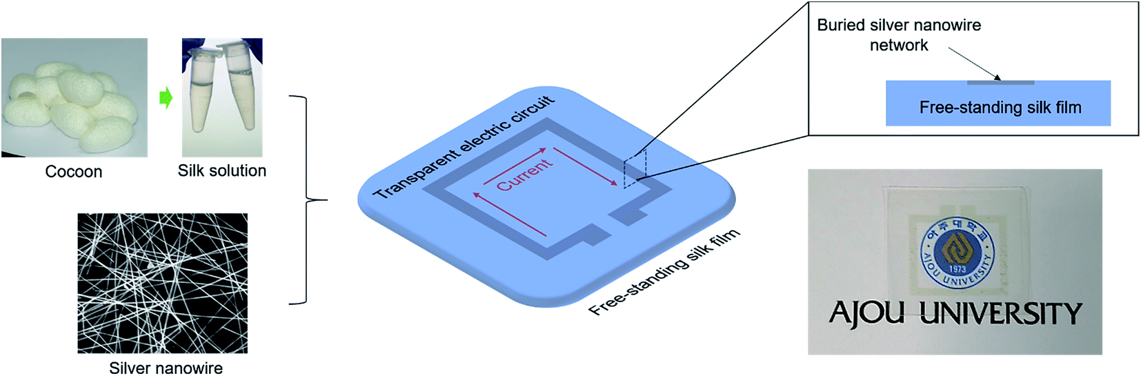 | ||
| Fig. 1 Schematic diagram showing a patterned, optically transparent, flexible, and biocompatible surface conductor prepared from silk fibroin and silver nanowires (AgNWs). The patterned AgNW network was buried at the surface of the free-standing silk film and exhibits optical transparency and good electrical conductivity. The electric current could flow through the buried AgNW surface conductor, and this setup can be used as an electrode and a radio-frequency (RF) antenna. | ||
Fig. 2a–d show images obtained with a scanning electron microscope (SEM) and an atomic force microscope (AFM) for investigating the morphology of the AgNW-buried silk surface. The spin-coated AgNWs formed well-distributed and intercrossed AgNW networks on the silicon substrate (Fig. 2a) and at the surface of the silk film (Fig. 2b). However, since the SEM method produces images of a sample using scattered electrons that interact with atoms in the sample, the conductivity of each material affects the contrast of the images. This means that it is difficult to estimate the three-dimensional morphology of a material from two-dimensional SEM images. Therefore, we took advantage of the AFM method to determine the surface morphology. As shown in Fig. 2c and d, the surface roughness (root-mean-square value) was significantly reduced from 12.67 nm (AgNWs on silicon) to 2.35 nm (AgNWs buried in silk), which is comparable to the value of commercial ITO/polyethylene-naphthalate (PEN) substrates (∼3.4 nm) and other AgNW-buried polymer surfaces.33 Unlike the coarse and sparse AgNW layer on silicon, a smooth and solid conductive surface could be obtained for the buried AgNWs at the surface of the silk film.
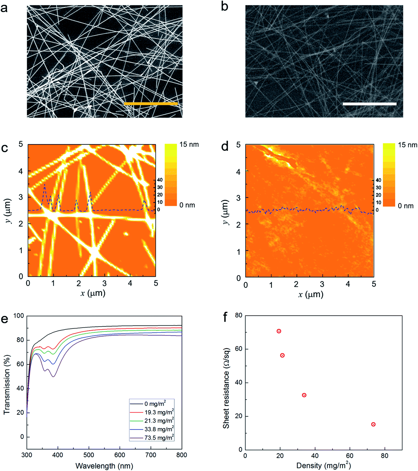 | ||
| Fig. 2 Scanning electron microscope (SEM) images showing the morphology of (a) AgNWs on bare silicon and (b) AgNWs buried at a density of 21.3 mg m−2 at the surface of a silk film. Surface morphology images and section curves (blue dashed) obtained using an atomic force microscope (AFM): (c) surface shown in (a); (d) surface shown in (b). (e) Ultraviolet-visible-near-infrared (UV-vis-NIR) transmission spectra and (f) sheet resistance of the AgNW–silk films at different AgNW densities. The scale bars in (a) and (b) correspond to a length of 5 μm. | ||
High T and low Rs, which were simultaneously obtained, are important advantages of the AgNW-buried silk surface conductor. As shown in Fig. 2e, high optical transparency (T > 80%) was obtained over a broad spectral range of 450–850 nm. Although the plasmonic absorption of AgNWs in the UV region occurred, the AgNW electrodes satisfy the requirement of the spectral window of transparency, which can be defined by the eye luminosity curve (for light-emitting devices) or the spectral irradiance from the sun (for solar cell applications).28 As expected, the increased density of AgNWs reduced the T and Rs values (Fig. 2e and f). The value of T at 550 nm was 89.1%, with Rs of 70.7 Ω sq.−1 and a density of 19.3 mg m−2, whereas a transparent film with T of 83.6% had Rs of 15.2 Ω sq.−1 at a density of 73.5 mg m−2. These values are comparable to those of commercially available ITO electrodes on plastic substrates and those of AgNW electrodes buried in polymers.33 In addition, we investigated T versus Rs trade-off characteristics, qualified in terms of the ratio σdc/σop in the Tinkham formula:34
To demonstrate the usefulness of patterned AgNW networks in electronic devices, we designed and fabricated a simple LED circuit and a loop RF antenna; its operation is shown in Fig. 3. After preparation of two AgNW line electrodes, a commercial LED chip was mounted on the electrodes using solder, and it could be turned on through the transparent electrodes (Fig. 3a). Fig. 3b shows the current–voltage (I–V) curves of the LED circuits operating on the AgNW line electrodes with different densities and lengths. The as-fabricated LEDs on the AgNW electrodes exhibited ideal operation with a turn-on voltage of 2.4 V, exactly the same as specified for the commercial chip. The slopes of the I–V curves, reflecting the overall resistance of the circuit system, were identical for the circuits with the same AgNW density despite their differing line-lengths. When the density of the AgNWs was decreased, the LED circuit exhibited slightly reduced luminance, which can be attributed to the increased resistivity of the AgNW electrodes. Additionally, no degradation during continued operation or degradation as a result of multiple on/off cycles was observed.
 | ||
| Fig. 3 (a) Operation of an LED chip on AgNW line electrodes. The dashed rectangular boxes indicate the patterned AgNW electrodes. (b) Current–voltage characteristics of the LED circuits with different densities of AgNWs and lengths of line electrodes. All circuits turned on the LEDs at 2.4 V, the same as shown in the specification. (c) Photograph of a loop RF antenna on a curved surface. (d) Return loss (S11) of the antenna before (blue line) and after (red line) bending. After bending, the RF antenna exhibited higher resonant frequency. | ||
We designed and fabricated a loop RF antenna based on silk fibroin and the AgNW network layer (Fig. S5a†). A rectangular loop antenna was designed to resonate at 10 GHz, as shown in Fig. 1. The antenna structure was simulated with HFSS using lumped-port excitation at the feeding point. The reflected electromagnetic (EM) power of the antenna was characterized with a vector network analyzer and compared with the simulated spectrum (Fig. S5b†). The measured resonant frequencies were located at 5.5 GHz (corresponding to the half-wavelength) and 10.5 GHz (the quarter-wavelength), which were slightly higher than the simulated values. The return losses, also known as S11, were −15.5 and −19.5 dB, which are much lower than those of the simulated values, along with the higher Q factors (the narrower bandwidths). These results indicate that more than 97.2% power was transmitted at the resonant frequencies. It should be noted that the differences between the simulation and the experiments results originated from the fabrication tolerances, scarce information for the dielectric constant of silk fibroin, and poor conductivity value used in the simulation. To apply the proposed RF antennas in bio- or wearable electronics, investigations on the effect of flexibility of the fabricated RF antennas are necessary. Fig. 3c shows a photograph of the bended RF antenna on a curved surface with a radius of curvature of 30 mm. Since bending a flat RF antenna reduces the effective length of the antenna, the resonant frequency increased as expected (corresponding to the blue-shifted wavelength) (Fig. 3d). To confirm the increased frequency resulting from bending, a simulation considering a curved RF antenna was performed, and the results showed increased frequencies for both resonances (Fig. S6b†). These increase margins in the reflection spectrum could be influenced by the curvature of the curved RF antenna because the larger curvature induced a larger decrease in the effective antenna size. Fig. S7† exhibits a plot of S11 for a radius of curvature of 90 mm, which is larger than that shown in Fig. 3d. Although the resonant frequency was increased by bending, we confirmed that the increase margin for the 90 mm curvature was smaller than that for the 30 mm curvature, indicating the larger effective antenna size. Furthermore, the mechanical stability of the RF antenna represents an advantage of our approach. As revealed in Fig. S6a,† the resonant frequency and the reflectance were consistently preserved during the repeated bending and unbending.
Evaluation of food quality is an important issue all over the world, as it is directly related to public health and the food industry. Along with its use as an antimicrobial agent in food and beverages, Ag also has a long history as a poison indicator in foods, which originates from the tarnishing of a Ag surface due to its reaction to sulfur. Odor from spoiled food also contains hydrogen sulfide (H2S),39 which can induce corrosion of a Ag surface40 and decrease its electrical conductivity through the formation of Ag2S.41 To confirm that the electrical conductivity of AgNWs was deteriorated by the odor from spoiled food, a piece of glass coated with a layer of AgNWs was exposed to odor from a slice of spoiled chicken in an enclosed box. After the exposure, the sheet resistance of the AgNW-coated glass increased from 60 to 95 Ω sq.−1, and a corrugated surface was observed, as shown in Fig. S8.† To explore potential applications of AgNWs, the patterned AgNW electrode and RF antenna in the silk film were used as a single-use food sensor (Fig. 4a), which can be applied to a vinyl or plastic food package. As shown in Fig. 4b, the electrical resistance of a line electrode increased with increasing exposure to the odor of the spoiled chicken, while the electrical resistance of a line electrode exposed to fresh chicken was well-preserved. After the line electrode was exposed to the spoiled chicken for 1 h, the resistance almost tripled. An increase in resistance has an effect on the resonance quality of an RF antenna. We used the patterned AgNW RF antenna with S11 of −18.45 dB at a resonant frequency of 10.85 GHz for the food sensing. The increased resistance of the AgNW network after 30 min of odor-exposure induced a 2.45 dB reduction in transmittance, which corresponds to a 1.1% reduction in the transmitted power (Fig. 4c). In both cases, the proof-of-concept experiments exhibited reliable sensitivities to spoiled food. As an added advantage, the surface chemistry of Ag to provide selectivity for analytes and integration of another functional optical or electrical device would expand the range of applications in biological and environmental sciences.
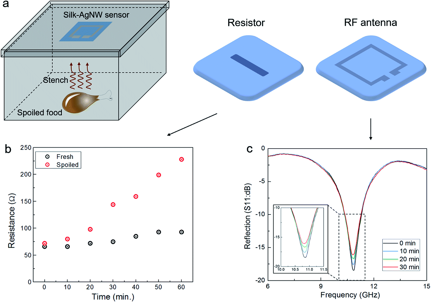 | ||
| Fig. 4 (a) Schematic image showing an application of a silk–AgNW line resistor and RF antenna as a food sensor. Spoiled chicken was used to emit the foul odor. (b) Experimentally measured time-dependent resistance of a line electrode and (c) reflections of an RF antenna applied to a slice of rancid chicken. | ||
4. Conclusions
We demonstrated the fabrication of patterned, optically transparent, flexible, and biocompatible surface conductors by embedding AgNWs just below the surface of the silk fibroin film. The conducting silk surface films exhibited high optical transparency (∼80%) and low sheet resistance (∼15 Ω sq.−1) simultaneously, along with superior mechanical robustness and an ultra-smooth surface. The use of conventional photolithography for the fabrication means that it has a low cost of operation and could be extended to support large-scale production. We could apply this approach to a patterned circuit board to integrate a commercial LED chip and a RF antenna for wireless communications. The line electrodes and RF antennas were applied as single-use food sensors to detect odor from spoiled food, which induced the diminished conductivities of the AgNW networks. Furthermore, bio-friendly traits of silk fibroin, such as biocompatibility, biodegradability, and ease of biofunctionalization, can lead to new applications at the interface between a biological surface and a bioelectronic or optoelectronic device.Acknowledgements
K. M. and M. U. contributed equally to this work. This work was supported by the National Research Foundation (NRF) of Korea grants funded by the Korean government (grant no. 2014R1A1A1008080, 2016R1D1A1B03933510, 2014R1A2A1A11051576).References
- S. Bauer, Nat. Mater., 2013, 12, 871 CrossRef CAS PubMed.
- J. J. Boland, Nat. Mater., 2010, 9, 790 CrossRef CAS PubMed.
- C. Wang, D. Hwang, Z. Yu, K. Takei, J. Park, T. Chen, B. Ma and A. Javey, Nat. Mater., 2013, 12, 899 CrossRef CAS PubMed.
- M. L. Hammock, A. Chortos, B. C.-K. Tee, J. B.-H. Tok and Z. Bao, Adv. Mater., 2013, 25, 5997 CrossRef CAS PubMed.
- K. MacVittie, J. Halamek, L. Halamkova, M. Southcott, W. D. Jemison, R. Lobeld and E. Katz, Energy Environ. Sci., 2013, 6, 81 CAS.
- S. Carrara, S. Ghoreishizadeh, J. Olivo, I. Taurino, C. Baj-Rossi, A. Cavallini, M. Op de Beeck, C. Dehollain, W. Burleson, F. G. Moussy, A. Guiseppi-Elie and G. De Micheli, Sensors, 2012, 12, 11013 CrossRef CAS PubMed.
- J. Rivnay, R. M. Owens and G. G. Malliaras, Chem. Mater., 2014, 26, 679 CrossRef CAS.
- J. Du, C. Catania and G. C. Bazan, Chem. Mater., 2014, 26, 686 CrossRef CAS.
- M. Muskovich and C. J. Bettinger, Adv. Healthcare Mater., 2012, 1, 248 CrossRef CAS PubMed.
- M. Irimia-Vladu, Chem. Soc. Rev., 2014, 43, 588 RSC.
- A. Lendlein and R. Langer, Science, 2002, 296, 1673 CrossRef PubMed.
- H. Tao, D. L. Kaplan and F. G. Omenetto, Adv. Mater., 2012, 24, 2824 CrossRef CAS PubMed.
- B. Zhu, H. Wang, W. R. Leow, Y. Cai, X. J. Loh, M.-Y. Han and X. Chen, Adv. Mater., 2015, 28, 4250 CrossRef PubMed.
- D.-H. Kim, J. Viventi, J. J. Amsden, J. Xiao, L. Vigeland, Y.-S. Kim, J. A. Blanco, B. Panilaitis, E. S. Frechette, D. Contreras, D. L. Kaplan, F. G. Omenetto, Y. Huang, K.-C. Hwang, M. R. Zakin, B. Litt and J. A. Rogers, Nat. Mater., 2010, 9, 511 CrossRef CAS PubMed.
- S.-W. Hwang, H. Tao, D.-H. Kim, H. Cheng, J.-K. Song, E. Rill, M. A. Brenckle, B. Panilaitis, S. M. Won, Y.-S. Kim, Y. M. Song, K. J. Yu, A. Ameen, R. Li, Y. Su, M. Yang, D. L. Kaplan, M. R. Zakin, M. J. Slepian, Y. Huang, F. G. Omenetto and J. A. Rogers, Science, 2012, 28, 1640 CrossRef PubMed.
- H. Tao, S.-W. Hwang, B. Marelli, B. An, J. E. Moreau, M. Yang, M. A. Brenckle, S. Kim, D. L. Kaplan, J. A. Rogers and F. G. Omenetto, Proc. Natl. Acad. Sci. U. S. A., 2014, 111, 17385 CrossRef CAS PubMed.
- Y. S. Yun, S. Y. Cho, J. Shim, B. H. Kim, S.-J. Chang, S. J. Baek, Y. S. Huh, Y. Tak, Y. W. Park, S. Park and H.-J. Jin, Adv. Mater., 2013, 25, 1993 CrossRef CAS PubMed.
- H. Wang, F. Meng, B. Zhu, W. R. Leow, Y. Liu and X. Chen, Adv. Mater., 2015, 27, 7670 CrossRef CAS PubMed.
- C.-H. Wang, C.-Y. Hsieh and J.-C. Hwang, Adv. Mater., 2011, 23, 1630 CrossRef CAS PubMed.
- H. Kwon and S. Kim, ACS Photonics, 2015, 2, 1675 CrossRef CAS.
- M. Lee, H. Jeon and S. Kim, Nano Lett., 2015, 15, 3358 CrossRef CAS PubMed.
- S. Kim, A. N. Mitropoulos, J. D. Spitzberg, H. Tao, D. L. Kaplan and F. G. Omenetto, Nat. Photonics, 2012, 6, 818 CrossRef CAS.
- B. Lee, H. Kwon, S. Kim and F. Rotermund, Opt. Mater. Express, 2016, 6, 993 CrossRef.
- Y. Y. Diao, X. Y. Liu, G. W. Toh, L. Shi and J. Zi, Adv. Funct. Mater., 2013, 23, 5373–5380 CrossRef CAS.
- S. T. Parker, P. Domachuk, J. Amsden, J. Bressner, J. A. Lewis, D. L. Kaplan and F. G. Omenetto, Adv. Mater., 2009, 21, 1 Search PubMed.
- M. B. Applegate, B. P. Partlow, J. Coburn, B. Marelli, C. Pirie, R. Pineda, D. L. Kaplan and F. G. Omenetto, Adv. Mater., 2016, 28, 2417 CrossRef CAS PubMed.
- S. H. Park, Y. J. Kang and S. Majd, Adv. Mater., 2015, 27, 7583 CrossRef CAS PubMed.
- K. Ellmer, Nat. Photonics, 2012, 6, 808 CrossRef.
- J. R. Morones-Ramirez, J. A. Winkler, C. S. Spina and J. J. Collins, Sci. Transl. Med., 2013, 5, 190ra81 Search PubMed.
- N. K. Verma, J. Conroy, P. E. Lyons, J. Coleman, M. P. O'Sullivan, H. Kornfeld, D. Kelleher and Y. Volkov, Toxicol. Appl. Pharmacol., 2012, 264, 451–461 CrossRef CAS PubMed.
- X.-Y. Zeng, Q.-K. Zhang, R.-M. Yu and C.-Z. Lu, Adv. Mater., 2010, 22, 4484 CrossRef CAS PubMed.
- Y. Liu, Y. Xie, Y. Liu, T. Song, K.-Q. Zhang, L. Liao and B. Sun, Semicond. Sci. Technol., 2015, 30, 104004 CrossRef.
- K.-H. Ok, J. Kim, S.-R. Park, Y. Kim, C.-J. Lee, S.-J. Hong, M.-G. Kwak, N. Kim, C. J. Han and J.-W. Kim, Sci. Rep., 2015, 5, 9464 CrossRef CAS PubMed.
- D. S. Hecht, L. Hu and G. Irvin, Adv. Mater., 2011, 23, 1482 CrossRef CAS PubMed.
- D. Alemu, H.-Y. Wei, K.-C. Ho and C.-W. Chu, Energy Environ. Sci., 2012, 5, 9662 CAS.
- J. H. Yim, S.-Y. Joe, C. Pang, K. M. Lee, H. Jeong, J.-Y. Park, Y. H. Ahn, J. C. de Mello and S. Lee, ACS Nano, 2014, 8, 2857 CrossRef CAS PubMed.
- S. Ye, A. R. Rathmell, Z. Chen, I. E. Stewart and B. J. Wiley, Adv. Mater., 2014, 26, 6670–6687 CrossRef CAS PubMed.
- C. Preston, Y. Xu, X. Han, J. N. Munday and L. Hu, Nano Res., 2013, 6, 461–468 CrossRef CAS.
- C. Gong, X. Liu and X. Jiang, Poult. Sci., 2014, 93, 702–710 CrossRef CAS PubMed.
- J. L. Elechiguerra, L. Larios-Lopez, C. Liu, D. Garcia-Gutierrez, A. Camacho-Bragado and M. J. Yacaman, Chem. Mater., 2005, 17, 6042 CrossRef CAS.
- T. B. Song, Y. S. Rim, F. Liu, B. Bob, S. Ye, Y. T. Hsieh and Y. Yang, ACS Appl. Mater. Interfaces, 2015, 7, 24601–24607 CAS.
Footnotes |
| † Electronic supplementary information (ESI) available. See DOI: 10.1039/c6ra25580a |
| ‡ There authors contributed equally to this work. |
| This journal is © The Royal Society of Chemistry 2017 |