
 Open Access Article
 This Open Access Article is licensed under a Creative Commons Attribution-Non Commercial 3.0 Unported Licence
Spacer improvement for efficient and fully printable mesoscopic perovskite solar cells†
Tongfa Liu‡
 a,
Yaoguang Rong‡ab,
Yuli Xiong‡a,
Anyi Meia,
Yue Hua,
Yusong Shenga,
Pei Jianga,
Xiaomeng Houa,
Miao Duana,
Yanjun Guana,
Li Honga and
Hongwei Han*a
a,
Yaoguang Rong‡ab,
Yuli Xiong‡a,
Anyi Meia,
Yue Hua,
Yusong Shenga,
Pei Jianga,
Xiaomeng Houa,
Miao Duana,
Yanjun Guana,
Li Honga and
Hongwei Han*a
aMichael Grätzel Center for Mesoscopic Solar Cells, Wuhan National Laboratory for Optoelectronics, School of Optical and Electronic Information, Huazhong University of Science and Technology, Wuhan, Hubei 430074, P. R. China. E-mail: hongwei.han@mail.hust.edu.cn; Tel: +86 27 8779 3027
bNanjing University of Information Science and Technology, School of Physics and Optoelectronics Engineering, 219 Ningliu Road, Nanjing, Jiangsu, P. R. China
First published on 15th December 2016
Abstract
Highly dispersible TiO2@ZrO2 nanoparticles are synthesized to prepare an ultra-flat and crack-free spacer film, leading to an enhanced insulating ability compared to a conventional spacer. The average power conversion efficiency of fully printable mesoscopic perovskite solar cells is improved from 10.2% to 12.5%, and the highest steady output power conversion efficiency is 13.8%.
Organolead halide perovskites (such as CH3NH3PbI3) have gained significant research attention during the past several years. These perovskites have revolutionized the prospects of emerging photovoltaic technologies, in forms of both light harvesters and hole transport materials, because of ease of fabrication and excellent physical properties, such as tunable bandgap, strong absorbance, long carrier diffusion length and shallow intrinsic trap state level.1–8 So far, the highest certified power conversion efficiency (PCE) of perovskite solar cells (PSCs) is 22.1%, still far away from their theoretical PCE of 30%.6 Advancing perovskite solar cell technologies toward their theoretical PCE and realizing high stability require delicate control over perovskite crystal growth, interface contacts and the carrier dynamics throughout the entire device.9–15 Extremely flat and compact perovskite thin films have gained particular attention to boost PCE through reduction of current leakage.16–22 Benefitting from the rapid development of fabrication of smooth perovskite films, many efficient PSCs have been achieved.20,23,24 However, the material cost and stability should still be considered as important factors governing the practical application of this promising technology. The hole-conductor-free perovskite solar cells possess good stability and a substantial advantage by eliminating the need to employ an extra hole transporting layer.25–29
Two configurations for hole-conductor-free perovskite solar cells were reported. One consists of TiO2/perovskite/BC (back contact, gold or carbon) with perovskite layer sandwiched between TiO2 and BC;30–37 another features TiO2/spacer (ZrO2)/carbon (TSC) triple-layer mesoporous films filled with perovskite, which can be fabricated by fully printable techniques25,26,28,38–40 (named fully printable mesoscopic perovskite solar cells (FP-MPSC)). In the first architecture, it is important to form flat and pinhole-free perovskite film, and intimate contact at perovskite/BC interface for the efficient hole extraction and avoiding the short-circuit. Improved two-step methods were employed to form even and compact perovskite film to obtain good contact at the perovskite/BC interface and reduce shunting recombination, resulting in high efficiency of about 14%.33,41 Meng et al. employed hot-pressing method to achieve compact perovskite film and good contact of carbon/perovskite.31 In TSC films based FP-MPSC, perovskite is confined in mesoporous spacer film. Therefore, the morphology of perovskite layer depends on the geometry of spacer film. Moreover, the morphology of spacer plays an important role on reducing contact possibility between TiO2 and carbon layer. However, undulated spacer films were usually observed in previous study, which results from aggregations in spacer paste due to the high active surface state of spacer nanoparticles.25,42 The uneven spacer film would increase the probability of direct contact between carbon film and TiO2 film, leading to shunt paths in the device and limiting the ultimate efficiency.
In this study, we report on the fabrication of ultra-flat spacer from highly dispersed TiO2@ZrO2 paste, and efficient FP-MPSC based on the as-prepared spacer. Highly dispersible TiO2@ZrO2 nanoparticles allow us to produce uniform and crack-free spacer, resulting in better insulating property and intimate contact between the carbon layer and perovskite layer that hosted in spacer. The average efficiency of FP-MPSC is improved from 10.2% to 12.5%, with the best steady output PCE of 13.8%.
Synthesis of spacer building blocks
Fig. 1a presents a schematic diagram of FP-MPSC architecture. The cell architecture reveals a triple layer structure comprising mesoporous films filled with perovskite, and is effective for sufficiently absorbing light and collecting charges. A highly uniform perovskite layer confined in spacer film lies on the top of mesoporous TiO2 layer. Fig. 1b shows the energy level of main components in FP-MPSC. Electrons generated from perovskite transport to TiO2 and be collected by FTO electrode. Holes generated from perovskite are collected by carbon electrode because of the matched band alignment and direct growth of perovskite in carbon film. In carbon-based perovskite solar cell, carbon can efficiently collect hole from perovskite even without any hole transporting materials.43,44 The conduction band (−3.18 eV) of spacer is above the conduction band (−4.1) of TiO2 to prevent electrons in TiO2 from transporting to carbon (Fig. 1b). For this architecture, the formation of a flat and crack-free spacer layer is extremely important to efficiently separate TiO2 from carbon electrode and finely tune thickness of perovskite confined in spacer film.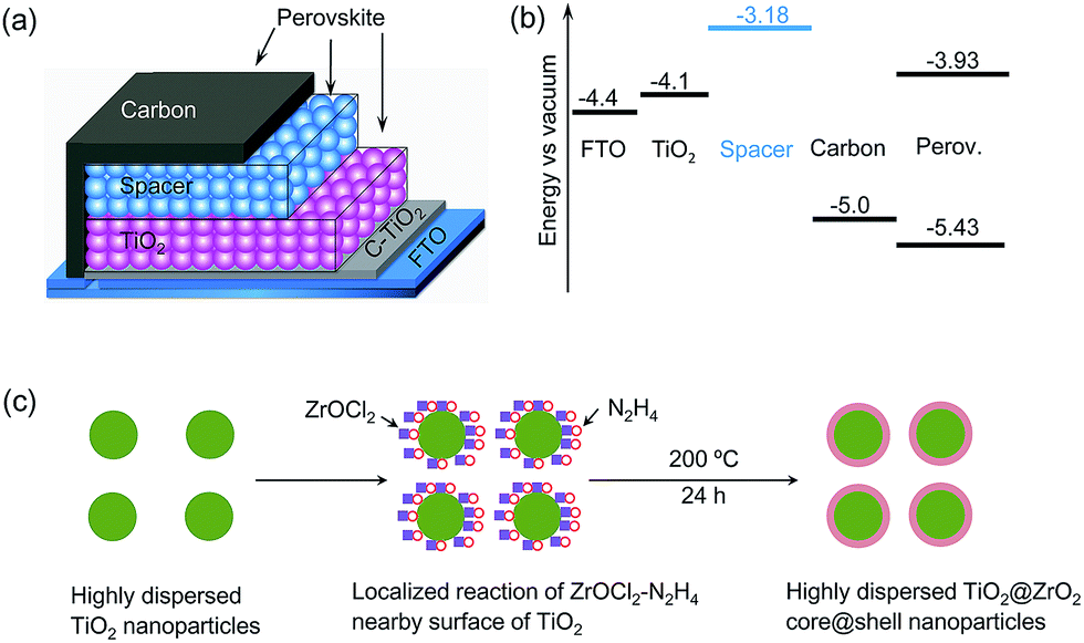 | ||
| Fig. 1 (a) Structure of TSC films based perovskite device and (b) energy levels of main components in device. (c) Synthesis route of TiO2@ZrO2 nanoparticles. | ||
Fig. 1c shows the chemical route to synthesize highly dispersible TiO2@ZrO2 core@shell (abbreviated as T@Z) nanoparticles to obtain spacer paste. First, highly dispersible TiO2 nanoparticles as the template are synthesized by hydrothermal method previously reported.45 Second, T@Z core@shell nanoparticles are synthesized. N2H4 coordinate with Zr4+ ion firstly. After the reaction of localized ZrOCl2–N2H4 complex, ZrO2 heterogeneously grow on TiO2 nanoparticles. ZrOCl2–N2H4 complex can produce homogeneous small-sized nanoparticles because of passivation effect during nucleation and growth stages.46
Fig. 2a shows XRD patterns of T@Z nanoparticles. Diffraction peaks at 2θ of 25.2°, 36.9°, 37.7°, 38.6°, 48° are in agreement with that of anatase TiO2 (JCPDS 21-1272). Peaks at 30.3° are assigned to plane (101) of tetragonal ZrO2 (JCPDS 79-1771) while 2θ of 28.2° and 31.5° are diffraction peaks of plane (−111) and (111) from monoclinic ZrO2 (JCPDS 01-0750). These XRD analysis proves that TiO2 crystals and ZrO2 crystals coexist, and ZrO2 nanoparticles are mixture of tetragonal phase and monoclinic phase, which is in agreement with the previous literature.46 However, main diffraction peak (28.2°) from plane (101) of TiO2 is slightly lower than standard location (28.3°), indicating that TiO2 lattice is slightly expanded due to possible substitution of titanium atom by zirconium atom during synthesis and subsequent sintering. The more broaden diffraction peaks belonging to ZrO2 compared to TiO2 indicates that ZrO2 has smaller size than TiO2. According to Scherrer equation, the sizes of nanocrystals are about 4 nm and 23.4 nm for ZrO2 and TiO2, respectively. High resolution TEM images (Fig. S1†) of T@Z nanoparticles further reveal that ca. 25 nm TiO2 nanoparticles are firmly surrounded by 5 nm ZrO2 nanoparticles, in which lattice fringes of both TiO2 and ZrO2 can be observed, which is consistent with XRD results. HAADF images of T@Z nanoparticles in Fig. 2c maps the location of element of Ti and Zr and further proved that TiO2 is covered by ZrO2 nanoparticles closely.
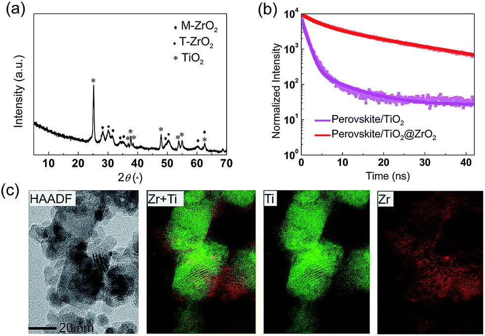 | ||
| Fig. 2 Characterizations of TiO2@ZrO2 spacer nanoparticles. (a) XRD of TiO2@ZrO2 spacer. (b) Time-resolved PL of perovskite/TiO2@ZrO2 spacer. (c) HAADF images of TiO2@ZrO2 spacer. | ||
The prerequisite of T@Z nanoparticles as spacer is that electrons in perovskite cannot flow into TiO2 encapsulated by ZrO2. In order to determine whether T@Z nanoparticles are compatible to act as spacer within the FP-MMPSC, we performed time-resolved photoluminescence measurement of the perovskite filled in T@Z, TiO2, as presented in Fig. 2b. PL decay time constant (12.2 ns) of perovskite/T@Z film is much longer than that (1.0 ns) of perovskite/TiO2, which evidences that in T@Z nanoparticles, ZrO2 sufficiently insulates perovskite from TiO2 growth template. The PL decay time constant of perovskite/T@Z spacer film is also very similar with that (13.6 ns) of perovskite/conventional spacer film (Fig. S2a†). From the Brunauer–Emmett–Teller (BET) test, the pore size of spacer films are 39 and 38 nm for T@Z and conventional spacer, respectively. The perovskite is confined in the mesopores of spacer. The average crystallite sizes of perovskite in both spacer are 20 nm calculated from XRD using the Scherrer equation (Fig. S2b†).
Morphology and insulating property of spacer
The calculated surface areas from BET method are 54 and 26 m2 g−1 for T@Z and conventional spacer, respectively. The much larger surface areas of T@Z than conventional spacer are attributed to smaller size of 5 nm-ZrO2. The top-view SEM images (Fig. 3a and b) highlight the considerable differences between the T@Z spacer and conventional spacer film morphology. For 5 nm ZrO2 alone, ZrO2 film has cracks due to the shrinkage during sintering (Fig. S3†) but there are no aggregates. The T@Z film not only contains no aggregates but also is very uniform over a large area. On the other hand, conventional spacer film shows the cracks and large aggregates (1–2 μm, Fig. 3b). The T@Z spacer film (Fig. 3c) is very flat with thickness of about 1 μm and the root mean square (rms) roughness value of 20.3 nm. In contrast, the conventional film (Fig. 3d) has an undulating nature, with film thickness varying from 0.2 to 2.5 μm and rms roughness of 203.9 nm, so it is possible to have direct contact between carbon film and TiO2 in very thin area. The surface morphology was also reflected in surface-profiles (Fig. S4†). The T@Z film was much more flat compared with that of conventional film. The flatness of T@Z film reflects the homogeneous dispersion of building blocks in paste and the roughness of conventional film reflects the aggregations.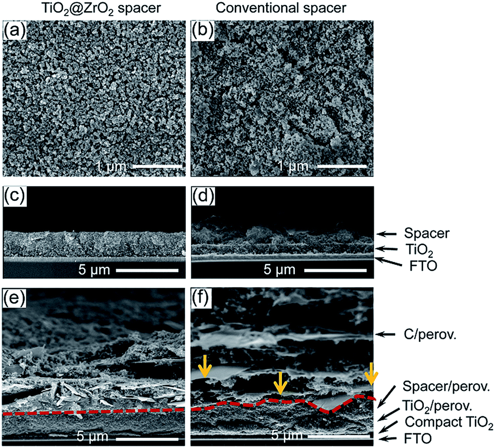 | ||
| Fig. 3 SEM images of spacer, interface morphology of devices based on different spacer. SEM top views of a T@Z spacer (a) and a conventional spacer (b). Cross-sectional SEM images of a T@Z spacer (c) and a conventional spacer (d). Cross-sectional SEM images of completed solar cells constructed from a T@Z spacer (e) and a conventional spacer (f). | ||
A setup in Fig. S5† was designed to measure the insulating property of spacer film. The resistance between carbon electrode and FTO electrode (here called ‘insulating resistance’, RI) reflects the insulating ability of spacer film. In an ideal condition, the insulating resistance should be infinite. However, the measured value of insulating resistance is finite, due to the direct contact between carbon and FTO electrode. The resistance (1.79 kΩ) in case of T@Z spacer is larger than that (0.96 kΩ) of conventional spacer indicates that T@Z spacer can prevent carbon film from contacting with substrate more efficiently than conventional spacer. It is reasonably to be expected that the separating resistance can reflect the separating property of spacer sandwiched between TiO2 and carbon layer.
The different insulating ability is resulted from two aspects. First, the flat and crack-free T@Z spacer has reduced probability of direct contact of carbon electrode and the substrate than undulated and crack conventional spacer. Second, quantum size effect of 5 nm-ZrO2 has low temperature sintering property. The T@Z spacer will sinter better than conventional spacer with the same nanoparticle dimensions at the same sintering temperature.
Fig. 3e and f shows that the morphology of spacer strongly affects the interface contacts of spacer/carbon in the cross sections of devices after infiltration of perovskite in mesopores of carbon, spacer and TiO2. Thus, from Fig. 3e, the interface between carbon/perovskite composite and T@Z/perovskite composite is very flat and compact over long range, resulting from flat T@Z spacer. In contrast, the interface between carbon/perovskite composite and conventional spacer/perovskite composite is uneven and gaps with width of over 500 nm exist, marked by yellow arrows in Fig. 3f. The discontinuous interface contact is resulted from undulated spacer in Fig. 3d. The border line between TiO2 and spacer film is blurred due to filling pores with perovskite. High resolution SEM images of zones close to FTO substrate indicates that full filling of pores in P25 film through carbon film and spacer layer were achieved in both devices (Fig. S6†). The color of both devices looks black, which is the same with our previous observations.27 5 nm-ZrO2 based device is poorly filled by (5-AVA)xMA1−xPbI3 and color of device looks light red brown due to too small pores. In previous study, it was shown that high pore filling is necessary for high performance device.26,47 So the 5 nm ZrO2 film is not considered for further device optimization.
Photovoltaic data of perovskite solar cells with different spacer
According to previous study, small illumination area of less than 0.1 cm2 will exaggerate PCE.48 Therefore, we employed illumination area of 0.13 cm2 to obtain reliable PCE. The typical current-density versus voltage (current–voltage) curves measured under simulated AM1.5G illumination for T@Z and conventional spacer based solar cells are shown in Fig. 4a. The photovoltaic parameters of these devices are summarized in Table 1 (and Fig. S7†). In all cases, the average thickness of spacer layer is 1.0 μm.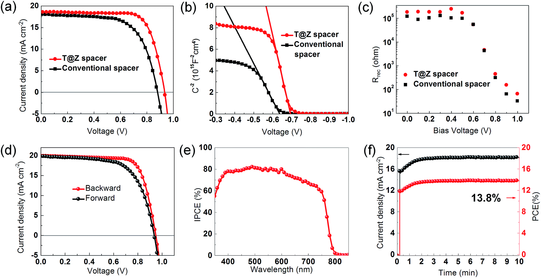 | ||
| Fig. 4 Photovoltaic performance of solar cells based on different spacer films. J–V (a) of the devices with T@Z spacer and conventional spacer. Mott–Schottky analysis (b) and impedance spectroscopy recombination resistance (c) at different bias for the devices with T@Z spacer and conventional spacer. (d) J–V curve of the best cell. (e) The corresponding IPCE spectrum (red). (f) Stabilized photocurrent output of the perovskite device with T@Z spacer biased at 0.76 V under simulated 1 sun illumination. | ||
| Spacer | RI (kΩ) | Voc (mV) | Jsc (mA cm−2) | FF | PCE (%) |
|---|---|---|---|---|---|
| T@Z | 1.77 | 935 | 18.6 | 0.73 | 12.5 |
| Conventional | 0.97 | 879 | 18.0 | 0.65 | 10.2 |
The device based on conventional spacer gave an average open-circuit voltage (Voc) of 0.879 V, a short-circuit photocurrent (Jsc) of 18.0 mA cm−2, a fill factor (FF) of 0.65, reaching a PCE of 10.2%. In contrast, the cell fabricated with T@Z exhibited significantly enhanced PCE of 12.5% with an average Voc of 0.935 V, a Jsc of 18.6 mA cm−2, and a FF of 0.73. From statistic data of two series of photovoltaic data presented in Fig. S7a–d,† Voc and FF of flat T@Z spacer based devices are significantly enhanced compared to undulated conventional spacer based device. The improved performance is a result of the flat and compact interface contact between carbon electrode and perovskite layer confined in spacer, along with reduced probability of direct contact between carbon and TiO2.
To further clarify the improvement of Voc and FF, Mott–Schottky analysis and impedance spectra analysis of devices based on different spacer were conducted (Fig. 4b and c). From the X-intercept of the linear regime in the Mott–Schottky plot (Fig. 4b), the built-in potential at the TiO2/(5-AVA)xMA1−xPbI3 contact can be obtained.36,37 The built-in potential of the device based on flat T@Z spacer is around 58 mV higher than that of the device based on conventional spacer. The recombination resistance of device based on flat T@Z spacer is also larger than that of the device based on conventional spacer, indicating that solar cell with T@Z spacer has less recombination probability than conventional spacer. These differences should be attributed to decreased electrons combination from TiO2 to carbon electrode and are responsible for performance enhancement. When flat mesoporous TiO2 film with thickness of 1 μm is inserted between carbon layer and TiO2 layer, much lower PCE is obtained because of very low Voc (597 mV) (Table S1†). The decreased Voc is resulted from severe recombination caused by charge transfer from the conduction band of TiO2 to carbon electrode directly. This substantially improved Voc by employing insulating film as spacer layer clarified the importance of insulating property of spacer film. These results emphasized the critical role of the quality of spacer film, including morphology and insulating property, in order to realize ultimate high efficiency in this type of mesoscopic perovskite solar cell.
Thickness of T@Z spacer was tuned to optimize performance of device and parameters are presented in Fig. S8.† Device with 1 μm thick T@Z spacer performed the best in average. Hysteresis in the J–V curves of perovskite solar cells dependent on the direction of scan has been observed.49 To further ensure the reliability of efficiency of best-performing device, the champion device was scanned forward and backward, and its stabilized Pmax was also recorded, which are shown in Fig. 4d and e and parameters are summarized in Table 2. When scanned backward, PCE of 13.7% is obtained, with Jsc, Voc, and FF of 19.91 mA cm−2, 0.948 V, 0.73, respectively. Meanwhile, when scanned forward, PCE of 12.0% is obtained, with Jsc, Voc, and FF of 19.82 mA cm−2, 0.935 V, 0.65, respectively. There is only little difference in Jsc and Voc between forward and backward scanning. The Jsc integrating from IPCE spectra is 18.5 mA cm−2, which is 10% smaller than value obtained by J–V curve due to a slow response of photocurrent. The steady output photocurrent density when biased at 0.76 V was 18.2 mA cm−2, leading to a steady output power of 13.8%, which matches well with the value obtained from backward scan J–V curve. It is commonly accepted that steady output power is more real than averaged value from forward scanning and backward scanning.49,50 In addition, device based on T@Z spacer film own very stable light soaking stability (Fig. S9†). Under continuous AM1.5G simulated sunlight with no UV light cut-off filter inserted between light source and solar cell, performance of device did not change after 40 hours in ambient atmosphere without encapsulation.
| Condition | Voc (mV) | Jsc (mA cm−2) | FF | PCE (%) |
|---|---|---|---|---|
| Forward | 0.935 | 19.82 | 0.65 | 12.0 |
| Backward | 0.948 | 19.91 | 0.73 | 13.7 |
| Average | 0.942 | 19.87 | 0.69 | 12.9 |
| Stabilized | 13.8 |
Conclusions
In summary, highly dispersible TiO2@ZrO2 nanoparticles were synthesized as building blocks for flat and uniform spacer in fully printable mesoscopic perovskite solar cell. Results from SEM cross-sectional images of devices, J–V curves, impedance spectra, and Mott–Schottky analysis revealed that flat and crack-free spacer is preferred for achieving better separating property and creating flat and defect-free interface between carbon electrode and perovskite layer confined in spacer film. The separating property is critical to efficiently separate carbon from TiO2, avoid recombination of electrons from electron transporting materials to carbon electrode, and harvest light uniformly. The flat and defect-free interface between carbon electrode and perovskite layer is beneficial to collect holes efficiently for carbon electrode. When the designed film through screen printing is employed as spacer, steady output power conversion efficiency of 13.8% is obtained. Moreover, flat spacer makes it possible to very precisely tune thickness of perovskite hosted in spacer layer. More advanced spacer preparation method will further improve the efficiency. Combination with superior light soaking stability without encapsulation or UV light cut-off filter, and low cost of raw materials, such as commercial Degussa P25, graphite and carbon black, our results stands for one important step of approaching commercialization of perovskite-based solar cell.Acknowledgements
Thanks for helpful discussion with Dr Xinhua Zhong. The authors acknowledge the financial support by the Ministry of Science and Technology of China (863, No. SS2013AA50303), the National Natural Science Foundation of China (Grant No. 61106056) and Scientific Research Foundation for Returned Scholars, Ministry of Education of China. We also thank the Analytical and Testing Center of Huazhong University of Science and Technology (HUST) for scanning electron microscopy (SEM), field emission scanning electron microscopy (FE-SEM), field emission transmission electron microscopy (FTEM) and X-ray diffraction (XRD) testing.Notes and references
- C. Bi, Q. Wang, Y. Shao, Y. Yuan, Z. Xiao and J. Huang, Nat. Commun., 2015, 6, 1–7 Search PubMed.
- Q. Dong, Y. Fang, Y. Shao, P. Mulligan, J. Qiu, L. Cao and J. Huang, Science, 2015, 347, 967–970 CrossRef CAS PubMed.
- F. Hao, C. C. Stoumpos, R. P. Chang and M. G. Kanatzidis, J. Am. Chem. Soc., 2014, 136, 8094–8099 CrossRef CAS PubMed.
- N. Kitazawa, Y. Watanabe and Y. Nakamura, J. Mater. Sci., 2002, 37, 3585–3587 CrossRef CAS.
- A. Kojima, K. Teshima, Y. Shirai and T. Miyasaka, J. Am. Chem. Soc., 2009, 131, 6050–6051 CrossRef CAS PubMed.
- W. J. Yin, T. Shi and Y. Yan, Adv. Mater., 2014, 26, 4653–4658 CrossRef CAS PubMed.
- W.-J. Yin, T. Shi and Y. Yan, Appl. Phys. Lett., 2014, 104, 1–4 Search PubMed.
- H. Shi and M.-H. Du, Phys. Rev. B: Condens. Matter Mater. Phys., 2014, 90, 1–6 Search PubMed.
- J. W. Jung, C.-C. Chueh and A. K.-Y. Jen, Adv. Mater., 2015, 27, 7874–7880 CrossRef CAS PubMed.
- J. H. Kim, S. T. Williams, N. Cho, C.-C. Chueh and A. K.-Y. Jen, Adv. Energy Mater., 2015, 5, 1–6 Search PubMed.
- Q. Chen, H. Zhou, Z. Hong, S. Luo, H.-S. Duan, H.-H. Wang, Y. Liu, G. Li and Y. Yang, J. Am. Chem. Soc., 2014, 136, 622–625 CrossRef CAS PubMed.
- J. Chen, Y. Rong, A. Mei, Y. Xiong, T. Liu, Y. Sheng, P. Jiang, L. Hong, Y. Guan, X. Zhu, X. Hou, M. Duan, J. Zhao, X. Li and H. Han, Adv. Energy Mater., 2015, 1502009, 1–6 Search PubMed.
- H. Azimi, T. Ameri, H. Zhang, Y. Hou, C. O. R. Quiroz, J. Min, M. Y. Hu, Z. G. Zhang, T. Przybilla, G. J. Matt, E. Spiecker, Y. F. Li and C. J. Brabec, Adv. Energy Mater., 2015, 5, 1–6 Search PubMed.
- K.-G. Lim, H.-B. Kim, J. Jeong, H. Kim, J. Y. Kim and T.-W. Lee, Adv. Mater., 2014, 26, 6461–6466 CrossRef CAS PubMed.
- H. Zhou, Q. Chen, G. Li, S. Luo, T.-b. Song, H.-S. Duan, Z. Hong, J. You, Y. Liu and Y. Yang, Science, 2014, 345, 542–546 CrossRef CAS PubMed.
- N. J. Jeon, J. H. Noh, Y. C. Kim, W. S. Yang, S. Ryu and S. I. Seok, Nat. Mater., 2014, 13, 897–903 CrossRef CAS PubMed.
- M. Liu, M. B. Johnston and H. J. Snaith, Nature, 2013, 501, 395–398 CrossRef CAS PubMed.
- W. Nie, H. Tsai, R. Asadpour, J.-C. Blancon, A. J. Neukirch, J. J. C. Gautam Gupta, M. Chhowalla, S. Tretiak, M. A. Alam, H.-L. Wang and A. D. Mohite, Science, 2015, 347, 522–525 CrossRef CAS PubMed.
- Z. Xiao, Q. Dong, C. Bi, Y. Shao, Y. Yuan and J. Huang, Adv. Mater., 2014, 26, 6503–6509 CrossRef CAS PubMed.
- W. S. Yang, J. H. Noh, N. J. Jeon, Y. C. Kim, S. Ryu, J. Seo and S. I. Seok, Science, 2015, 348, 1234–1237 CrossRef CAS PubMed.
- J. Burschka, N. Pellet, S. J. Moon, R. Humphry-Baker, P. Gao, M. K. Nazeeruddin and M. Gratzel, Nature, 2013, 499, 316–319 CrossRef CAS PubMed.
- X. Li, M. I. Dar, C. Yi, M. K. Nazeeruddin, J. Luo, H. Han and M. Grätzel, Nat. Chem., 2015, 7, 703–711 CrossRef CAS PubMed.
- X. Li, D. Bi, C. Yi, J. Décoppet, J. Luo, S. M. Zakeeruddin, A. Hagfeldt and M. Grätzel, Science, 2016, 353, 58–62 CrossRef CAS PubMed.
- http://www.nrel.gov/ncpv/images/efficiency_chart.jpg.
- Z. Ku, Y. Rong, M. Xu, T. Liu and H. Han, Sci. Rep., 2013, 3, 1–5 Search PubMed.
- T. Liu, L. Liu, M. Hu, Y. Yang, L. Zhang, A. Mei and H. Han, J. Power Sources, 2015, 293, 533–538 CrossRef CAS.
- A. Mei, X. Li, L. Liu, Z. Ku, T. Liu, Y. Rong, M. Xu, M. Hu, J. Chen, Y. Yang, M. Gratzel and H. Han, Science, 2014, 345, 295–298 CrossRef CAS PubMed.
- L. Liu, A. Mei, T. Liu, P. Jiang, Y. Sheng, L. Zhang and H. Han, J. Am. Chem. Soc., 2015, 137, 1790–1793 CrossRef CAS PubMed.
- X. Li, M. Tschumi, H. Han, S. S. Babkair, R. A. Alzubaydi, A. A. Ansari, S. S. Habib, M. K. Nazeeruddin, S. M. Zakeeruddin and M. Grätzel, Energy Technol., 2015, 3, 551–555 CrossRef CAS.
- L. Etgar, P. Gao, Z. Xue, Q. Peng, A. K. Chandiran, B. Liu, M. K. Nazeeruddin and M. Gratzel, J. Am. Chem. Soc., 2012, 134, 17396–17399 CrossRef CAS PubMed.
- H. Wei, J. Xiao, Y. Yang, S. Lv, J. Shi, J. D. Xin Xu, D. L. Yanhong Luo and Q. Meng, Carbon, 2015, 93, 861–868 CrossRef CAS.
- Y. Yang, J. Xiao, H. Wei, L. Zhu, D. Li, Y. Luo, H. Wu and Q. Meng, RSC Adv., 2014, 4, 52825–52830 RSC.
- H. Chen, Z. Wei, H. He, X. Zheng, K. S. Wong and S. Yang, Adv. Energy Mater., 2016, 1502087, 1–10 Search PubMed.
- Z. Wei, H. Chen, K. Yan and S. Yang, Angew. Chem., Int. Ed., 2014, 53, 13239–13243 CrossRef CAS PubMed.
- Z. Zhu, J. Ma, Z. Wang, C. Mu, Z. Fan, L. Du, Y. Bai, L. Fan, H. Yan, D. L. Phillips and S. Yang, J. Am. Chem. Soc., 2014, 136, 3760–3763 CrossRef CAS PubMed.
- W. A. Laban and L. Etgar, Energy Environ. Sci., 2013, 6, 3249–3253 CAS.
- A. Sigalit, G. Shany, C. B. El and E. Lioz, Phys. Chem. Chem. Phys., 2014, 16, 10512–10518 RSC.
- M. Hu, L. Liu, A. Mei, Y. Yang, T. Liu and H. Han, J. Mater. Chem. A, 2014, 2, 17115–17121 CAS.
- A. Mei, X. Li, L. Liu, Z. Ku, T. Liu, Y. Rong, M. Xu, M. Hu, J. Chen, Y. Yang, M. Graetzel and H. Han, Science, 2014, 345, 295–298 CrossRef CAS PubMed.
- Y. Rong, Z. Ku, A. Mei, T. Liu, M. Xu, S. Ko, X. Li and H. Han, J. Phys. Chem. Lett., 2014, 5, 2160–2164 CrossRef CAS PubMed.
- F. Hao, C. C. Stoumpos, Z. Liu, R. P. H. Chang and M. G. Kanatzidis, J. Am. Chem. Soc., 2014, 136, 16411–16419 CrossRef CAS PubMed.
- O. Vasylkiv and Y. Sakka, J. Am. Ceram. Soc., 2001, 84, 2489–2494 CrossRef CAS.
- K. Yan, Z. Wei, J. Li, H. Chen, Y. Yi, X. Zheng, X. Long, Z. Wang, J. Wang, J. Xu and S. Yang, Small, 2015, 11, 2269–2274 CrossRef CAS PubMed.
- Z. Wei, K. Yan, H. Chen, Y. Yi, T. Zhang, X. Long, J. Li, L. Zhang, J. Wang and S. Yang, Energy Environ. Sci., 2014, 7, 3326–3333 CAS.
- Y. Yang, K. Ri, A. Mei, L. Liu, M. Hu, T. Liu, X. Li and H. Han, J. Mater. Chem. A, 2015, 3, 9103–9107 CAS.
- H. Zhu, D. Yang, Z. Xi and L. Zhu, J. Am. Ceram. Soc., 2007, 90, 1334–1338 CrossRef CAS.
- T. Leijtens, B. Lauber, G. E. Eperon, S. D. Stranks and H. J. Snaith, J. Phys. Chem. Lett., 2014, 5, 1096–1102 CrossRef CAS PubMed.
- S. Ito, M. K. Nazeeruddin, P. Liska, P. Comte, R. Charvet, P. Péchy, M. Jirousek, A. Kay, S. M. Zakeeruddin and M. Grätzel, Prog. Photovoltaics, 2006, 14, 589–601 CAS.
- J. A. Christians, J. S. Manser and P. V. Kamat, J. Phys. Chem. Lett., 2015, 6, 852–857 CrossRef CAS PubMed.
- T. Leijtens, G. E. Eperon, N. K. Noel, S. N. Habisreutinger, A. Petrozza and H. J. Snaith, Adv. Energy Mater., 2015, 5, 1–23 Search PubMed.
Footnotes |
| † Electronic supplementary information (ESI) available: Experimental section, Fig. S1–S9: TEM of nanoparticles, time-resolved PL and XRD of perovskite/nanoparticles, SEM images of 5 nm ZrO2, roughness profiles of different spacer films setup designed to measure insulating properties of spacer. High resolution cross-section SEM of device, histogram of photovoltaic parameters and photo-stability of devices. See DOI: 10.1039/c6ra25347d |
| ‡ These authors contributed equally to this work. |
| This journal is © The Royal Society of Chemistry 2017 |