DOI:
10.1039/C6RA25233H
(Paper)
RSC Adv., 2017,
7, 771-781
Correlation between magnetic and micro-structural properties of low energy ion irradiated and un-irradiated Zn0.95Mn0.05O films†
Received
14th October 2016
, Accepted 22nd November 2016
First published on 3rd January 2017
Abstract
To establish intrinsic ferromagnetism (FM) and to detect its micro-structural origin (if any), sol–gel derived Zn0.95Mn0.05O films have been undergone low energy (800 keV) Ar4+ ion irradiation. The structural, optical, magnetic and micro-structural properties of irradiated and un-irradiated films were investigated by X-ray diffraction (XRD), UV-visible and photoluminescence (PL) spectroscopy, field and temperature dependent magnetization measurements, X-ray absorption near edge spectroscopy (XANES) and extended X-ray absorption fine structure (EXAFS) spectroscopy. All the films exhibit single-phase wurtzite structure and intrinsic FM. The band gap and band tail parameters show systematic variation with fluence of irradiation. PL spectra exhibit a green emission peak (oxygen vacancy) and that has been suppressed significantly for the film with low fluence (5 × 10¹⁴ ions per cm2) of irradiation. The film irradiated with low fluence exhibits an absence of antiferromagnetic (AFM) interaction and the strongest FM. The studies of XANES and EXAFS indicate a difference in oxidation state and local environment for Mn in comparison to Zn in the host ZnO matrix. The film that exhibits strong FM also shows a comparatively higher number of tetrahedral coordinated Mn ions. The magnetic properties have been correlated with optical and micro-structural properties and low fluence of ion irradiation has been supposed to be optimized.
Introduction
Dilute magnetic semiconductors (DMS) are promising materials for spintronics as they exploit the intrinsic spin degree of freedom of electrons in addition to charge degree of freedom. Room temperature (RT) FM was reported in wide band gap semiconductors such as GaN and ZnO.1–3 There are many theoretical4,5 and experimental6–8 studies on DMS in which very few cations are substituted with transition metal (TM) ions to develop intrinsic FM above RT. So far as spintronic application is concerned the study on nanostructured TM doped ZnO thin films is more useful than nanoparticles as thin films of TM doped ZnO have further interesting utilities such as high transparency and conductivity9 apart from intrinsic FM above RT.10 However, an undesirable phase segregation may occur and constitutes a problem in the TM doped DMS. Moreover, TM oxide inclusions may be ferromagnetic themselves; giving rise to doubts on the origin of FM in TM doped ZnO and causing complications for the growth of practical DMS materials. It can be resolved through local structural investigation. Hence, in this aspect, the charge state and coordination environment of TM ions in the host ZnO matrix is essentially an important issue. Further the origin of magnetism in TM (particularly Mn) doped ZnO was not understood completely. There was a time when several conflicting observations and reports regarding magnetic properties of TM doped ZnO based DMS actually posed a serious challenge. However, the researchers are successfully overcoming it with emergence of a general consensus that defects play a crucial role in controlling the magnetic properties of such systems.11–15
In terms of ferromagnetic interaction models, the most widely accepted model for interpreting intrinsic FM in TM doped ZnO is carrier (and nowadays defects) induced bound magnetic polaron (BMP) model.16 The noteworthy fact is that in case of Co doped ZnO, n-type carriers induced BMP drives the system towards ferromagnetic16 whereas p-type carrier induced BMP plays the same role for Mn doped ZnO.17 However, in absence of any donor or acceptor types of impurities in ZnO, point defects such as neutral or singly ionized zinc interstitial (ZnI), oxygen vacancy (VO) and zinc vacancy (VZn) can act as agents for developing BMP for Co and Mn doped ZnO and which in turn generate intrinsic FM.18
The issue of incorporation of defects into TM doped ZnO matrix can be manifested by ion irradiation/implantation. Energetic ions after entering into the target lose their energies mainly by collisions with (inelastic/elastic) atomic electrons. In this process when the ions move deeper inside the target, their velocities reduce and suffer a series of elastic collisions with the target atom's nuclei. Consequently, along the trajectory of the beam, a trail of defects such as point defects, defect clusters; structural phase formation etc. may be formed. The type of formation depends on the type of ions, its energy as well as the physical properties of the material. The radiation damage is developed in the neighborhood of the path of the ion beam. Neogi et al.19 observed metal insulator transition in 50 MeV Li3+ irradiated 2 at% Mn doped ZnO nanoparticles and interpreted this metal semiconductor transition due to creation of donor types of defects (oxygen vacancy). Ion beam irradiation can improve the structural property of the ZnO nanoparticles by dissolving the impurity phase,19 hence substitutional incorporation of Mn2+ at Zn2+ site (MnZn) and ferromagnetic property of the samples get improved.20 A close correlation between FM, defects and MnZn was evolved for 50 MeV Li3+ irradiated 4 at% Mn doped ZnO.20 Low energy ion irradiation using non-magnetic inert ions such Xe or Ar are useful to induce, organize and manipulate defects in the host material in a controlled fashion, to avoid segregation of nano-dimensional TM or its oxide clusters and to eliminate the complexities arising from the chemical reactivity of the ion beams.18,21
The interaction in Mn-doped ZnO was sometimes AFM due to contributions from both Mn ions with Mn nearest neighbors and from isolated spins.22 Actually, the coordination environment of Mn ions in ZnO affects its magnetic properties. It is important to identify the coordination environment of Mn in order to interpret the origin of magnetism. However, it is difficult to characterize the coordination environment of a dopant, especially in a diluted content. EXAFS is very sensitive to the local environment of a selected atom.23–25 The solubility of Mn in a ZnO lattice is low (less than 4 at%). Mn ions either go to the substitutional sites in the ZnO lattice forming Mn2+O4 tetrahedron or go to interstitial sites and forming Mn3+O6 octahedron.26 In order to investigate the oxidation state and occupation sites of the Mn ions in ZnO-based DMSs, XANES study seems to be necessary.
In this paper, structural, optical, magnetic and micro-structural properties of low energy Ar4+ irradiated sol–gel derived Zn0.95Mn0.05O films were analyzed. All single-phase wurtzite nanostructured films exhibit a non-monotonous variation of FM with fluence of irradiations. This variation has been nicely correlated with MnZn and interstitial Mn as evidenced from XAS measurement. FM of the thin films has been interpreted assuming formation of BMPs. All these films show transmittance around 90% thereby exhibiting strong potential for transparent electrode application apart from their desired spin electronic application.
Experimental section
Zn0.95Mn0.05O films were synthesized by sol–gel spin coating technique. Appropriate amount of zinc acetate [Zn(CH3COO)2·2H2O] and manganese acetate [Mn(CH3COO)2·2H2O] was added to a solution containing 2-propanol and di-ethanolamine (DEA). DEA was used to stabilize the solution. The solution was used for spin coating on the glass substrates to synthesize the films. The spinning rate and period were optimized to 2000 rpm and 35 s, respectively. After coating, the films were dried at 300 °C for 15 minutes to evaporate the solvent and finally it was heat treated at 500 °C to obtain good quality films.10,18 The process of coating and subsequent annealing was repeated for five times to obtain the desired film thickness. Rutherford Back Scattering (RBS) measurement was performed to estimate the thickness of the films and the average thickness of the films was estimated to be of 550 nm. The area of the target (films) was maintained at 1 cm2 same as the dimension of the Ar4+ beam. The films were irradiated by low energy (800 keV) Ar4+ beam. Different fluence (5 × 10¹⁴, 1015, 5 × 10¹⁵ and 1016 ions per cm2) was chosen for irradiation. The irradiation fluence ‘F’ (ions per cm2) has been estimated by using the following relation:| |
 | (1) |
here Ip represents the ion current, T is the total time for a particular sample to be irradiated, e is the electronic charge (1.6 × 10⁻¹⁹ C), n is the charge state of the impinging ions and A is area of the ion beam. While irradiating the samples the beam current was chosen as Ip = 2 μA or 1 μA, to increase the time for a particular fluence so that the error in time counting can be minimized. Irradiation experiment was carried out in a high vacuum chamber at room temperature. During irradiation the sample temperature is kept at 300 K. Also penetration depths of different Ar4+ beams are same, only fluences of irradiations are different for different films. The effect of ion irradiation on different physical properties (structural, optical and magnetic) of Zn0.95Mn0.05O films has been discussed as a function of fluence of irradiations. No post annealing treatment has been performed after irradiation for recovery of the irradiation-induced damages. The XRD patterns of the films were recorded with wavelength of X-ray as 1 Å. Field Effect Scanning Electron Micrographs (FESEM) was taken from the FEG, QUANTA-200 instrument. UV-visible spectra were recorded using a spectrophotometer (Perkin Elmer; model: Lambda 35) in the wavelength range (200–1100 nm). The Spectra were recorded by taking a similar glass as the reference so that transmission due to films only was obtained. PL spectra of the films at RT were recorded by using an excitation source of 325 nm line of He–Cd laser with an output power (∼10 mW). Magnetic measurements of the un-irradiated and irradiated films were performed in a SQUID VSM (Quantum Design). Magnetization against field M(H) at fixed temperature and magnetization against temperature M(T) at a given field (150 Oe) were measured. M(T) data was measured under zero field cooled (ZFC) and field cooled (FC) mode in the temperature range 5 K to 300 K. In order to explore the local structure of doping element (Mn), XAS (both XANES and EXAFS) at the Mn-K and Zn-K edges of the un-irradiated and a few selected irradiated films were carried out at room temperature in the fluorescence mode.27
Results and discussion
The penetration depth of Ar4+ ions is greater than the film thickness (∼550 nm). Considering the trajectory of the ions, electronic energy loss (Se) largely predominates over nuclear energy loss (Sn). The energy transfer through Sn can only knock out the target atoms from their lattice positions and creates stable vacancy or vacancy clusters. However, Se is mostly responsible for exciting the electrons of target atom. Se for the Ar4+ beam is far less than the critical value responsible for generation of point defects or correlated defect clusters. The stopping power and ranges of ion in matter (SRIM) calculation reveals that Ar4+ beam creates more damage at the Zn sites than O sites. However, SRIM only predicts about the generated displacements. Majority of such defects immediately faces annihilation (dynamic recovery) and that seems to be the origin of radiation hardness of ZnO.19 A detailed discussion in this aspect has been made in ESI.†
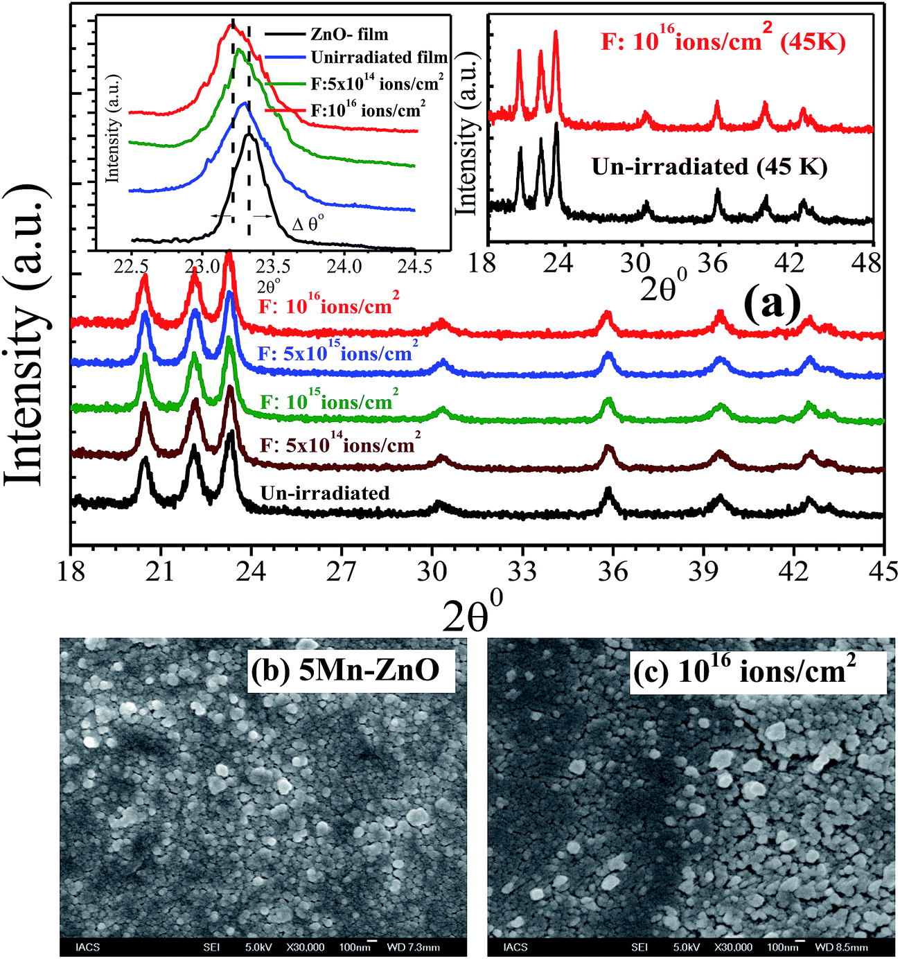
XRD patterns of the films at RT are represented in Fig. 1. XRD patterns reveal that the films are polycrystalline maintaining hexagonal wurtzite structure of ZnO. No additional diffraction peak(s) related to any Mn related oxide phase(s) has been observed. Left inset of Fig. 2 shows the expanded view of (101) peak of ZnO and Mn doped ZnO films. A slight low angle shifting of the (101) peak (from 2θ = 23.327° for ZnO to 2θ = 23.294° for Zn0.95Mn0.05O) has been noticed in Zn0.95Mn0.05O film. A small shift in the peak positions has not been observed after irradiation except for the film irradiated with fluence 1016 ions per cm2. Right inset of Fig. 2 shows XRD patterns for un-irradiated and irradiated film with fluence 1016 ions per cm2 at low temperature 45 K. The identical nature of these (45 K) patterns in comparison to patterns at RT indicates no structural change has taken place in the temperature range 45 K to 300 K. Lattice parameters a and c of respective films were calculated using the following relation and presented in Table 1.
| |
 | (2) |
here,
dhkl is the distance between the crystalline planes with indices (
h k l) and it was estimated using equation.
28| |
λ = 2dhkl![[thin space (1/6-em)]](https://www.rsc.org/images/entities/char_2009.gif) sinθ sinθ
| (3) |
 |
| | Fig. 1 (a) XRD patterns of all un-irradiated and irradiated Mn doped ZnO films; left inset: (101) peak of ZnO and other Mn doped ZnO films; right inset: XRD patterns of un-irradiated and irradiated film with fluence 1016 ions per cm2 films taken at 45 K. SEM patterns of (b) un-irradiated and (c) irradiated (fluence 1016 ions per cm2) films respectively. | |
 |
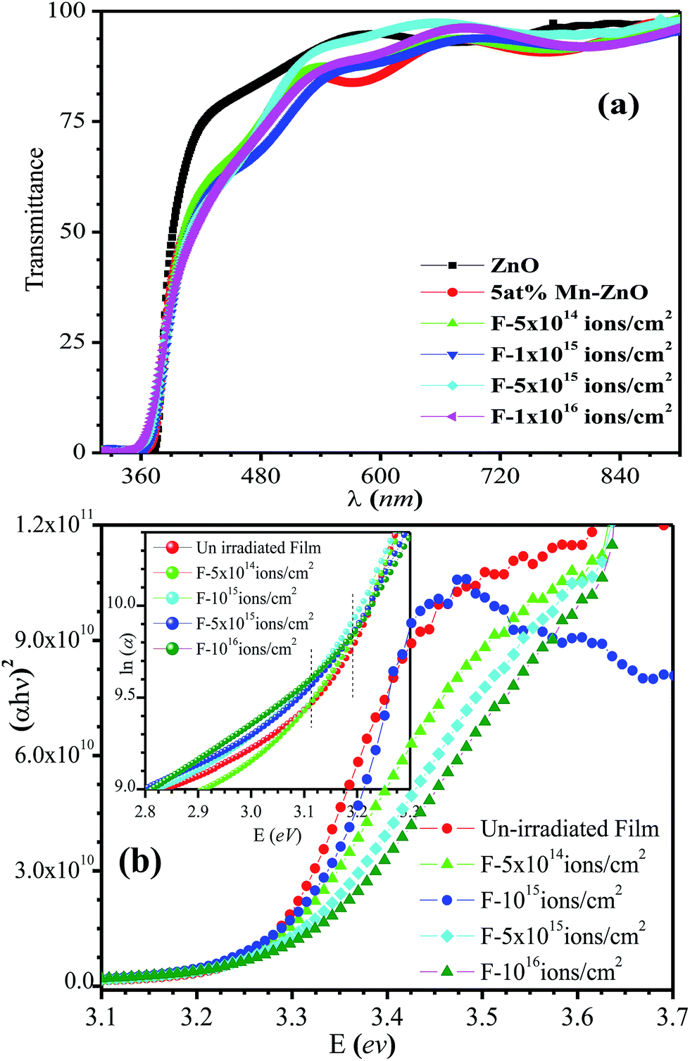
| | Fig. 2 (a) Variation of transmittance against wavelength of un-irradiated and irradiated films (b) variation of (αhν)2 against photon energy of the respective films, inset of (b) exhibits variation of ln(α) against photon energy of the respective films. | |
Table 1 Structural parameters (lattice constants), strain and grain size estimated from powder X-ray diffraction pattern
| Fluence (ions per cm2) |
a (Å) |
c (Å) |
c/a |
Strain |
Grain size from (101) peak (nm) |
Grain size (from W–H) (nm) |
| Un-irradiated |
3.244 |
5.217 |
1.608 |
5.95 × 10⁻³ |
14.30541 |
15.873 |
| 5 × 10¹⁴ |
3.251 |
5.203 |
1.600 |
11.06 × 10⁻³ |
15.10101 |
22.222 |
| 1 × 10¹⁵ |
3.251 |
5.217 |
1.605 |
13.26 × 10⁻³ |
15.75496 |
25.641 |
| 5 × 10¹⁵ |
3.248 |
5.208 |
1.603 |
13 × 10−3 |
15.06163 |
23.809 |
| 1 × 10¹⁶ |
3.248 |
5.213 |
1.605 |
4.9 × 10⁻³ |
14.97231 |
16.129 |
The estimated values of the lattice constants are shown in Table 1. For un-doped ZnO film the calculated values of lattice constant are a = 3.246 Å and c = 5.200 Å, which is quite comparable with that of the reported values of the lattice parameter (a = 3.246 Å, c = 5.202 Å) of pure ZnO thin film.28,29 The lattice constants, however, increase to a = 3.249 Å and c = 5.217 Å for the Zn0.95Mn0.05O film. The lower angle shifting of (101) peak and simultaneously increase in lattice constants indicates effect of Mn substitution at the Zn site in ZnO lattice.20 The change in lattice parameters with fluence of irradiation has been observed and it may be either due to change in occupancy of Mn2+ atoms at Zn sites or due to grain surface disorder introduced with irradiation.7,30 The broadening in XRD line profile of Zn0.95Mn0.05O film, as shown in the left inset of Fig. 2 indicates reduction in average crystallite size and strain induced by doping.31 Average crystallite size (D) was estimated from Scherrer's formula.20 D was found to be 14.3 ± 2 nm for un-irradiated Zn0.95Mn0.05O film. The XRD line-broadening pattern of irradiated films shows almost identical nature, indicating that average particle size does not change significantly after irradiation. The values of D for the irradiated films were almost same (15 ± 2 nm). In case of polycrystalline materials having grain sizes in nanometer range, grain interiors are relatively defect free (or contain scattered small size point defects) and the grain boundaries consist of high density defect clusters. Such local distortion generates strain and it also contributes to the XRD peak broadening, known as strain induced broadening. Williamson–Hall (W–H) plot technique was used to calculate the variation of lattice strain in the films.20,31 The micro strain (η) has been estimated using following equation:
| |
 | (4) |
The micro strain parameter η = |ΔDhkl/Dhkl| is determined from the slope of fitted straight line of the βcosθ against sinθ curve. The intercept of the line on the βcosθ axis provides the particle size corresponding to zero strain. The broadening of (100), (002), (101), (102), (110), (103), (112) peaks were used for W–H plot. In eqn (4) the anisotropic strain was ignored.31 The values of strain are presented in Table 1. After irradiation (for fluence 5 × 10¹⁴, 1015, 5 × 10¹⁵ ions per cm2) strain increases from that of un-irradiated film but for the film irradiated with fluence of 1016 ions per cm2, strain decreases. However, magnitude of the strain is quite small and hence their effect on XRD peak broadening seems to be negligible. Another point can be emphasized here is that severe degradation in crystallinity has not been observed even after irradiation with highest fluence. In fact, changes in full width at half maxima (FWHM) of the (101) peak are insignificant after irradiation. Hence, the impact of low energy (800 keV) irradiation did not affect the crystalline quality of the films. FESEM micrographs of un-irradiated and irradiated film (fluence 1016 ions per cm2) have been depicted in Fig. 1b and c respectively and they indicate nearly same grain structure (size and shape).
UV-visible absorption spectroscopy was used to study the variation in band gap of Zn0.95Mn0.05O films. Fig. 2a represents the transmission spectra of the films. The films show high transmittance in the visible wavelength region and absorption edge was found near 380 nm. High transparency of the films enhances their potential for practical application as transparent electrodes. The optical absorption coefficient α(λ) was estimated from the value of transmittance and thickness of the films. Fig. 2b shows variation of (αhν)2 against photon energy (hν) and the energy band gap was obtained from this plot. The estimated direct optical band gaps of all films are listed in Table 2. The band gap gradually enhanced from 3.273 eV for un-irradiated film to 3.301 eV in case of irradiated film of fluence 1016 ions per cm2. The observed blue shift may be explained using Burstein-Moss effect.32 Enhanced absorption just below the band edge has been observed (∼2.7 eV to 3 eV) for all Mn doped ZnO films inset of Fig. 2b. It may indicate the formation of defect states due to Mn doping near the band edge. This is known as band tailing effect and commonly observed in doped nanocrystalline ZnO. Absorption coefficient below the band edge (E < Eg) should vary exponentially with absorbed photon energy (E).
| |
 | (5) |
here,
α0 is a constant and
E0 is the band tail parameter.
E0 was estimated from the reciprocal of the slope of the linear part of the ln(
α)
versus E curve (
E <
Eg) as shown in the inset of
Fig. 2b. Any defect or disorder in ZnO gives rise to localized energy levels or discrete states within the band gap. The band tail parameter
E0 qualitatively describes the width of the localized states in the band gap without mentioning their energy position.
E0 represents the bulk-defect as well as grain-boundary trap concentrations in polycrystalline semiconductors. However, it is impossible to separate out explicitly the contribution of each disorder effect.
33 An increase in
E0 (band tail parameter) with irradiation fluence was observed and presented in
Table 2.
Table 2 Parameters estimated from optical (band gap energy and band tail parameter estimated from UV-visible spectra) spectroscopy and magnetization (saturation magnetization and coercivity at 300 K, 250 K and 200 K) studies
| Fluence (ions per cm2) |
Optical parameters |
Magnetic parameters |
| 300 K |
250 K |
200 K |
| Eg (eV) |
Eo (meV) |
MS (emu g−1) |
HC (Oe) |
MS (emu g−1) |
HC (Oe) |
MS (emu g−1) |
HC (Oe) |
| Un-irradiated |
3.273 |
119.97 |
0.55 |
45.34 |
0.89 |
40.83 |
0.98 |
39.75 |
| 5 × 10¹⁴ |
3.274 |
142.13 |
0.97 |
139.83 |
1.06 |
147.62 |
1.08 |
169.23 |
| 1 × 10¹⁵ |
3.283 |
158.84 |
0.19 |
39.10 |
0.20 |
36.26 |
0.21 |
33.40 |
| 5 × 10¹⁵ |
3.287 |
176.26 |
0.31 |
26.89 |
0.35 |
21.64 |
0.36 |
20.27 |
| 1 × 10¹⁶ |
3.301 |
192.50 |
0.84 |
7.54 |
0.87 |
5.82 |
0.89 |
4.71 |
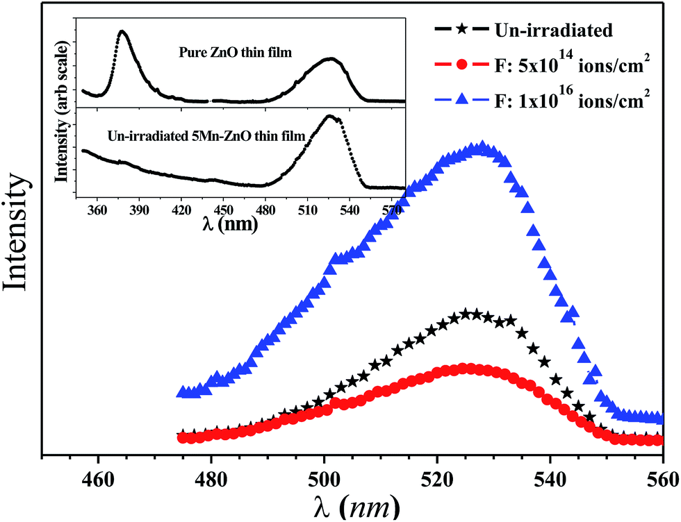
Fig. 3 shows the RT PL spectra of un-irradiated and irradiated Zn0.95Mn0.05O films. PL spectra of pure ZnO and un-irradiated Zn0.95Mn0.05O films have been presented in the inset. A prominent UV emission band (∼380 nm) and a broad visible emission band (450–550 nm) have been observed for pure ZnO film whereas UV emission band is absent in un-irradiated Zn0.95Mn0.05O film. UV emission originates due to recombination of free excitons whereas visible emission indicates presence of defects either vacancy types (VO, VZn) or interstitial types (OI, ZnI) in ZnO.34 It has been observed that Mn doping causes a large reduction in UV emission intensity.18 The reduction in emission intensity may be due to the increased non-radiative recombination processes with Mn doping.18 A broad green emission centered on 525 nm has been observed in the PL spectra of Zn0.95Mn0.05O thin films. Interestingly visible emission quenches at the low fluence (5 × 10¹⁴ ions per cm2), it increases and becomes comparable with un-irradiated Zn0.95Mn0.05O film at the intermediate fluence (5 × 10¹⁵ ions per cm2) and for highest fluence 1016 ions per cm2, intense visible luminescence was seen. The quenching of visible emission with irradiation fluence 5 × 10¹⁴ ions per cm2 is due to appearance of some non-radiative defect centers such as isolated VZn complexes.30 When fluence of irradiation increases, a saturation of defect concentrations is possible because spatial separation of VZn and ZnI decreases and ZnI recombines immediately with nearby VZn.30 Gradually free VZn concentration reduces with increasing fluence due to formation of complex VZn–ZnI pairs and simultaneously VO in higher proportions are generated. Green emission attributed to the recombination of electrons trapped in singly ionized oxygen vacancies (VO+) with photo generated holes35 is maximum for highest fluence (1016 ions per cm2) film indicating maximum concentration of VO+. A non-monotonous variation in intensity of visible emission indicates that their origin solely lies in the competition between defects generation and recovery during irradiation.
 |
| | Fig. 3 PL spectra of un-irradiated and irradiated (low and high fluence) Zn0.95Mn0.05O films. Inset: Shows PL spectra of ZnO and un-irradiated Zn0.95Mn0.05O films. | |
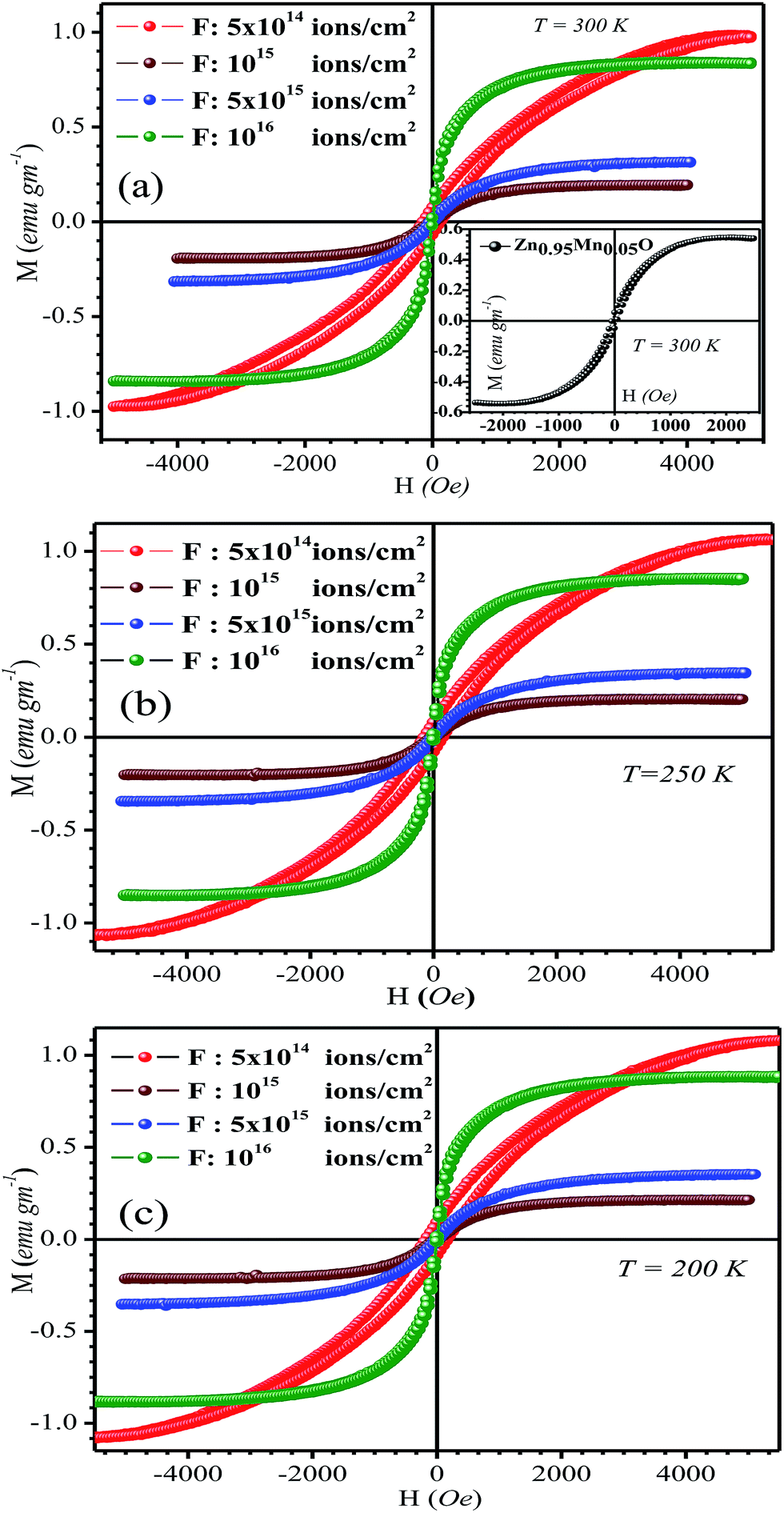
Fig. 4 represents M(H) variation of irradiated films at 300 K, 250 K and 200 K respectively. Inset of Fig. 4a depicts M(H) variation of un-irradiated film at 300 K. The M–H loop in low irradiation fluence (5 × 10¹⁴ ions per cm2) film is not well saturated with the given field whereas all other loops are well saturated. The saturation field seems to be quite larger for this particular film. This observation has been attributed to the requirement of substantially high saturation magnetic field to orient greater number of available spins in developing ferromagnetic exchange. The other films didn't require such high saturation magnetic field, as the number of involved spins for their ferromagnetic ordering is quite low. The saturation magnetization (MS) of the films was determined by subtracting diamagnetic contribution of glass substrate from the experimental data. The values of MS and coercivity (HC) are presented in Table 2. Un-irradiated film shows clear hysteresis at 300 K with MS = 0.55 emu g−1 and HC ∼50 Oe. After irradiation (fluence 5 × 10¹⁴ ions per cm2) ferromagnetic property of the film enhances, MS rises to 0.97 emu g−1 and HC ∼140 Oe. In fact this particular film shows highest magnetization among all films and comparatively large HC quite close to the reported result.18 Table 2 indicates diminishing value of MS at intermediate fluence. However, the film, irradiated with highest fluence (1016 ions per cm2) exhibits substantial MS (0.84 emu g−1) but low HC (10 Oe) at 300 K. The reports36,37 support this type of observed trend. With increasing fluence from 1015 to 1016 ions per cm2, MS gradually increases and HC gradually decreases. This trend is consistent with other report where variation of MS and HC show opposite trends indicating behavior like soft ferromagnet (strong reversibility).7 The nature of variation of MS and HC for all the irradiated films is identical at all measured temperatures viz. 300 K, 250 K and 200 K (Table 2), which, signifies steady and uniform magnetic properties of all films. 800 keV Ar ion irradiation actually imparts mainly a kind of electronic energy to the ZnO lattice. The increase of fluence indicates passage of energetic beam with increasing time only. Essentially with gradual increase of irradiation fluence the system was getting more and more homogeneous, so far as radiation damage is concerned. However, that does not have any simple correlation with orientation or randomization of available spins with increasing fluence of irradiation; rather a very complex correlation between irradiation fluence and MS seems to be operative. Conclusively, the process of irradiation with fixed energy on material like ZnO with minute amount of Mn doping and its dynamic recovery is extremely a complex process. Hence the system may response in a non-uniform manner so far as saturation magnetization is concerned though the variation can't alter the value of MS beyond the single order of magnitude. HC decreases for all irradiated films with decrease in temperature except for the film irradiated with lowest fluence. This type of anomalous temperature dependence of HC has been reported earlier38 and ascribed due to the anomalous temperature dependence of the magneto-crystalline anisotropy. The gradual increasing homogeneity (from the aspect of radiation damage) with gradual increase in irradiation fluence may actually monotonically decrease magneto-crystalline anisotropy and that is essentially reflected in gradual decreasing trend of HC at any fixed temperature with increase in irradiation fluence. The enhancement of magnetic properties of similar kind of oxides, viz. TiOx and NiO by annealing39,40 and ion beam bombardment41 in single or multilayers is worth mentioning. The CoPt and FePt thin films capped with ion-beam-assisted deposited TiOx in the annealed CoPt/TiOx39 and FePt/TiOx40 thin films exhibit strong enhancement in HC. The HC increased as the annealing temperature was raised, indicating more face center tetragonal-phase of CoPt and FePt were formed with higher annealing temperatures. The exchange bias effects of NiFe/NiO bilayers were studied by bombarding the bottom NiO surface with different ion-beam energies and durations.41 The enhancement in HC of NiFe/NiO bilayers is attributed to the changes in NiO anisotropies with different ion-beam bombardment durations on the NiO surfaces. The absolute values and enhancement of magnetic parameters in TiOx39,40 and NiO41 films are far more in comparison to the reported values in this work and it is primarily because of very diluted amount (5 at%) presence of magnetic ion (Mn).
 |
| | Fig. 4 The M(H) variation of irradiated Zn0.95Mn0.05O films (a) 300 K, (b) 250 K and (c) 200 K, respectively. Inset of (a) exhibit M(H) variation of un-irradiated Zn0.95Mn0.05O at 300 K. | |
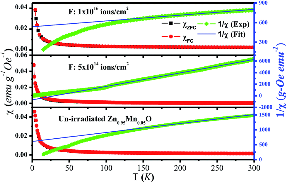
Magnetic susceptibility χ(T) curves have been presented in Fig. 5. The χ value was found to increase slowly with decreasing temperature from 300 K to about 80 K, and at low temperature (<80 K) there was a steep rise of χ with very strong concave curvature. The observed variation of χ(T) indicates existence of paramagnetic interaction that dominates at low temperature. Any distinct change in the χ(T) curves or magnetic phase transition has not been observed in the entire measured temperature range. The temperature dependent inverse magnetic susceptibility (χ−1) plot of the films at 300 Oe field and fit with Curie–Weiss law in the temperature range of 100–300 K was also presented in Fig. 5. In case of un-irradiated film, Currie–Weiss temperature (θ) comes out to be −202 K and for the irradiated film (fluence 1016 ions per cm2) θ is −605 K. Large negative values of θ indicate presence of antiferromagnetic (AFM) coupling between Mn ions. However, θ is found to be positive (30 K) for the low fluence irradiated film and in fact this film shows strongest FM. The suppression of FM due to AFM coupling is quite common for Mn doped ZnO,18,20 and evidenced here also excepting the low fluence irradiated film. The absence of AFM coupling in the low fluence Ar4+ ion irradiated Mn doped ZnO film is really a noteworthy phenomenon and it is one of the reasons for the film to be the strongest ferromagnet among all. Finally, the observed RT FM of all the films seems to be intrinsic as role of other factors have been nullified due to the following reasons: (i) no bifurcation have been found between ZFC and FC M(T) data with no signature of blocking temperature, ruling out the presence of spin-glass and/or superparamagnetic phases. (ii) The role of Mn oxide phases (below the detection limit of XRD) was eliminated, as none of these could be responsible for RT FM. Metallic Mn, MnO and MnO2 are all AFM below the Neel temperature of 100 K, 116 K and 84 K respectively and Mn3O4 is ferromagnetic with Currie temperature ∼45 K.37,42,43
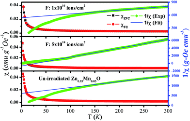 |
| | Fig. 5 Variation of magnetic susceptibility (left scale) and inverse of magnetic susceptibility (right scale) against temperature for un-irradiated and irradiated films with low and high fluence. | |
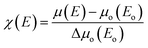
In order to probe the local atomic structure and occupation sites of Mn ions in ZnO, XAS of few selected films were performed. Fig. 6a represents the normalized Zn-K edge XANES spectra of un-irradiated and irradiated (fluence 1016 ions per cm2) Zn0.95Mn0.05O films. The XANES at Zn-K edge, measures electronic transitions from occupied Zn-1s to unoccupied Zn-4p states. For Zn2+ ions, the 3d orbital is completely filled; hence the pre edge signature like Mn-K edge is not expected. The A, B, and C, as highlighted in Fig. 6a are characteristic XANES peaks of wurtzite ZnO.44 These three peaks correspond to the electronic transitions from Zn-1s to Zn-4p along the c, a, and b axes of the unit cell of hexagonal ZnO. XANES pattern and edge positions of Zn-K edge for both these films are nearly identical and similar to the reported results.45,46 So, ion irradiation did not change much the oxidation state and local environment around Zn ions in these films. The analysis of EXAFS pattern was performed to study local electronic structures surrounding the absorbing ‘Zn’ atoms of respective films. The absorption coefficient ‘μ(E)’ has been converted into absorption function ‘χ(E)’ defined as follows:
| |
 | (6) |
here,
Eo is the absorption edge energy,
μo(
Eo) is the bare atom background and Δ
μo(
Eo) is step for
μ(
E) at absorption edge. Now
χ(
E) can be converted to
χ(
k), where
k is photoelectron wave number. Finally,
χ(
k) is weighted by
k and Fourier transformed (FT) into
R space to get
χ(
R)
versus R spectra (FT-EXAFS spectra) in terms of real distances from the center of absorbing atom. Finally,
k2 weighted
χ(
k) in
R space has been fitted by using theoretical EXAFS function calculated for the wurtzite structure in FEFF code by using ARTEMIS software.
Fig. 6b and c represent FT-EXAFS spectra along with fitted spectra of Zn-K edges of the respective films. Two strong peaks (A and B) are found around 1.49 Å and 2.8 Å corresponding to Zn–O and Zn–Zn shell respectively, similar to that of pure hexagonal ZnO (1.48 Å and 2.89 Å)
46,47 indicating Mn doping does not alter much the wurtzite structure. Any peak near 2.35 Å (Mn metal) hasn't been detected.
45 Therefore, possibility of clustering of Mn into the films can be excluded, which further reconfirms the fact that Mn doping and irradiation as well does not alter much the local surroundings of the Zn ions in the wurtzite crystal structure of the respective films, even after irradiation with fluence 10
16 ions per cm
2. For quantitative structural information, these peaks (A and B) are fitted with theoretical ZnO model. Two scattering paths have been taken to fit the first peak ‘A’ that corresponds to two Zn–O bond distances [
R(Zn–O1),
R(Zn–O2)] of hexagonal ZnO structure. The second peak ‘B’ is also composed of two Zn–Zn distances [
R(Zn–Zn1),
R(Zn–Zn2)] and the larger one (Zn–Zn distance) can be assigned to the lattice constant ‘
a’ of hexagonal ZnO.
41 For each shell, energy shift (Δ
Eo), bond distance (
R) and bond length disorder (
σ2) are used as fitting parameters while amplitude reduction factor
So was set to be the same (0.9 ± 0.05) for all paths. The results are summarized in
Table 3. Fitting was restricted to the first two coordination shells, in the range from 1.0 to 3.5 Å and in the
k range from 2 to 10.5 Å
−1.
 |
| | Fig. 6 (a) XANES spectra of Zn-K edge of un-irradiated highest fluence irradiated films (b) and (c) represents the FT-EXAFS spectra along theoretical fitting of un-irradiated and irradiated (fluence: 1016 ions per cm2) films respectively. | |
Table 3 Parameter estimated EXAFS fitting of respective Zn-K edges of Zn0.95Mn0.05O films. Here N is the coordination number, R is the bond length, and σ2 is the bond-length disorder
| EXAFS parameters |
Un-irradiated film |
Irradiated film (1016 ions per cm2) |
| R(Zn–O1) (Å) (N = 1) |
1.953 ± 0.003 |
1.994 ± 0.003 |
| R(Zn–O2) (Å) (N = 3) |
1.958 ± 0.005 |
1.994 ± 0.003 |
| R(Zn–Zn1) (Å) (N = 6) |
3.236 ± 0.004 |
3.199 ± 0.001 |
| R(Zn–Zn2) (Å) (N = 6) |
3.272 ± 0.003 |
3.241 ± 0.002 |
| σ2(Zn–O) (Å2) |
0.008 (2) |
0.006 (3) |
| σ2(Zn–Zn) (Å2) |
0.008 (1) |
0.008 (2) |
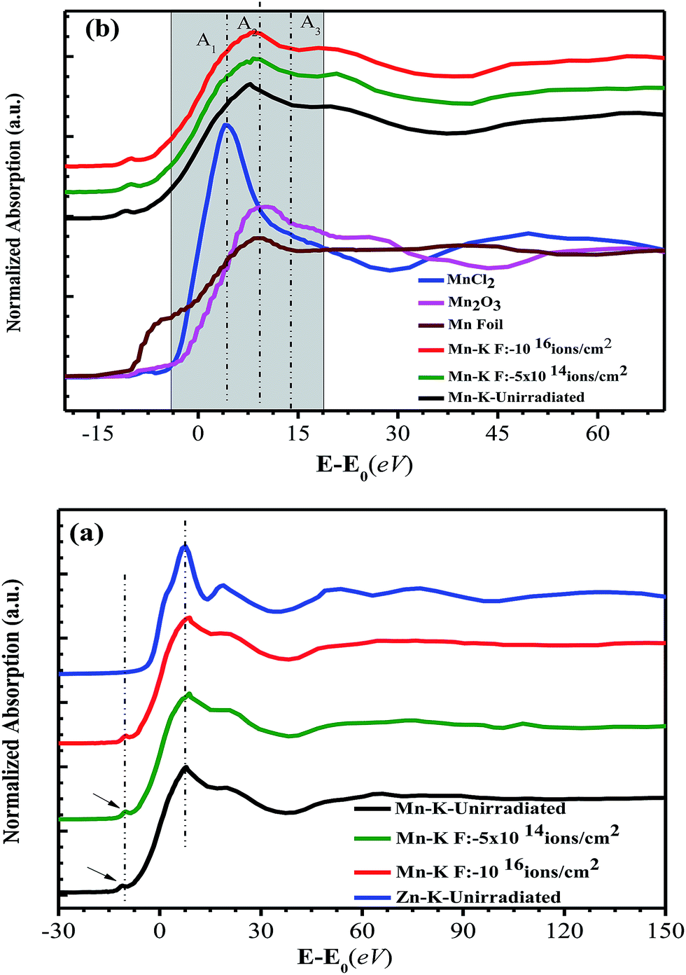
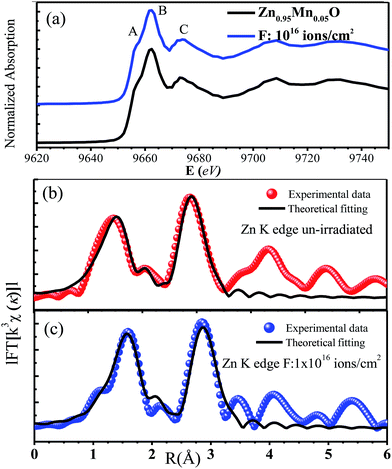
Fig. 7a exhibits XANES curves for Mn-K and Zn-K edges of un-irradiated and irradiated (fluence: 5 × 10¹⁴ and 1016 ions per cm2) Zn0.95Mn0.05O films at RT as a function of (E − Eo), where E is the incident X-ray energy and Eo is the absorption edge energy. The Eo for different films can be obtained by taking the 1st peak of the 1st derivative of μ(E) versus E curve.46 This rescaling of energy helps to compare the respective absorption K edges (Mn-K and Zn-K edges) of the films. The features of Mn K edges are as follows: a small pre edge peak (∼6539 eV), the dominant main peak, and the shoulder at the post edge region. This pre edge peak is characteristic of TM ions originated due to transition between Mn 1s core electron to the un-occupied Mn-3d and O-2p hybridized states.46,47 However, Mn-K absorption features is different from that of Zn-K edge features in the energy interval −10 eV to 80 eV as highlighted in Fig. 7a, indicating chemical environment of Mn is different from Zn in ZnO.48 Further the respective Mn-K edges of reference Mn foil, MnCl2, Mn2O3 samples are presented in Fig. 7b. The absorption features as highlighted by A1, A2, A3 indicates a mixed valance state of Mn (Mn2+ and Mn3+) in the films.26,46 So, a part of Mn ions is in 2+ state and substituted the Zn2+ ions in ZnO and the remaining Mn ions are in 3+ charge state. Further, no such significant change in the spectral shape, edge positions and also in pre edge transition (∼6539 eV) of Mn-K edges of respective films were noticed. So, any segregation of metallic Mn in the form of cluster in the host structure hasn't been taken place. In fact, during synthesis of these films, the first heat treatment was performed at 300 °C. The solvent (2-propanol) at 300 °C temperature has a very low reduction activity therefore it is difficult that Mn ions to be reduced to metallic cluster.49
 |
| | Fig. 7 (a) Normalized Mn-K edges XANES spectra un-irradiated and irradiated films. The Zn-K edge XANES spectrum of un-irradiated sample is also plotted in the same panel for comparison. (b) Normalized Mn-K edges XANES spectra of the respected films along with Mn-K edges of standard materials. | |
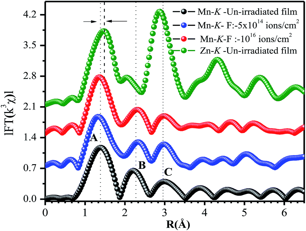
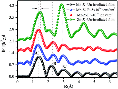
Fig. 8 depicts the FT-EXAFS spectra of Mn-K edge for un-irradiated and irradiated films and Zn-K edge spectrum of un-irradiated film was also shown. In Mn-K edge FT-EXAFS spectra, three peaks (A, B, C) can be clearly identified at about 1.39 Å, 2.3 Å and 2.9 Å suggesting local structure surrounding Mn atom is different from that of Zn atom. This fact was further supported from difference in nature of variation of EXAFS oscillation at Mn-K and Zn-K edges (Fig. 7a) and detection of mixed valance oxidation state for Mn (Fig. 7b), consistent with reported result.26 When Mn is incorporated at interstitial site, it forms Mn3+O6 octahedron and when Mn occupies substitutional site it forms Mn2+O4 tetrahedron.26,46 In the Mn-K edge FT-EXAFS spectra, the extra peak B in between A and C also indicates that a fraction of Mn atoms goes to interstitial sites of wurtzite ZnO and forms Mn3+O6 octahedra. The simultaneous presence of peaks A, B and C indicates that Mn is at substitutional position as well as at interstitial site in the ZnO lattice. Interestingly, it is observed that the first peak ∼1.49 Å corresponding to Zn–O bond length for Zn-K edge is shifted to ∼1.39 Å in case of Mn-K edge FT-EXAFS pattern and becomes broad. Actually, this particular peak contains simultaneous contribution of first Mn–O coordination shell of Mn2+O4 and Mn3+O6 configurations. The peak B is solely contributed by second Mn–Mn coordination shell of Mn3+O6 and peak C is the Mn–Zn(Mn) coordination of Mn2+O4 in Zn0.95Mn0.05O. Further, the intensity ratio of peak C and peak B has been found to be relatively higher for irradiated film of low fluence 5 × 10¹⁴ ions per cm2 than that of Zn0.95Mn0.05O and high fluence (1016 ions per cm2) irradiated film. This fact also indicates that the relative content of Mn at substitutional positions is higher for the film irradiated with fluence 5 × 10¹⁴ ions per cm2. Moreover, concentrations of VO are also comparatively less due to release of O atoms from MnO6 with transformation of MnO6 to MnO4 in this particular irradiated (fluence 5 × 10¹⁴ ions per cm2) film. This fact is also supported from PL study with the observation of increasing number of VZns and simultaneous decrease in concentrations of VO together reduce the overall luminescence in the visible region for this irradiated film (fluence 5 × 10¹⁴) with respect to other films. It was found from the local structure study that Mn ions in ZnO lattice with octahedral coordination of Mn gives rise to AFM interaction that inhibits FM. Hence, the film with low irradiation fluence exhibits strongest FM in absence of AFM coupling, possibly connected with the fact that more Mn spins are tetrahedrally coordinated (i.e., better substitutional incorporation of Mn at the position of Zn).26,45
 |
| | Fig. 8 FT EXAFS spectra of Zn-K edge of un-irradiated and Mn-K edges of un-irradiated, irradiated films with fluence 5 × 10¹⁴ and 1016 ions per cm2 respectively. | |
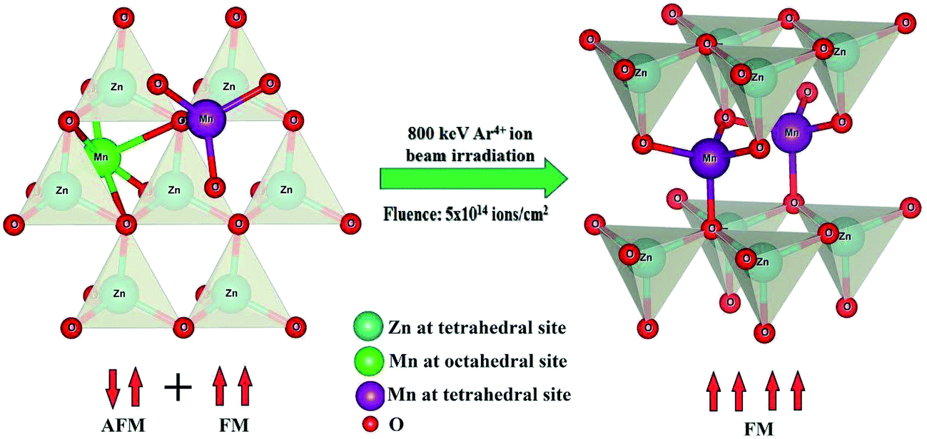
Increase in tetrahedral coordination of Mn and decrease in concentration of VO have been steamed out from local structure analysis and PL study, indeed an interesting observation of highly correlated magnetic, optical and micro-structural properties for a system of un-irradiated and Ar4+ ion irradiated Zn0.95Mn0.05O films. It is an important point to note that low energy (800 keV) Ar4+ ion irradiation with a particular fluence 5 × 10¹⁴ ions per cm2 can develop AFM coupling free strong FM in Mn doped ZnO film. Possibly at low fluence 5 × 10¹⁴ ions per cm2, a major number of Mn ions transforms into tetrahedral coordination from octahedral coordination and subsequently suppresses the formation of VO. In this context, one point to be noted that intrinsic FM of Mn doped ZnO dependent on both factors, viz. overlapping BMP formation18 and substitutional occupation of Mn ions at Zn site.20 Further, the displacement of Mn ions from interstitial to substitutional position by ion irradiation due to impact of energetic ions is rather a dynamic and highly complex process otherwise it will only be dependent on energy not on fluence. Hence, ion irradiation of energy 800 keV and fluence 5 × 10¹⁴ ions per cm2 can be considered as the optimized parameters at least from this study for generating AFM coupling free strong FM in Mn doped ZnO film. The suppression in strength of AFM coupling between Mn ions at low fluence (5 × 10¹⁴ ions per cm2) and its probable association with decreasing proportion of interstitial (octahedral) Mn ions have been schematically represented in Fig. 9. Fluence dependent low energy ion beam irradiation may induce a kind of micro-structural transition (displacement of Mn ions from interstitial to substitutional position), which is manifested as highly desired macro (bulk) magnetic property (strong FM) in DMS ZnO and EXAFS study actually unfolds this micro-structural transition.
 |
| | Fig. 9 Schematic diagram of proposed transformation of AFM coupling free ferromagnetic sample associated with decreasing interstitial Mn contribution from un-irradiated film to Ar4+ ion irradiated film (fluence: 5 × 10¹⁴ ions per cm2). | |
Conclusion
The study on structural, optical, magnetic and micro-structural properties of low energy (800 keV) Ar4+ ion irradiated and un-irradiated Zn0.95Mn0.05O films unveiled interesting observations. All single-phase films exhibit RT FM and nice variation with fluence of irradiation. Actually the low fluence: 5 × 10¹⁴ ions per cm2 of irradiation is causing transformation of more number of Mn ions from interstitial (octahedral coordination) to substitutional (tetrahedral coordination) position thereby suppressing VO and develops AFM coupling free strong FM. The low fluence of ion irradiation has been supposed to be optimized for synthesizing the strong magnetic film. Further, a correlated magnetic, micro-structural and optical property of Zn0.95Mn0.05O films has been generated upon low energy ion irradiation. The high transparency of the films enhances potential for transparent electrode besides spin electronic application.
Acknowledgements
First and second author contribute equally in this work. Md. A. A acknowledges UGC for providing his Research fellowship. Authors thank the Department of Science and Technology, India for the financial support and Saha Institute of Nuclear Physics, India for facilitating the powder XRD experiments at the Indian Beamline (BL-18B), Photon Factory, KEK, Japan. We acknowledge IUAC, India for irradiation(LEIBF) and RBS experiments and RRCAT, India for the XANES and EXAFS measurements utilizing their dispersive EXAFS beam line (BL 8) of INDUS 2 Synchrotron Source (2.0 GeV, 100 mA). We acknowledge UGC DAE CSR, KC and IUAC, New Delhi, India for financial support through CRS and UFUP scheme [UFR-55301] respectively.
References
- N. H. Hong, J. Sakai and A. Hassini, Appl. Phys. Lett., 2004, 84, 2602 CrossRef CAS.
- J. M. D. Coey, A. P. C. Douvalis, B. Fitzgerald and M. Venkatesan, Appl. Phys. Lett., 2004, 84, 1332 CrossRef CAS.
- T. Dietl, H. Ohno, F. Matsukura, J. Cibert and D. Ferrand, Science, 2000, 287, 1019 CrossRef CAS PubMed.
- L. H. Ye, A. J. Freeman and B. Delley, Phys. Rev. B: Condens. Matter Mater. Phys., 2006, 73, 033203 CrossRef.
- K. Sato, L. Bergqvist, J. Kudrnovský, P. H. Dederichs, O. Eriksson, I. Turek, B. Sanyal, G. Bouzerar, H. K. Yoshida, V. A. Dinh, T. Fukushima, H. Kizaki and R. Zeller, Rev. Mod. Phys., 2010, 82, 1633 CrossRef CAS.
- P. Sharma, A. Gupta, K. V. Rao, F. J. Owens, R. Sharma, R. Ahuja, J. M. O. Guillen, B. Johansson and G. A. Gehring, Nat. Mater., 2003, 2, 673 CrossRef CAS PubMed.
- S. Chattopadhyay, S. K. Neogi, A. Sarkar, M. D. Mukadam, S. M. Yusuf, A. Banerjee and S. Bandyopadhyay, J. Magn. Magn. Mater., 2011, 323, 363 CrossRef CAS.
- S. Chattopadhyay, S. Dutta, A. Banerjee, D. Jana, S. Bandyopadhyay, S. Chattopadhyay and A. Sarkar, Phys. B, 2009, 404, 1509 CrossRef CAS.
- S. K. Neogi, R. Ghosh, G. K. Paul, S. K. Bera and S. Bandyopadhyay, J. Alloys Compd., 2009, 487, 269 CrossRef CAS.
- R. Karmaker, S. K. Neogi, A. Banerjee and S. Bandyopadhyay, Appl. Surf. Sci., 2012, 263, 671 CrossRef.
- M. Ivill, S. J. Pearton, Y. W. Heo, J. Kelly, A. F. Hebard and D. P. Norton, J. Appl. Phys., 2007, 101, 123909 CrossRef.
- W. Liu, W. Li, Z. Hu, Z. Tang and X. Tang, J. Appl. Phys., 2011, 110, 01390 CrossRef PubMed.
- K. Yuan, Q. X. Yu, Q. Q. Gao, J. Wang and X. T. Zhang, Appl. Surf. Sci., 2012, 258, 3350 CrossRef CAS.
- W. Yan, Z. Sun, Q. Liu, Z. Li, Z. Pan, J. Wang and S. Wei, Appl. Phys. Lett., 2007, 91, 062113 CrossRef.
- W. Yan, Z. Sun, Q. Liu, Z. Li, T. Shi, F. Wang, Z. Qi, G. Zhang, S. Wei, H. Zhang and Z. Chen, Appl. Phys. Lett., 2007, 90, 242509 CrossRef.
- J. M. D. Coey, M. Venkatesan and C. B. Fitzgerald, Nat. Mater., 2005, 4, 173 CrossRef CAS PubMed.
- K. R. Kittilstved and D. R. J. Gamelin, Am. Chem. Soc., 2005, 127, 5292 CrossRef CAS PubMed.
- S. K. Neogi, N. Midya, P. Pramanik, A. Banerjee, A. Bhattacharya, G. S. Taki, J. B. M. Krishna and S. Bandyopadhyay, J. Magn. Magn. Mater., 2016, 408, 217 CrossRef CAS.
- S. K. Neogi, S. Chattopadhyay, A. Banerjee, S. Bandyopadhyay, A. Sarkar and R. Kumar, J. Phys.: Condens. Matter, 2011, 23, 205801 CrossRef CAS PubMed.
- S. K. Neogi, S. Chattapadhyay, R. Karmakar, A. Banerjee, S. Bandyopadhyay and A. Banerjee, J. Alloys Compd., 2013, 573, 76 CrossRef CAS.
- R. P. Borges, R. C. Silva, S. Magalhaes, M. M. Cruz and M. Godinho, J. Phys.: Condens. Matter, 2007, 19, 476207 CrossRef.
- S. K. Neogi, R. Karmakar, A. K. Misra, A. Banerjee, D. Das and S. Bandyopadhyay, J. Magn. Magn. Mater., 2013, 346, 130 CrossRef CAS.
- A. K. Yadav, S. M. Haque, S. Tripathi, D. Shukla, M. A. Ahmed, D. M. Phase, S. Bandyopadhyay, S. N. Jha and D. Bhattacharyya, RSC Adv., 2016, 6, 74982 RSC.
- N. Smolentsev, A. V. Soldatov, G. Smolentsev and S. Q. Wei, Solid State Commun., 2009, 149, 1803 CrossRef CAS.
- L. Zhang, J. Li, Y. Du, J. Wang, X. Wei, J. Zhou, J. Cheng, W. Chu, Z. Jiang, Y. Huang, C. Yan, S. Zhang and Z. Wu, New J. Phys., 2012, 14, 013033 CrossRef.
- C. Yan, H. W. Chang, L. W. Xian, X. H. Zhe, C. Rui and D. S. Xue, Chin. Phys. B, 2013, 22, 107501 CrossRef.
- S. Basu, D. Y. Inamdar, S. Mahamuni, A. Chakrabarti, C. Kamal, G. R. Kumar, S. N. Jha and D. Bhattacharyya, J. Phys. Chem. C, 2014, 118, 9154 CAS.
- B. Kharroubi, R. Baghdad, A. Abdiche, M. Bousmaha, M. Bousquet, A. Zeinert, M. E. Marssi, K. Zellama and S. Hamzaoui, Phys. Scr., 2012, 86, 015805 CrossRef.
- Y. Caglar, J. Alloys Compd., 2013, 560, 181 CrossRef CAS.
- S. Chattopadhyay, S. Dutta, D. Jana, S. Chattopadhyay, A. Sarkar, P. Kumar, D. Kanjilal, D. K. Mishra and S. K. Ray, J. Appl. Phys., 2010, 107, 113516 CrossRef.
- P. K. Giri, S. Bhattacharyya, D. K. Singh, R. Kesavamoorthy, B. K. Panigrahi and K. G. M. Nair, J. Appl. Phys., 2007, 102, 093515 CrossRef.
- S. Bandyopadhyay, G. K. Paul and S. K. Sen, Sol. Energy Mater. Sol. Cells, 2002, 71, 103 CrossRef CAS.
- S. Dutta, S. Chattopadhyay, A. Sarkar, M. Chakrabarti, D. Sanyal and D. Jana, Prog. Mater. Sci., 2009, 54, 89 CrossRef CAS.
- S. K. Mishra, R. K. Srivastava, S. G. Prakash, R. S. Yadav and A. C. Panday, Opto-Electron. Rev., 2010, 18(4), 467 CAS.
- W. Liu, W. Li, Z. Hu, Z. Tang and X. Tang, J. Appl. Phys., 2011, 110, 013901 CrossRef.
- M. Diaconu, H. Schmidt, H. Hochmuth, M. Lorenz, G. Benndorf, J. Lenzner, D. Spemann, A. Setzer, K. W. Nielsen, P. Esquinazi and M. Grundmann, Thin Solid Films, 2005, 486, 117 CrossRef CAS.
- S. Yang and Y. Zhang, J. Magn. Magn. Mater., 2013, 334, 52 CrossRef CAS.
- S. P. Pati, A. K. Mishra, S. Kumar and D. Das, J. Phys. Chem. Solids, 2013, 74, 811 CrossRef.
- G. Li, C. W. Leung, C. Shueh, Y. J. Wu, K. W. Lin, A. C. Sun, J. H. Hsu, P. T. Lai and P. W. T. Pong, Surf. Coat. Technol., 2013, 228, 354 CrossRef.
- G. Li, C. W. Leung, Y. J. Wu, A. C. Sun, J. H. Hsu, P. T. Lai, K. W. Lin and P. W. T. Pong, Microelectron. Eng., 2013, 110, 250 CrossRef CAS.
- G. Li, C. W. Leung, C. Shueh, H. F. Hsu, H. R. Huang, K. W. Lin, P. T. Lai and P. W. T. Pong, Surf. Coat. Technol., 2013, 228, 437 CrossRef.
- Y. M. Kim, M. Yoon, I. W. Park, Y. J. Park and J. H. Lyou, Solid State Commun., 2004, 129, 175 CrossRef CAS.
- H. B. Ruan, L. Fang, G. P. Qin, T. Y. Yang, W. J. Li, F. Wu, M. Saleem and C. Y. Kong, Solid State Commun., 2012, 152, 1625 CrossRef CAS.
- J. Haug, A. Chassé, M. Dubiel, C. Eisenschmidt, M. Khalid and P. Esquinazi, J. Appl. Phys., 2011, 110, 063507 CrossRef.
- Y. Cheng, W. Hao, H. Xu, Y. X. Yu, T. Wang, R. Chen, L. Zhang, Y. Du, X. L. Wang and S. X. Dou, ACS Appl. Mater. Interfaces, 2012, 4, 4470 CAS.
- Y. Cheng, R. Chen, H. Feng, W. Hao, H. Xu, Y. Wang and J. Li, Phys. Chem. Chem. Phys., 2014, 16, 4544 RSC.
- H. S. Hsu, J. C. A. Huang, Y. H. Huang, Y. F. Liao, M. Z. Lin, C. H. Lee, J. F. Lee, S. F. Chen, L. Y. Lai and C. P. Liu, Appl. Phys. Lett., 2006, 88, 242507 CrossRef.
- N. R. S. Farley, K. W. Edmonds, A. A. Freeman, G. V. D. Laan, C. R. Staddon, D. H. Gregory and B. L. Gallagher, New J. Phys., 2008, 10, 055012 CrossRef.
- T. Yao, W. Yan, Z. Sun, Z. Pan, B. He, Y. Jiang, H. Wei, M. Nomura, Y. Xie, T. Hu and S. Wei, J. Phys. Chem. C, 2009, 113, 3581 CAS.
Footnote |
| † Electronic supplementary information (ESI) available: SRIM simulation results of the energy loss of Ar ions and penetration depth of Ar ions inside the samples along with defect creation of ion beam inside the target due to impact of ion beam has been mentioned. See DOI: 10.1039/c6ra25233h |
|
| This journal is © The Royal Society of Chemistry 2017 |
Click here to see how this site uses Cookies. View our privacy policy here. 
 Open Access Article
 This Open Access Article is licensed under a