
 Open Access Article
 This Open Access Article is licensed under a
 Creative Commons Attribution 3.0 Unported Licence
Enhancement of photocurrent in an ultra-thin perovskite solar cell by Ag nanoparticles deposited at low temperature†
Yang Liu*ab,
Felix Langa,
Thomas Dittricha,
Alexander Steigerta,
Christian-Herbert Fischerb,
Tristan Köhlera,
Paul Platea,
Jörg Rappicha,
Martha Ch. Lux-Steinera and
Martina Schmid*ac
aHelmholtz-Zentrum Berlin für Materialien und Energie GmbH, Hahn-Meitner-Platz 1, 14109 Berlin, Germany. E-mail: yang.liu@helmholtz-berlin.de; martina.schmid@helmholtz-berlin.de
bFreie Universität Berlin, Institute of Chemistry and Biochemistry, Fabeckstr. 34-36, 14195 Berlin, Germany
cFreie Universität Berlin, Department of Physics, Arnimallee 14, 14195 Berlin, Germany
First published on 4th January 2017
Abstract
Ultra-thin perovskite absorber layers have attracted increasing interest since they are suitable for application in semi-transparent perovskite and tandem solar cells. In this study, size and density controlled plasmonic silver nanoparticles are successfully incorporated into ultra-thin perovskite solar cells through a low temperature spray chemical vapor deposition method. Incorporation of Ag nanoparticles leads to a significant enhancement of 22.2% for the average short-circuit current density. This resulted in a relative improvement of 22.5% for the average power conversion efficiency. Characterization by surface photovoltage and photoluminescence provides evidence that the implemented silver nanoparticles can enhance the charge separation and the trapping of electrons into the TiO2 layer at the CH3NH3PbI3/TiO2 interface. The application of these silver nanoparticles therefore has promise to enhance the ultra-thin perovskite solar cells.
Introduction
In recent years, the inorganic–organic hybrid perovskites have attracted extremely high attention.1 They have many advantages, e.g., they can be processed by very simple, low cost methods and in parallel they have excellent electrical and optical properties.2 The perovskite solar cell (PSC) power conversion efficiency (PCE) has sharply improved from the 3.81% first reported in 2009 to 22.1% in 2016.3,4 Early-stage PSCs had a similar architecture as dye-sensitized solar cells, employing a mesoporous metal oxide (normally TiO2) layer for electron transfer.5,6 Later, Snaith et al. found electrons can be transported through the perovskite absorber layer.7 This opened the gate for developing the planar heterojunction PSCs which further expanded the scope of application of PSCs.8–10 Based on the development of planar heterojunction PSCs, ultra-thin perovskite absorber layers which are much thinner than the perovskite absorber layers in normal PSCs became widely used and find application in semitransparent PSCs and tandem solar cells.11–14 However, due to the decrease of the layer thickness, the ultra-thin perovskite solar cells (UTPSCs) cannot give PCEs comparable to the bulk PSCs.9,11To improve the PCE of solar cells without increasing the thickness of the absorber layer, the implementation of plasmonic nanoparticles has proved beneficial.15,16 Plasmonic nanoparticles can increase the effective light absorption of the absorber layer through plasmonic effects.15–17 This has been confirmed by the application of plasmonic nanoparticles in different kinds of solar cells, for example, in silicon solar cell,18 in organic solar cell19 or in ultra-thin chalcopyrite solar cell.20 Hence, it is a promising way to use the same method to improve the PCE of perovskite solar cells. Although very interesting work has been reported on plasmonic enhanced PSCs, most of the nanoparticles were pre-synthesized and then implemented into the PSCs.21–26 That can be a drawback for the application in large scale PSCs. Moreover, several groups used Au nanoparticles for the plasmonic enhancement, which can dramatically increase the cost.24,26
In this work, a spray chemical vapor deposition method (spray-CVD)27,28 was used for one step implementation of size and density controlled silver nanoparticles (Ag NPs) into UTPSC. The spray-CVD used here can easily be applied on large scale and the temperature used is much lower than that of the similar method reported in other work.29–32 The thickness of the perovskite absorber layer used is around 140 nm, which is much thinner than the normal thickness (∼300 nm or even thicker). By implementation of Ag NPs, a significant enhancement of the short-circuit current density (Jsc) by 22.2% was obtained for the averaged performance of the solar cells, leading to a relative improvement of efficiency by 22.5%. As confirmed by surface photovoltage (SPV) and photoluminescence (PL) study, the implemented Ag NPs can enhance charge separation and electron transfer to TiO2 layer, hence increase the photocurrent.
Experimental details
Materials
Commercial fluorine-doped tin oxide (FTO) glasses (∼8 Ω sq−1) were received from Solaronix. Acetone, ethanol, titanium diisopropoxide bis(acetylacetonate) (Ti(acac)2OiPr2), lead iodide (PbI2), γ-butyrolactone (GBL) and dimethyl sulfoxide (DMSO), toluene, 4-tert-butylpyridine (tBP), bis(trifluoromethane) sulfonimide lithium salt (LiTFSI), acetonitrile (ACN), chlorobenzene (CBZ) were purchased from Sigma-Aldrich. Trimethylphosphine (hexafluoroacetylacetonato) silver (Ag(hfacac)PMe3) were purchased from Strem Chemicals Inc. Methylammonium iodide (MAI) was received from DyeSol. 2,2′,7,7′-Tetrakis(N,N-di-4-methoxy-phenyl-amino)-9,9′-spirobifluorene (spiro-OMeTAD) was purchased from 1-Material Inc. The purity of gold (Au) used for electrodes was 99.999%. All the chemicals were used as received.Silver nanoparticles deposition
Ag NPs were deposited on clean FTO/glass substrates by spray chemical vapor deposition. The precursor solution was prepared by dissolving Ag(hfacac)(PMe3) in ethanol with a concentration of 10 mM. The precursor solution was nebulized to form an aerosol which was carried by nitrogen gas to the FTO glass substrate. The nitrogen flow rate was controlled to be 1 liter per minute and the substrate temperature was set to 110 °C during the deposition process. The deposition time was adjusted to 0.5, 1 and 5 min in order to vary the size (diameter from SEM) of the Ag NPs. The FTO glass substrates without Ag NP deposition were used as control samples.Ultra-thin perovskite solar cell fabrication
FTO glass substrates (2.35 cm × 2.35 cm) were cleaned by sonication in de-ionized water, acetone and ethanol for 20 min in each solvent and blown dry with nitrogen afterwards. The substrates were further cleaned by an Ar plasma treatment for 5 min. The compact TiO2 layer was deposited onto the cleaned FTO glass substrates with or without Ag NPs by spray pyrolysis using titanium diisopropoxide bis(acetylacetonate) as precursor. The concentration of the precursor solution and the substrate temperature were 6.8 mM and 460 °C, respectively. After the deposition of the compact TiO2 layer, all samples were transferred into a glove box with a H2O and O2 level less than 0.1 ppm. A stoichiometric CH3NH3PbI3 precursor solution with a concentration of 0.8 M was prepared by dissolving PbI2 and MAI in 1 mL mixed solvent from 0.7 mL GBL and 0.3 mL DMSO. The solution was then stirred at 60 °C for 12 h. An ∼140 nm thick CH3NH3PbI3 layer was deposited by spin coating the CH3NH3PbI3 solution at 1000 rpm for 10 s and 5000 rpm for 20 s. For each speed, there were 5 s for increasing from 0 or 1000 rpm to the desired speed. At 35 s of the spin coating step, 150 μL of toluene was dripped onto the samples. The obtained CH3NH3PbI3 layer was annealed on a hot plate at 100 °C for 10 min. Details of the corresponding process can be found elsewhere.33 After the sample had cooled down to room temperature, a layer of spiro-OMeTAD was deposited onto the perovskite layer by spin coating at 2000 rpm for 40 s. The precursor solution of spiro-OMeTAD was prepared by dissolving 72.3 mg spiro-OMeTAD in 1 mL CBZ, and then adding 17.5 μL tBP and 46.4 μL LiTFSI solution (170 mg mL−1 in ACN). Finally, gold back contacts with a thickness of 80 nm were deposited by thermal evaporation to finish the fabrication of the solar cells.Characterization
The morphology of the Ag NPs and the thicknesses of each layer in the perovskite solar cell were studied by a scanning electron microscope (SEM, Gemini LEO1530 system) with an in-lens detector. The crystal structures of Ag NPs and the TiO2 layer were studied by X-ray diffraction (XRD) with a Bruker D8 X-ray diffractometer operated in the gracing incidence mode with irradiation by a Cu Kα source. Transmission and reflection spectra were measured using a Lambda 950 spectrophotometer with an integrating sphere. Absorption spectra were obtained by subtracting transmission and reflection from 100%. The surface of the samples before deposition of the perovskite layer was measured by X-ray photoelectron spectroscopy (XPS). Mg Kα (1253.6 eV) radiation from a SPECS XR 50 X-ray gun served as excitation source. The emitted photoelectrons were detected by a CLAM 4 electron spectrometer from Thermo VG Scientific. Charge separation and transport length (L) of photo-generated charge carriers were studied by SPV measurements.34–37 In the measurement of L, the SPV signal is kept constant whereas the light intensity is plotted depending on the absorption length (Goodman plot). The intersection point of the corresponding linear fit gives the negative value of L.36,37 PL was measured using lasers of two wavelengths, 362 nm and 504 nm. For both SPV and PL measurements, the light incident through the glass side. The samples didn't have a spiro-OMeTAD layer and Au back contact, instead a PMMA layer was deposited on top of the perovskite layer for the samples used in SPV measurements.34 Current–voltage (J–V) curves of perovskite solar cells were measured using a “Steuernagel Lichttechnik” sun simulator, imitating an AM 1.5G spectra. The effective area of the solar cell was defined as 0.16 cm2 by the Au electrode. All J–V curves were measured in both forward (from negative to positive) and reverse direction. The delay time and acquisition time were set as 40 ms and 20 ms, respectively, leading to a scan speed of 0.167 V s−1. External quantum efficiency (EQE) spectra were measured by a specially designed EQE system in the wavelength range of 300–850 nm.Results and discussion
Performance and architecture of ultra-thin perovskite solar cells with and without Ag NPs
Fig. 1a shows the cross sectional SEM image of UTPSC without integration of Ag nanoparticles. A dense ∼35 nm thin TiO2 layer was first deposited on top of the FTO/glass substrate by spray pyrolysis, and then a continuous and uniform ultra-thin CH3NH3PbI3 perovskite layer (∼140 nm) was deposited. Afterwards a hole conducting spiro-OMeTAD layer was spin coated on top, an Au back contact layer was evaporated last to finish the fabrication of the perovskite solar cell. Fig. 1b illustrates the schematic structure of the UTPSC. It has to be mentioned that the efficiency limit of the UTPSCs with 140 nm thick perovskite layer is approximately 24% which is lower than that of 31% for standard PSCs.38 To the best of the authors' knowledge, reported efficiencies of the UTPSCs with around 140 nm thick perovskite layer are lower than 15%.11–13,39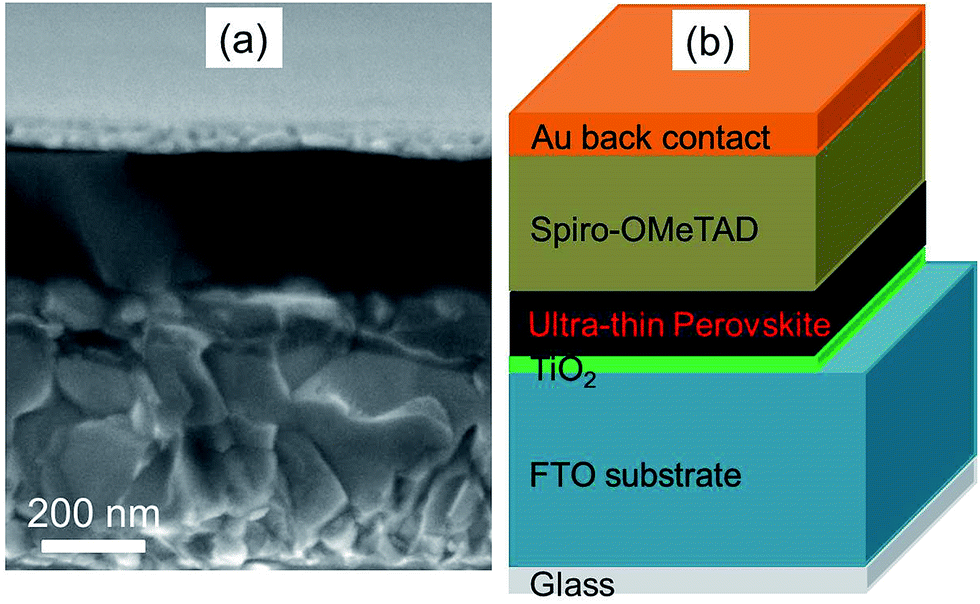 | ||
| Fig. 1 (a) Cross sectional SEM image of ultra-thin perovskite solar cell. (b) Schematic device structure of ultra-thin perovskite solar cell. | ||
By J–V measurements, the effect of Ag NPs on the performance of UTPSCs was investigated. Fig. 2a shows the schematic structure of UTPSC with integration of Ag NPs at the TiO2/FTO interface. In all the figures, a schematic structure of the samples used for each measurement is shown to facilitate understanding. Fig. 2b presents J–V curves of the best UTPSCs with and without Ag NPs selected from more than 20 devices. Diameters of Ag NPs varied from 11 nm to 16 nm. In the content afterwards, the UTPSC without Ag NPs is named as control sample while the UTPSCs with 11 nm and 16 nm Ag NPs are named as 11 nm Ag NP sample and 16 nm Ag NP sample, respectively. The control sample exhibited 1.02 V open circuit voltage (Voc), Jsc = 14.07 mA cm−2, and Fill Factor (FF) = 0.58, leading to a PCE of 8.28%. With implementation of different sizes of Ag NPs, Voc of the UTPSCs decreases from 1.02 V to 0.99 V (both 11 nm and 16 nm Ag NP sample). This can be due to the Ag NPs acting as recombination center in the UTPSCs.26,34 However, Jsc of the UTPSCs first increases from 14.04 mA cm−2 of the control sample to 15.93 mA cm−2 of the 11 nm Ag NP sample (13.5% increase compared to the control sample), then increases less to 15.83 mA cm−2 for the 16 nm Ag NP sample (12.7% increase compared to control sample). FF of the 11 nm Ag NP sample is 0.58 which is the same as the control sample while for the 16 nm Ag NP sample FF is 0.54 which is a bit lower. The increase of Jsc leads to the increase of PCE from 8.28% for the control sample to 9.14% for the 11 nm Ag NP sample and 8.40% for the 16 nm Ag NP sample. The relative increase of PCE by incorporating 11 nm and 16 nm Ag NPs are 10.4% and 1.4%, respectively. Due to the decrease of Voc, the increase of PCE is not as high as the one in Jsc.
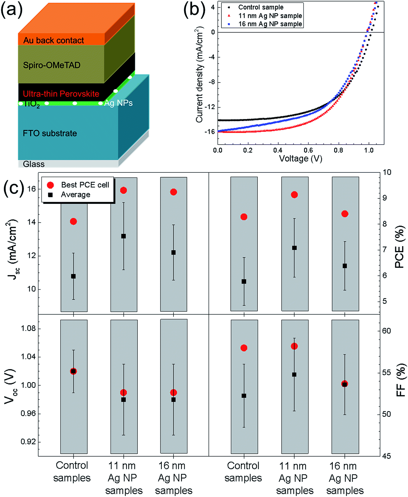 | ||
| Fig. 2 (a) Schematic device structure of ultra-thin perovskite solar cell with incorporation of Ag nanoparticles at the TiO2/FTO interface. (b) J–V curves of the best PCE ultra-thin perovskite solar cells without, with 11 nm and with 16 nm Ag NPs (i.e. control sample, 11 nm Ag NP sample and 16 nm Ag NP sample). (c) Average device performances of control samples, 11 nm Ag NP samples and 16 nm Ag NP samples measured by reverse scan. For each condition, more than 20 devices were fabricated and measured. | ||
To ensure the reliability of the enhancement, more than 20 devices were prepared for each configuration in three batches. The average device performance parameters are presented in Fig. 2c. For the 11 nm Ag NP samples, an average Jsc of 13.19 mA cm−2 was achieved, which is 22.2% higher than the average Jsc of 10.79 mA cm−2 for the control samples. At the same time, the average Jsc is 12.21 mA cm−2 for the 16 nm Ag NP samples, which is 13.2% higher than that of the control samples. The average FF of 11 nm Ag NP samples is 0.55 while that of 16 nm Ag NP samples is 0.54, both of which are higher than 0.52 for the control samples. The increase of both Jsc and FF leads to the improvements of the average PCE from 5.78% for the control samples to 7.08% (22.5% relative) for the 11 nm Ag NP samples and to 6.38% (10.5% relative) for the 16 nm Ag NP samples. Therefore, it's confirmed that the incorporation of Ag NPs can improve the device performance of UTPSC by enhancing the photocurrent. It has to be pointed out that in each batch the enhancement of Jsc and PCE by incorporating Ag NPs has the same trend (shown in Fig. S1†). The consistency of the enhancement in different batches confirmed again the influence of Ag NPs on UTPSCs. However, it is also observed that Voc decreased clearly due to the integration of both 11 nm and 16 nm Ag NPs, which lowers the increase of average PCE for both the 11 nm and 16 nm Ag NPs samples. If the decrease of Voc can be prevented, higher improvement of PCE can be expected.
Fig. 2 shows the reverse scan performances of the UTPSCs. Fig. S2† presents the hysteresis performances of the best control, 11 nm Ag NP and 16 nm Ag NP samples. Fig. S3† shows the average forward scan performances of the same samples shown in Fig. 2c, the differences agreed well with the reverse scan behavior. In addition, Fig. S4† shows the Voc and Jsc histogram of the control samples and of the 11 nm Ag NP samples. Gaussian fitting for these four histograms confirmed the increase of Jsc and decrease of Voc caused by the incorporation of 11 nm Ag NPs in the UTPSCs.
To understand the mechanism of the photocurrent enhancement and decrease of Voc caused by the integration of Ag NPs, different kinds of characterization were carried out.
Morphology, optical properties of Ag nanoparticles and stabilization by TiO2 layer
SEM images of FTO substrates without and with different sizes of Ag NPs are presented in Fig. 3b–e. Fig. 3a shows the structure of Ag NPs on top of FTO coated glass substrate. Sizes of the Ag NPs are 11 nm (Fig. 3c), 16 nm (Fig. 3d) and 36 nm (Fig. 3e), and they were prepared by simple variation of the deposition time using low temperature (110 °C) spray CVD. It is observed that in all three cases the sizes of the Ag NPs varied little, which can be recognized as nearly mono-dispersed. It has to be pointed out that the temperature of 110 °C used to deposit Ag NPs was much lower than the reported work using spray pyrolysis to form Ag NPs.29–32 This low temperature, size and density controlled Ag NPs deposition method has high potential for wide use in different applications.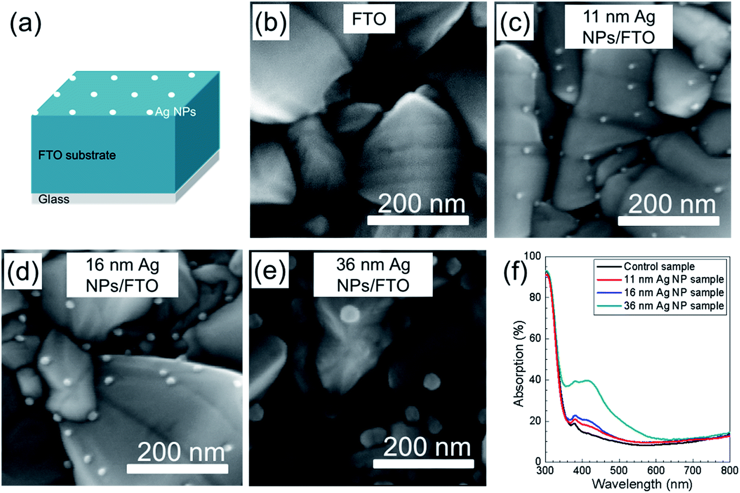 | ||
| Fig. 3 (a) Schematic sample structure of Ag NPs on top of FTO coated glass substrate. (b–e) SEM images of FTO coated glass substrates without (b) and with 11 nm Ag NPs (c), 16 nm Ag NPs (d), 36 nm Ag NPs (e) on top. (f) UV-Vis absorption spectra of FTO coated glass substrate and with different sizes of Ag NPs on top. | ||
Optical properties of Ag NPs deposited on FTO substrates were studied by UV-Vis measurements. Reflection and transmission of the three samples were recorded and the absorption of each sample was calculated (shown in Fig. 3f). Compared to the FTO/glass substrate, the absorption is clearly enhanced for the three Ag NP samples. The significant absorption enhancement from the 11 nm Ag NP sample to the 36 nm Ag NP sample is due to the increase of both size and coverage. In all three cases with Ag NPs (11 nm, 16 nm and 36 nm) an absorption peak around 430 nm is observed.
Fig. 4a presents the structure in which the Ag NPs on top of FTO coated glass substrate were covered by a TiO2 compact layer. Fig. 4b–e show the SEM images for the samples from Fig. 3b–e with covering of an additional TiO2 thin layer. For all the samples in Fig. 4b–e, the thin TiO2 layers were very homogeneous and followed the structure of FTO surface. Almost no Ag NPs can be observed from Fig. 4c–e, which means that all Ag NPs were covered by the TiO2 layer. In Fig. 4e, the distances between the Ag NPs nearly don't change compared to the same sample without TiO2 coating (Fig. 3e). This indicates that the Ag NPs on the surface of FTO were stabilized at their original positions by the TiO2 compact layer.
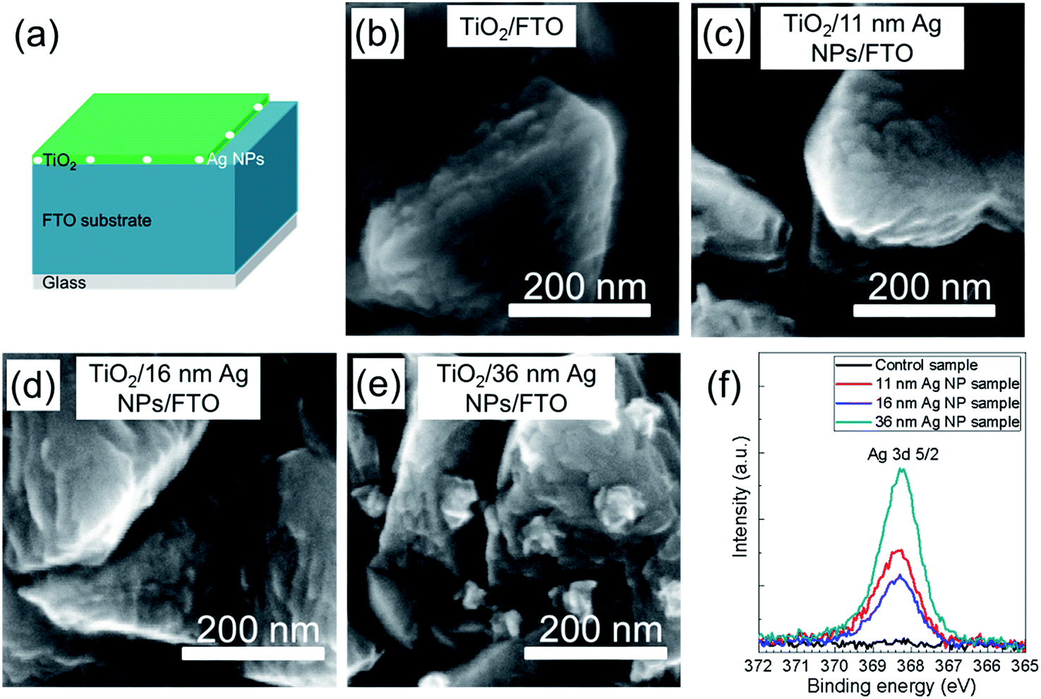 | ||
| Fig. 4 (a) Schematic sample structure of TiO2/Ag NPs/FTO/glass. (b–e) SEM images of TiO2 layer coated on FTO coated glass substrates without (b) and with 11 nm Ag NPs (c), 16 nm Ag NPs (d), 36 nm Ag NPs (e) on top. (f) XPS spectra of Ag 3d 5/2 core level measured on compact TiO2 layers, which cover the bare FTO substrate (control sample) and FTO substrates with 11 nm Ag NPs, 16 nm Ag NPs and 36 nm Ag NPs, respectively. | ||
Absorption spectra of the samples in Fig. 4b–e are shown in Fig. S5 (ESI†). Compared to the absorption spectra of the same samples before the deposition of TiO2 layers (shown in Fig. 3f) there are significant red shifts of the Ag NPs' resonance peaks. The red shifts of resonance peaks from around 430 nm to 540 nm can be attributed to the increase of refractive index of medium surrounding the Ag NPs which is caused by the deposition of TiO2 layer. As the CH3NH3PbI3 perovskite layer can convert light with wavelengths between 300 nm and ∼800 nm to electron–hole pairs, plasmonic effects of the Ag NPs with a resonance peak in that wavelength range could be exploited to enhance the performance of such perovskite solar cell.
A typical series of XPS spectra is shown in Fig. 4f. The most interesting peak is the Ag 3d 5/2 core level with a binding energy of 368.3 eV which is typically assigned to the pure Ag element. For the samples shown in Fig. 4b–e, as the TiO2 layers were very thin (∼35 nm), XPS measurements were taken to investigate whether the Ag NPs were fully covered by TiO2 layer. It is observed that there is no Ag signal detected on the control sample, but Ag signals are detected on the surface of TiO2 for all the samples with Ag NPs. With increase of particle size from 11 nm to 36 nm Ag NPs, the detected Ag signal intensity increases. Interestingly, the Ag signal intensity of the 16 nm Ag NP sample is smaller than that of 11 nm Ag NP sample. According to the XPS results, the Ag NPs are not fully covered by TiO2 or there is diffusion of Ag to the surface of TiO2. Both of the possibilities can cause the direct contact between perovskite layer and Ag NPs, leading to the formation of recombination centers at the interface between perovskite and TiO2 layer.
Although from Fig. 4c–e it looks like the shape of the Ag NPs doesn't change, it is hard to confirm from SEM images only whether the particles underneath TiO2 are still Ag NPs and whether there is significant Ag doped TiO2. To investigate this, XRD measurements were carried out. Fig. S6† gives XRD spectra for Ag NPs/glass, TiO2/glass and TiO2 covered Ag NPs/glass. Characteristic peaks of Ag (JCPDS Files no.: 04-0783) and TiO2 (JCPDS Files no.: 21-1272) are marked in the figure. Only peaks of Ag are detected for the Ag NPs/glass sample and only peaks of TiO2 are observed for the TiO2/glass sample. For the sample after deposition of the TiO2 layer onto the Ag NPs, peaks of both Ag and TiO2 are observed and all the peaks can be attributed to Ag and TiO2. Moreover, there is no shift of the TiO2 peaks observed after the deposition of TiO2 layer on top of Ag NPs which is different from the formation of Ag doped TiO2 phases.40,41 These observations confirm that the Ag NPs still exist after deposition of TiO2 and no other crystal phase or Ag doped TiO2 phase are found. Fig. 3, 4 and S6† can provide the information that the deposition of the TiO2 layer can stabilize the Ag NPs at their location and no defect phases were generated during the deposition.
Top view SEM images of the samples with the structure perovskite layer/TiO2/(with and without) different sizes of Ag NPs/FTO/glass were recorded and presented in Fig. S7† to investigate the influence of Ag NPs on the morphology of perovskite layers. It is observed that the grain sizes of all the perovskite layers are roughly the same. For larger Ag NPs however an increasing density of tiny particles, lying on the perovskite surface, is observed. As shown later, the appearing particles have no influence on the transport length of minority charge carriers.
Influence of Ag nanoparticles on ultra-thin perovskite solar cell
From the results shown so far, incorporation of Ag NPs generates enhancement of Jsc and PCE and in parallel decrease of Voc. XPS measurements show that Ag NPs could act as recombination centers in the UTPSCs which might explain the decrease of Voc, but the mechanism is still unclear. In this case, more measurements were employed to understand how the Ag NPs influences the performance of UTPSC. To understand the effect of Ag NPs on the charge transfer at the CH3NH3PbI3/TiO2 interface, SPV measurements were carried out. Fig. 5a shows the schematic structure of the samples used for SPV measurements. Fig. 5b presents spectra of the in-phase and phase-shifted by 90° SPV signals of the control sample and the 11 nm, 16 nm and 36 nm Ag NP samples. The in-phase signals are positive for all the four samples which means that photo generated electrons were separated preferentially towards the CH3NH3PbI3/TiO2 interface.35 The in-phase signals and phase-shifted by 90° signals having opposite sign shows that charge separation was caused by only one mechanism and the relaxation of the SPV signals is due to recombination. In this case, the decrease of both in-phase and phase-shifted by 90° signals with implementation of Ag NPs can be attributed to the increase of recombination. The appearing surface particles (see, Fig. S7†) may also contribute to the recombination process. Phase-shifted by 90° signals reducing stronger than in-phase signals indicates the enhancement of de-trapping probability of electrons. This can be due to the increase of contact between Ag NPs and TiO2 layer. Moreover, Ag NPs were not fully covered by the TiO2 layer, which lead to the direct contact between Ag NPs and perovskite layer. Hence, Ag NPs can support the channel for recombination between the de-trapped electrons from TiO2 layer and holes from the perovskite layer. This could be another reason in addition to the recombination centres for the decrease of Voc in solar cells.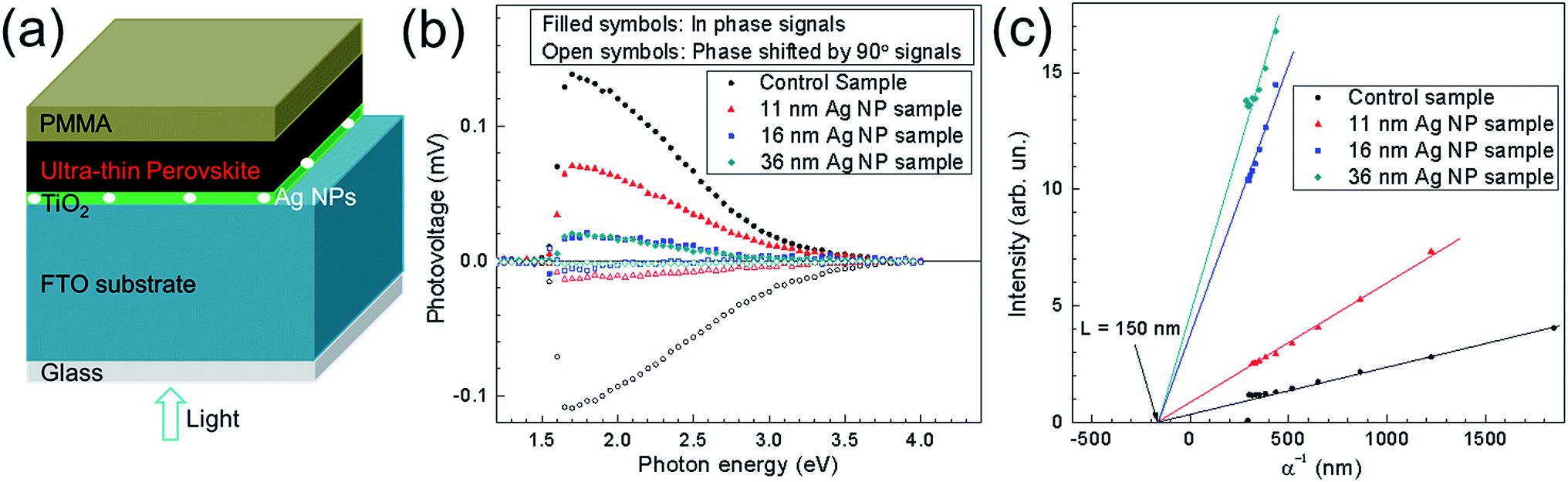 | ||
| Fig. 5 (a) Schematic sample structure of PMMA/ultra-thin perovskite layer/TiO2/Ag NPs/FTO/glass. (b) SPV spectra of the in-phase (filled symbols) and phase shifted by 90° (open symbols) SPV signals of ultra-thin perovskite layers deposited on TiO2/(with and without) Ag NPs/FTO/glass and coated with PMMA. (c) Goodman plots measured for constant SPV signals of ultra-thin perovskite layers deposited on TiO2/(with and without) Ag NPs/FTO/glass and coated with PMMA. | ||
Fig. 5c shows the transport lengths of minority charge carriers in the control sample, 11 nm, 16 nm and 36 nm Ag NP samples derived from SPV.37 For all four samples, the transport lengths are around 150 nm. This means: (1) the appearing surface particles do not influence the transport length of minority charge carriers and (2) the implementation of Ag NPs will not cause reduction of Jsc originating from reduced diffusion lengths of charge carriers.
To further study the effect of Ag NPs on photocurrent enhancement, steady-state PL was measured for the control sample and the 11 nm, 16 nm and 36 nm Ag NP samples. There were no spiro-OMeTAD layer and Au back contact layer for the samples used in PL measurement. The schematic structure of the samples used for PL measurements is shown in Fig. 6a. Lasers with wavelengths of 362 nm and 504 nm were chosen to incident from the glass side for the measurement at CH3NH3PbI3/TiO2 interface and at a deeper position within the CH3NH3PbI3 layer, respectively. The results are shown in Fig. 6b and c. It is observed from Fig. 6b that there is clear quenching of steady-state PL caused by Ag NPs, indicating improved charge separation at the CH3NH3PbI3/TiO2 interface and more electrons being trapped into the TiO2 layer. Correlating this to the above discussion, this can be partly due to the localized surface plasmon resonance (LSPR) of the Ag NPs. The quenching effect becomes stronger with increase of Ag NPs' sizes from 11 nm to 36 nm. Using a laser with a wavelength of 504 nm corresponds to a deeper probing position within the perovskite layer. The effect of PL quenching is significant for the 36 nm Ag NP sample as presented in Fig. 6c, but very slightly for the 11 nm and 16 nm Ag NP samples, respectively. The differences between these three samples are caused by the variation in the particle sizes. The 36 nm Ag NPs are big enough to have an influence on the deeper probing position of the PL, but the 11 nm and 16 nm Ag NPs are too small to have such a clear impact. From the two PL measurements, the consistency on 36 nm Ag NP sample and difference on the 11 nm and 16 nm Ag NP samples confirm that the effect of Ag NPs takes place only very near the Ag NPs. This finding agrees with localization of field enhancement due to the LSP effect. Hence, photocurrent enhancement could be attributed to localized surface plasmon resonances of Ag NPs and the enhanced extraction of electrons into the TiO2 layer.21
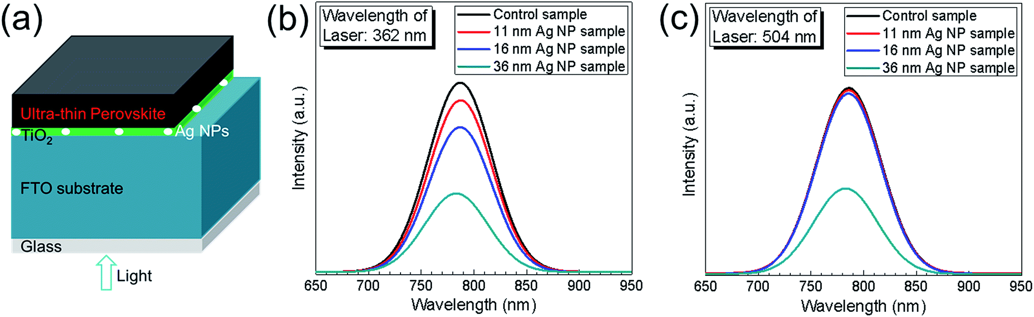 | ||
| Fig. 6 (a) Schematic sample structure of ultra-thin perovskite layer/TiO2/Ag NPs/FTO/glass. (b and c) Photoluminescence spectra of ultra-thin perovskite layers coated on TiO2/FTO/glass (control sample) and on TiO2/Ag NPs/FTO/glass (with different size Ag NPs, i.e., 11 nm, 16 nm and 36 nm) samples. PL spectra at the perovskite/TiO2 interface (b) and at deeper position from interface (c) were measured by laser with wavelengths of 362 nm and 504 nm, respectively. | ||
Fig. 7b shows the EQE for typical devices. Architecture of the devices is presented in Fig. 7a. The EQE spectrum from the 11 nm Ag NP sample and 16 nm Ag NP sample increased in the wavelength range from 350 nm to 700 nm compared to the control sample. The differences on EQE for the three samples indicate the broadband current enhancement by implementation of 11 nm Ag NPs and 16 nm Ag NPs. It has to be mentioned that the photocurrent enhancement shown in EQE spectra is not as significant as 22.2% for the enhancement of the average short-circuit current densities in J–V characteristics (shown in Fig. 2c). The mismatch could be explained by (1) enhancement of photocurrent for the specified samples can be less than the average one and (2) the discrepancy between Jsc measured by EQE and J–V characteristics. Absorption spectra of the control sample and the 11 nm Ag NP and 16 nm Ag NP solar cells are shown in Fig. 7c. It is observed that at wavelengths between 300 nm and 580 nm there is almost no difference for the three devices. At the wavelengths between 580 nm and 700 nm, Ag NPs cause a slight absorption enhancement (in Fig. 7c) which contributes to the EQE improvement. From Fig. 3f, the resonance peak of Ag NPs would be expected at wavelengths around 580 nm. Due to the change of medium surrounding the Ag NPs from air to TiO2, the resonance peak will however redshift which can explain the enhancement between 580 and 700 nm (see, Fig. S5†). Therefore, the resonant behavior of the Ag NPs contributes to the absorption and EQE enhancement of UTPSC in the longer wavelength range. But for shorter wavelength, other effects of the Ag NPs need to cause the enhancement of EQE. Compared to the absorption spectra, there is loss of EQE between 300 nm and 350 nm for all the solar cells. This is because the light is mainly absorbed by FTO substrate and TiO2 layer. It will be very promising if this part of light can also contribute to the performance of UTPSCs.
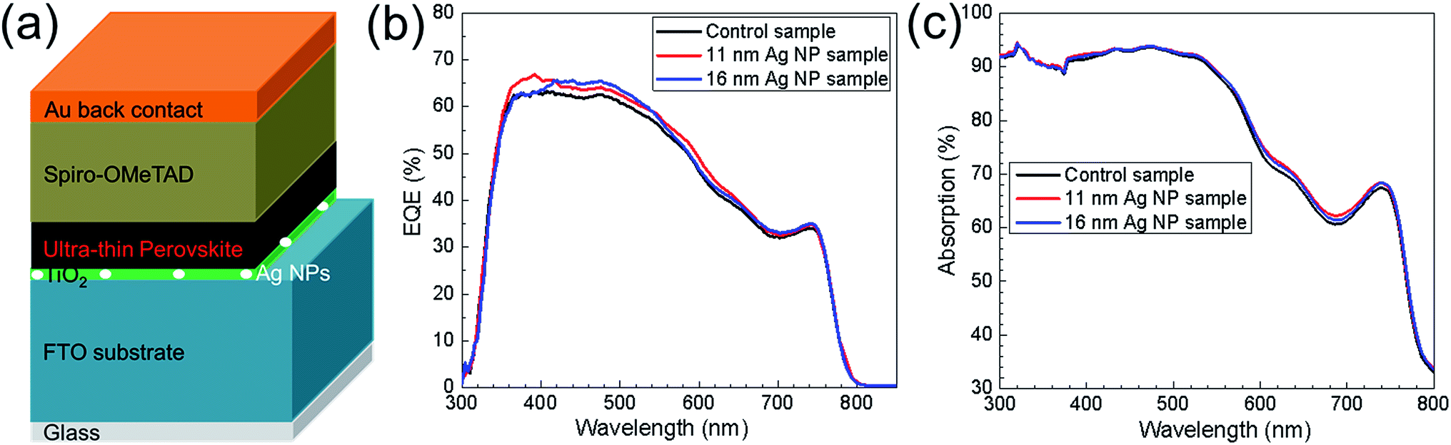 | ||
| Fig. 7 (a) Schematic device structure of ultra-thin perovskite solar cell with incorporation of Ag nanoparticles at the TiO2/FTO interface. (b) EQE of the ultra-thin perovskite solar cells without (control sample), with 11 nm (11 nm Ag NP sample) and with 16 nm (16 nm Ag NP sample) Ag NPs. (c) UV-Vis spectra of the ultra-thin perovskite solar cells without (control sample), with 11 nm (11 nm Ag NP sample) and with 16 nm (16 nm Ag NP sample) Ag NPs. | ||
The results shown above give clear evidences for the encouraging finding that incorporation of Ag NPs into UTPSCs leads to enhancement of both charge separation and diffusion of electrons into TiO2 layer surrounding the Ag NPs which will improve Jsc of UTPSCs. This is very helpful for explaining how Ag NPs improve the performance of UTPSCs and very important for further improving the performance of UTPSCS. As not fully covered Ag NPs can act as recombination centers, electrons which were first trapped in TiO2 de-trap into Ag NPs and hence recombine with holes from the perovskite layer, leading to a decrease of Voc and relatively also Jsc. To overcome this drawback of Ag NPs, increasing the thickness of the TiO2 layer to fully cover the Ag NPs could be one possible way.
Conclusions
In this work, size and density controlled silver nanoparticles were implemented into ultra-thin perovskite solar cells (thickness of perovskite layer is only ∼140 nm) by a low temperature spray chemical vapor deposition method (spray-CVD). This method is easy for large amount production of Ag NPs as well as compatible with the materials which are not able to bear high temperatures. A Jsc enhancement of around 22.2% was observed, as the average Jsc increased from 10.79 mA cm−2 for the control samples to 13.19 mA cm−2 for the samples with 11 nm Ag NPs. This leads to an increase of average PCE from 5.78% to 7.08%, i.e., 22.5% relative. Quenching of steady-state PL indicates that charge separation and trapping of electrons into the TiO2 layer were enhanced at the CH3NH3PbI3/TiO2 interface, which contributed to the enhancement of Jsc. Studies of XPS and SPV show that not fully covered Ag NPs can also work as recombination centers which lead to the decrease of Voc and Jsc. If this problem can be resolved, higher enhancements of Jsc and PCE of UTPSC can be expected. It's also expected that plasmonic Ag NPs can be applied for further improvement of UTPSCs.Acknowledgements
Y. Liu is grateful to the China Scholarship Council for financial support.Notes and references
- H. S. Jung and N.-G. Park, Small, 2015, 11, 10–25 CrossRef CAS PubMed.
- W.-J. Yin, J.-H. Yang, J. Kang, Y. Yan and S.-H. Wei, J. Mater. Chem. A, 2015, 3, 8926–8942 CAS.
- A. Kojima, K. Teshima, Y. Shirai and T. Miyasaka, J. Am. Chem. Soc., 2009, 131, 6050–6051 CrossRef CAS PubMed.
- NREL efficiency chart, http://www.nrel.gov/pv/assets/images/efficiency_chart.jpg, accessed 7th November 2016.
- J.-H. Im, C.-R. Lee, J.-W. Lee, S.-W. Park and N.-G. Park, Nanoscale, 2011, 3, 4088–4093 RSC.
- H.-S. Kim, C.-R. Lee, J.-H. Im, K.-B. Lee, T. Moehl, A. Marchioro, S.-J. Moon, R. Humphry-Baker, J.-H. Yum, J. E. Moser, M. Grätzel and N.-G. Park, Sci. Rep., 2012, 2, 591 Search PubMed.
- M. M. Lee, J. Teuscher, T. Miyasaka, T. N. Murakami and H. J. Snaith, Science, 2012, 338, 643–647 CrossRef CAS PubMed.
- M. Liu, M. B. Johnston and H. J. Snaith, Nature, 2013, 501, 395–398 CrossRef CAS PubMed.
- H. Zhou, Q. Chen, G. Li, S. Luo, T.-b. Song, H.-S. Duan, Z. Hong, J. You, Y. Liu and Y. Yang, Science, 2014, 345, 542–546 CrossRef CAS PubMed.
- Z. Xiao, C. Bi, Y. Shao, Q. Dong, Q. Wang, Y. Yuan, C. Wang, Y. Gao and J. Huang, Energy Environ. Sci., 2014, 7, 2619–2623 CAS.
- E. Della Gaspera, Y. Peng, Q. Hou, L. Spiccia, U. Bach, J. J. Jasieniak and Y.-B. Cheng, Nano Energy, 2015, 13, 249–257 CrossRef CAS.
- L. K. Ono, S. Wang, Y. Kato, S. R. Raga and Y. Qi, Energy Environ. Sci., 2014, 7, 3989–3993 CAS.
- G. E. Eperon, V. M. Burlakov, A. Goriely and H. J. Snaith, ACS Nano, 2014, 8, 591–598 CrossRef CAS PubMed.
- F. Lang, M. A. Gluba, S. Albrecht, J. Rappich, L. Korte, B. Rech and N. H. Nickel, J. Phys. Chem. Lett., 2015, 6, 2745–2750 CrossRef CAS PubMed.
- H. A. Atwater and A. Polman, Nat. Mater., 2010, 9, 205–213 CrossRef CAS PubMed.
- J. A. Schuller, E. S. Barnard, W. Cai, Y. C. Jun, J. S. White and M. L. Brongersma, Nat. Mater., 2010, 9, 193–204 CrossRef CAS PubMed.
- V. E. Ferry, M. A. Verschuuren, H. B. Li, E. Verhagen, R. J. Walters, R. E. Schropp, H. A. Atwater and A. Polman, Opt. Express, 2010, 18, A237–A245 CrossRef CAS PubMed.
- X. Chen, B. Jia, J. K. Saha, B. Cai, N. Stokes, Q. Qiao, Y. Wang, Z. Shi and M. Gu, Nano Lett., 2012, 12, 2187–2192 CrossRef CAS PubMed.
- X. Li, W. C. H. Choy, L. Huo, F. Xie, W. E. I. Sha, B. Ding, X. Guo, Y. Li, J. Hou, J. You and Y. Yang, Adv. Mater., 2012, 24, 3046–3052 CrossRef CAS PubMed.
- G. Yin, A. Steigert, P. Andrae, M. Goebelt, M. Latzel, P. Manley, I. Lauermann, S. Christiansen and M. Schmid, Appl. Surf. Sci., 2015, 355, 800–804 CrossRef CAS.
- Z. Lu, X. Pan, Y. Ma, Y. Li, L. Zheng, D. Zhang, Q. Xu, Z. Chen, S. Wang, B. Qu, F. Liu, Y. Huang, L. Xiao and Q. Gong, RSC Adv., 2015, 5, 11175–11179 RSC.
- M. Qian, M. Li, X.-B. Shi, H. Ma, Z.-K. Wang and L.-S. Liao, J. Mater. Chem. A, 2015, 3, 13533–13539 CAS.
- M. Saliba, W. Zhang, V. M. Burlakov, S. D. Stranks, Y. Sun, J. M. Ball, M. B. Johnston, A. Goriely, U. Wiesner and H. J. Snaith, Adv. Funct. Mater., 2015, 25, 5038–5046 CrossRef CAS.
- Z. Yuan, Z. Wu, S. Bai, Z. Xia, W. Xu, T. Song, H. Wu, L. Xu, J. Si, Y. Jin and B. Sun, Adv. Energy Mater., 2015, 1500038, DOI:10.1002/aenm.201500038.
- H.-L. Hsu, T.-Y. Juang, C.-P. Chen, C.-M. Hsieh, C.-C. Yang, C.-L. Huang and R.-J. Jeng, Sol. Energy Mater. Sol. Cells, 2015, 140, 224–231 CrossRef CAS.
- W. Zhang, M. Saliba, S. D. Stranks, Y. Sun, X. Shi, U. Wiesner and H. J. Snaith, Nano Lett., 2013, 13, 4505–4510 CrossRef CAS PubMed.
- Y. Liu, Y. Fu, T. Dittrich, R. Sáez-Araoz, M. Schmid, V. Hinrichs, M. C. Lux-Steiner and C.-H. Fischer, Thin Solid Films, 2015, 590, 54–59 CrossRef CAS.
- Y. Liu, P. Plate, V. Hinrichs, T. Köhler, M. Song, P. Manley, M. Schmid, P. Bartsch, S. Fiechter, M. C. Lux-Steiner and C.-H. Fischer, J. Nanopart. Res. Search PubMed , submitted.
- K. C. Pingali, D. A. Rockstraw and S. Deng, Aerosol Sci. Technol., 2005, 39, 1010–1014 CrossRef CAS.
- T. C. Pluym, Q. H. Powell, A. S. Gurav, T. L. Ward, T. T. Kodas, L. M. Wang and H. D. Glicksman, J. Aerosol Sci., 1993, 24, 383–392 CrossRef CAS.
- S.-J. Shih and I. C. Chien, Powder Technol., 2013, 237, 436–441 CrossRef CAS.
- N. Kumar, F. Alam and V. Dutta, J. Alloys Compd., 2014, 585, 312–317 CrossRef CAS.
- N. J. Jeon, J. H. Noh, Y. C. Kim, W. S. Yang, S. Ryu and S. I. Seok, Nat. Mater., 2014, 13, 897–903 CrossRef CAS PubMed.
- T. Dittrich, C. Awino, P. Prajongtat, B. Rech and M. C. Lux-Steiner, J. Phys. Chem. C, 2015, 119, 23968–23972 CAS.
- A. Naikaew, P. Prajongtat, M. C. Lux-Steiner, M. Arunchaiya and T. Dittrich, Appl. Phys. Lett., 2015, 106, 232104 CrossRef.
- A. M. Goodman, J. Appl. Phys., 1961, 32, 2550–2552 CrossRef.
- T. Dittrich, F. Lang, O. Shargaieva, J. Rappich, N. H. Nickel, E. Unger and B. Rech, Appl. Phys. Lett., 2016, 109, 073901 CrossRef.
- W. E. I. Sha, X. Ren, L. Chen and W. C. H. Choy, Appl. Phys. Lett., 2015, 106, 221104 CrossRef.
- M. Long, Z. Chen, T. Zhang, Y. Xiao, X. Zeng, J. Chen, K. Yan and J. Xu, Nanoscale, 2016, 8, 6290–6299 RSC.
- M. B. Suwarnkar, R. S. Dhabbe, A. N. Kadam and K. M. Garadkar, Ceram. Int., 2014, 40, 5489–5496 CrossRef CAS.
- M. Harikishore, M. Sandhyarani, K. Venkateswarlu, T. A. Nellaippan and N. Rameshbabu, Procedia Mater. Sci., 2014, 6, 557–566 CrossRef CAS.
Footnote |
| † Electronic supplementary information (ESI) available. See DOI: 10.1039/c6ra25149h |
| This journal is © The Royal Society of Chemistry 2017 |