
 Open Access Article
 This Open Access Article is licensed under a
 Creative Commons Attribution 3.0 Unported Licence
Electromagnetic wave absorption of silicon carbide based materials
Chenyu Liuab,
Dawei Yuc,
Donald W. Kirkb and
Yongjun Xu*a
aSchool of Chemistry and Chemical Engineering, Harbin Institute of Technology, 92 Dazhi Street, Harbin, 150001, China. E-mail: xuyongjun1218@126.com
bDepartment of Chemical Engineering & Applied Chemistry, University of Toronto, 200 College Street, Toronto, Ontario M5S 3E5, Canada
cDepartment of Materials Science and Engineering, University of Toronto, 184 College Street, Suite 140, Toronto, Ontario M5S 3E4, Canada
First published on 3rd January 2017
Abstract
Increasing research effort has been made aiming at developing electromagnetic (EM) wave absorbing materials with high absorption performance. An ideal EM absorber should be relatively light-weight, thermally stable, capable of absorbing wide EM frequency, and cost effective. As a dielectric material, silicon carbide (SiC) has great potential with relatively low density, good thermal and chemical resistance, and it can function at high temperatures or under harsh working environments. This review summarizes the research progress in the design and characterization of SiC and SiC based composites as EM absorption materials. Pristine SiC with various morphological, phase, and structural features can be tailored to achieve better absorption performance. Moreover, SiC based materials can either be modified using dielectric or magnetic materials, or be designed with variation in geometry, composition, and mass fraction of the filler composition for further improvement in EM absorption. This review intends to inspire new concepts and approaches for designing excellent EM absorbing materials.
1. Introduction
The extensive use of electronic equipment and wireless devices such as mobile phones, local area networks and satellite broadcast systems were found to perturb their surroundings and cause pollution in the form of radiated EM signals.1–5 Moreover, electromagnetic interference can weaken biological immune systems, break DNA strands, promote cancers, and present a threat to human health.6–8 EM wave absorbing materials thus have attracted worldwide attention and are widely found in commercial, industrial and military applications.9–12 EM absorbers can reduce EM radiation and improve EM interference shielding by effectively absorbing EM waves and converting them into other kinds of energy such as thermal energy.13,14The EM absorption performance is generally associated with two aspects: (1) the incident EM waves can be transmitted into the materials with minimal reflection on the surface, which requires impedance matching between the material surface and the free space within the material. The impedance matching can be realized using the linkage between the complex relative permittivity and permeability; (2) the incident EM waves can be converted to other forms of energy, in which case strong magnetism or specific electrical properties of the material are required. The ideal EM absorbers should be relatively light-weight, highly thermally stable, capable of absorbing wide EM frequency, and cost effective.15 To meet these stringent requirements, extensive global research efforts have been made to develop new EM wave absorbing materials with excellent EM absorption performance. Absorbers made of various materials have been fabricated in the last few years such as carbon and conductive polymer.16–25 Unfortunately, carbon materials usually have extremely high permittivity and low permeability, resulting in their difficulty in achieving impedance matching. Individual conductive polymer materials mostly need strict preparation requirement and their absorption bandwidth is usually narrow. Moreover, the thermal and chemical resistance of carbon materials and conductive polymer materials at high temperatures and/or under harsh working environments is unsatisfactory which limits their broader applications.
SiC stands out for its unique properties in terms of EM wave absorption. SiC is a dielectric absorber by means of its intrinsic electric dipolar polarization. Furthermore, it can be applied in harsh working environments with good EM absorption performance due to its low thermal expansion, good thermal shock resistance, high strength and good chemical inertness.26,27 Specific morphological and desirable structures have been reported and these could be used to enhance EM wave absorption.28–31 The SiC materials can be in the forms of wire, whisker, fibre, tube, and porous SiC, etc. For example, it has been reported that SiC materials engineered with stacking faults and stacking planes produced extensive polarization under EM irradiation, transforming its energy into heat.14 Also, surface modification of SiC with other dielectric or magnetic materials can introduce multiple polarizations and increase dielectric properties to improve EM absorption performance.32–35 EM absorbers are generally classified into two categories: dielectric and magnetic, based on their primary EM absorption mechanism.7 Combination of these two types of absorbers can enhance EM wave absorption performance by achieving a balance between permeability and permittivity.36–42 As a typical dielectric absorber, SiC can be decorated by magnetic absorbers such as metal particles (e.g. Fe, Co, and Ni), or their metallic oxides to meet the impedance matching.
In this review, we present the EM wave absorption theory, introduce a classification system of EM absorbers, and most importantly, summarize the research efforts and overall progress in utilizing and modifying SiC materials for the application of EM absorption. By doing so, the goal of this review is to inspire new concepts for designing light weight, highly thermally stable EM absorbers with high EM wave absorption performance and wide absorption frequency band.
2. Electromagnetic wave absorption theory
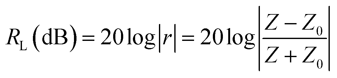
As shown in Fig. 1, the incident EM waves are divided into three parts: reflected waves, transmitted waves and absorbed waves. A scenario is considered here, in which the EM waves are incident on the surface of an absorber with complex permittivity ε (εr = ε′ − jε′′) and permeability μ (μr = μ′ − jμ′′), and the absorber is surrounded by free space. According to the well-known theory for describing the propagation of EM waves, i.e. Maxwell's equations, EM wave absorption performance is basically estimated by reflection loss (RL). RL can be calculated using the following equations:
Z = Z0(μr/εr)1/2![[thin space (1/6-em)]](https://www.rsc.org/images/entities/char_2009.gif) tanh[j(2πfd/c)(μrεr)1/2] tanh[j(2πfd/c)(μrεr)1/2]
| (1) |
 | (2) |
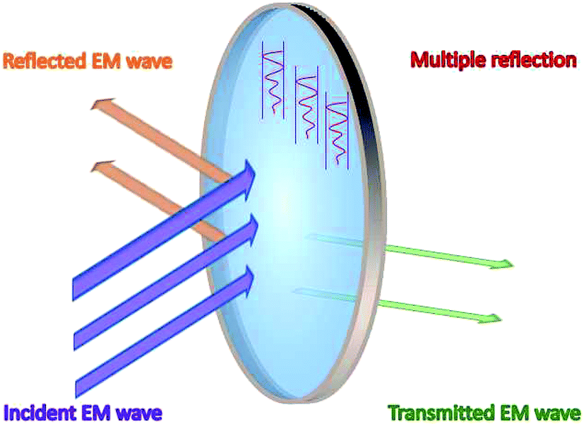 | ||
| Fig. 1 Schematic of the incident EM waves through an EM absorber. | ||
When EM waves are obliquely incident to the surface, the incidence angle is not zero. It is known that the reflection coefficient can be influenced by not only the angle of the incidence EM waves, but also by polarization of the material. The reflection coefficient can be represented by eqn (3) and (4).
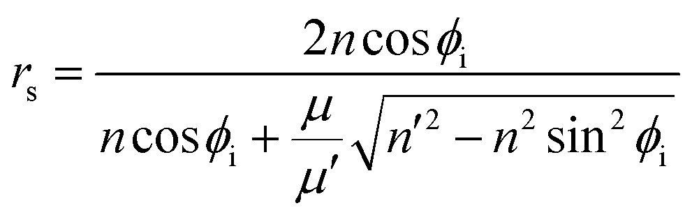 | (3) |
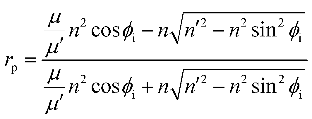 | (4) |
Other than impedance matching, high dielectric and/or magnetic loss also need to be considered in order to achieve high EM absorption performance. The transmitted EM wave must be absorbed, and its energy dissipated in the form of heat. This requires high dielectric or magnetic losses, which are determined by the complex permittivity (εr = ε′ − jε′′) and permeability (μr = μ′ − jμ′′), respectively. The real parts (ε′ and μ′) of the complex permittivity and permeability represent the storage capability of the electric and magnetic energy. The imaginary parts (ε′′ and μ′′) represent the loss capability of electric and magnetic energy. So it is necessary to design an absorber with either high dielectric loss or magnetic loss and with the capability of impedance matching.
3. Classification of electromagnetic wave absorption materials
EM absorbers are generally classified into two categories: dielectric and magnetic absorbers. Mechanisms of EM loss in the absorbers can be classified into dielectric loss, magnetic loss, eddy current loss, residual loss, resonance loss, and so on. It is commonly reported that several of the above-mentioned mechanisms were integrated in one type of material to enhance the absorption performance and broaden the absorption frequency. In this review, EM wave absorption materials will be categorized into four types based on the structure of the absorbers.The first type is produced by mechanically mixing the dielectric and magnetic materials together. Fig. 2a presents the schematic illustration of the structure of the absorber. There is no chemical reaction taking place or chemical bonding between these two materials during its preparation.
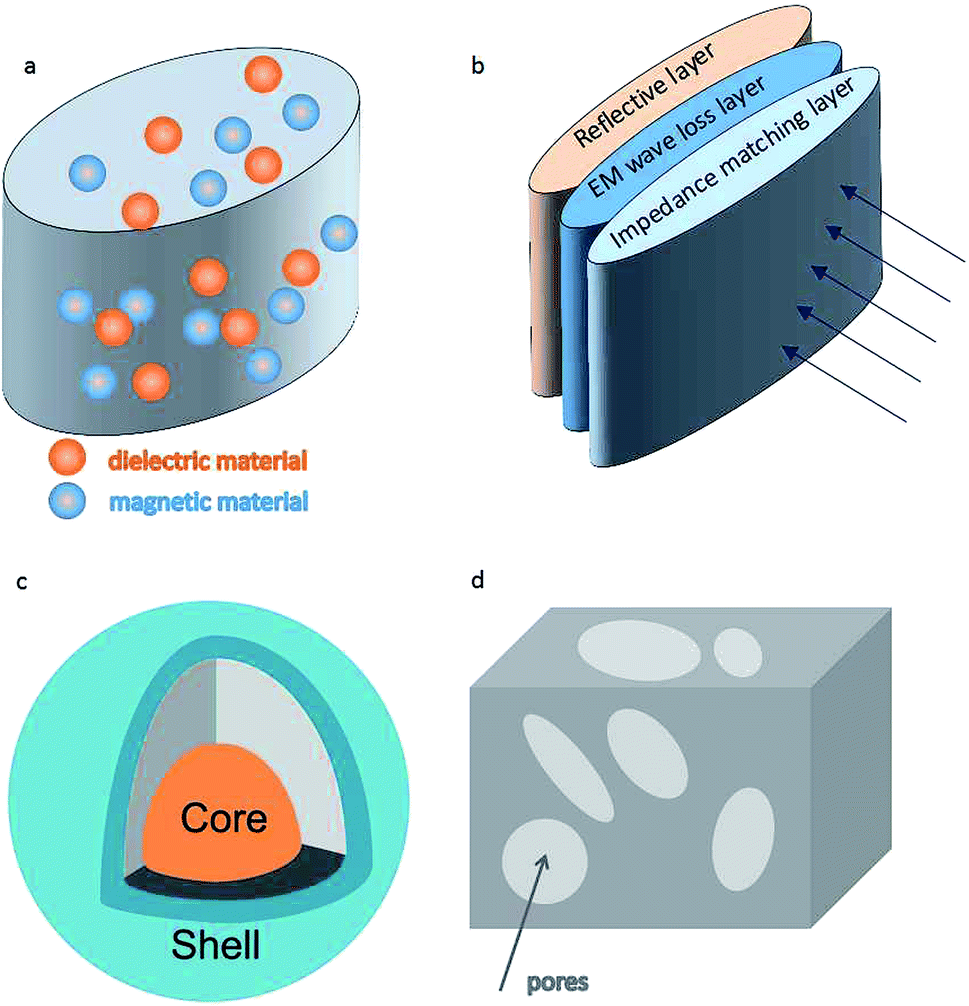 | ||
| Fig. 2 Schematics of possible structures for the four types of EM wave absorbers. | ||
The second type is named as multilayer structure absorber.43,44 The basic structure is composed of three layers: an impedance matching layer; an attenuation layer; and a reflective layer (Fig. 2b). With the help of an impedance matching layer on the surface, the incident EM waves can be easily transmitted into the absorber with minimal reflection. The transmitted waves then will be absorbed by the attenuation layer through the mechanism of high dielectric or magnetic loss. The third layer (usually made of metal) is highly reflective. If some incident waves pass through the first and second layers, they will be reflected by the inner reflective layer, and have to pass through the attenuation layer again.
The third type is hierarchical hybrids with specific morphologies and desirable combinations of the dielectric and magnetic materials.45–56 The chemical bonding and interfacial effect present among the components in the hybrid induce charge redistribution and generates multiple interfacial polarizations, which attenuates the transmitted EM wave. A core–shell structure (Fig. 2c) was selected to represent this type of absorber. Nano-sized materials are generally applied in this type of absorber.57,58 This is because nano sized materials show prominent electric, magnetic, and optic properties, such as having large specific surface area and high eddy current loss. These properties are beneficial for improving the EM absorption ability and broadening the absorption frequencies.
The fourth type is a low density absorber, which is characterized by its porous or hollow structure.59–63 In addition to its low density, the special structure is also beneficial for EM wave absorption. When an incident wave enters into the pores of a porous absorber (Fig. 2d), it interacts with the surface of the pores, resulting in its first absorption. The remainder of the wave gets further absorbed during its sequential multiple reflection/absorptions within additional pores. The multiple reflections at the interior of the pores improves absorption performance to a large extent. The multiple reflections also efficiently increase the effective surface area and path length, resulting in a reduced size of absorber.
It is not easy for simple materials with single dielectric or magnetic properties to possess high performance in EM attenuation. Therefore, proper design of absorbers must include impedance matching and possession of high dielectric loss or magnetic loss. The components and structures of an absorber have extensive opportunities for design. Blends of various dielectric or magnetic materials and the combination of several of the four types could potentially lead to significant improvement in the EM absorption performance.
4. EM wave absorption performance of pristine SiC materials
4.1. Effects of morphological and phase change of SiC
Morphology of SiC materials can be classified based on the number of structural dimensions. It can be 0D (e.g. nano crystals or particles), 1D (e.g. wires, tubes, and whiskers), 2D (e.g. flakes, platelets), and 3D (e.g. more complex structures). SiC is a covalently bonded IV–IV compound that each Si/C atom is surrounded by four C/Si atoms in strong tetrahedral sp3-hybridized bonds, resulting in its good chemical and thermal resistance.64 The crystallographic structure of SiC consists of closely packed Si–C double layers.64 Different crystallographic forms (named polytypes) can be caused by different stacking sequences of C–Si double layers within one period.64 There are more than 250 polytypes but only some most common polytypes have been investigated at great depth.64–67 The polytypes and dimensions of SiC play an important role in determining the physical properties of SiC, such as its electrical and thermal properties as well as influencing its EM absorption ability.68–78Zhang14 investigated β-SiC nanowires with different stacking fault populations and stacking planes which was fabricated by simply varying the heating temperature. SiC nanowires with a higher carbon unoccupied density of states (DOS) has a higher stacking fault content, which leads to a greater population of dipoles. The reorientation of the dipoles can cause significant polarization and energy attenuation. Fig. 3 presents the relationships among the carbon unoccupied DOS, stacking fault content and RL values. The lowest reflection loss of −30 dB with a broad absorption band of 3.7 GHz was achieved using the SiC nanowires fabricated at 1400 °C. Aïssa79 studied amorphous silicon carbide (α-SiC) in terms of its EM wave absorption and microwave heating performance. Amorphous hydrogenated silicon carbide (α-SiC:H) thin film was deposited on [100] un-doped silicon substrates with a thickness of 1 μm by plasma enhanced chemical vapour deposition technology. The absorber shows a remarkable absorption performance such that more than 96% of the incident EM waves were attenuated. Furthermore, two-wavelength pyrometer measurements indicated that the EM energy was converted to thermal energy. A temperature higher than 2000 K could be achieved in less than 100 s exposure under EM irradiation.
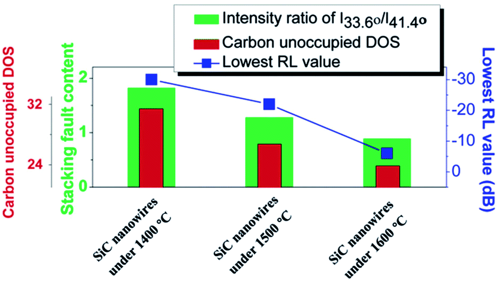 | ||
| Fig. 3 Relationships among the carbon unoccupied DOS, stacking fault content and RL values. Reproduced from ref. 14 with permission from the Royal Society of Chemistry. Copyright 2015. | ||
4.2. Effects of structural changes of SiC
Special structures of SiC materials such as porous and hollow structures were proposed to improve absorption capacity.80–83 The special structure increases specific inner surface areas which results in subsequent multi-reflection of the incident EM waves. It is also an effective way of making the absorbers light-weight by introducing porous and hollow structures within the materials. Our research group84 reported a porous SiC material which incorporated natural porous structure of the apple fruit to demonstrate excellent EM absorption performance. SEM images of the porous SiC are shown in Fig. 4a. Higher magnification images Fig. 4b and c illustrate the SiC fibres were grown in situ on the porous apple framework and the highly populated stacking faults present in the apple fibres, respectively. The stacking faults within the SiC can improve electric charge redistribution, and generate extensive polarizations, resulting in energy dissipation. The authors concluded that a porous material is advantageous for reaching impedance matching due to its lower permittivity than non-porous materials. Moreover, the cellular, interconnected and well-organized 3D network porous structure was able to cause multi-reflection of EM waves within the absorber, resulting in the outstanding absorption performance. As a result, dissipation of EM waves is very efficient due to the multi-reflection mechanism. Fig. 4d indicates that the lowest reflection loss of SiC porous materials is −60 dB. It showed an excellent absorption performance (RL < −10 dB) at a high frequency range from 14 to 18 GHz (shown in Fig. 4e).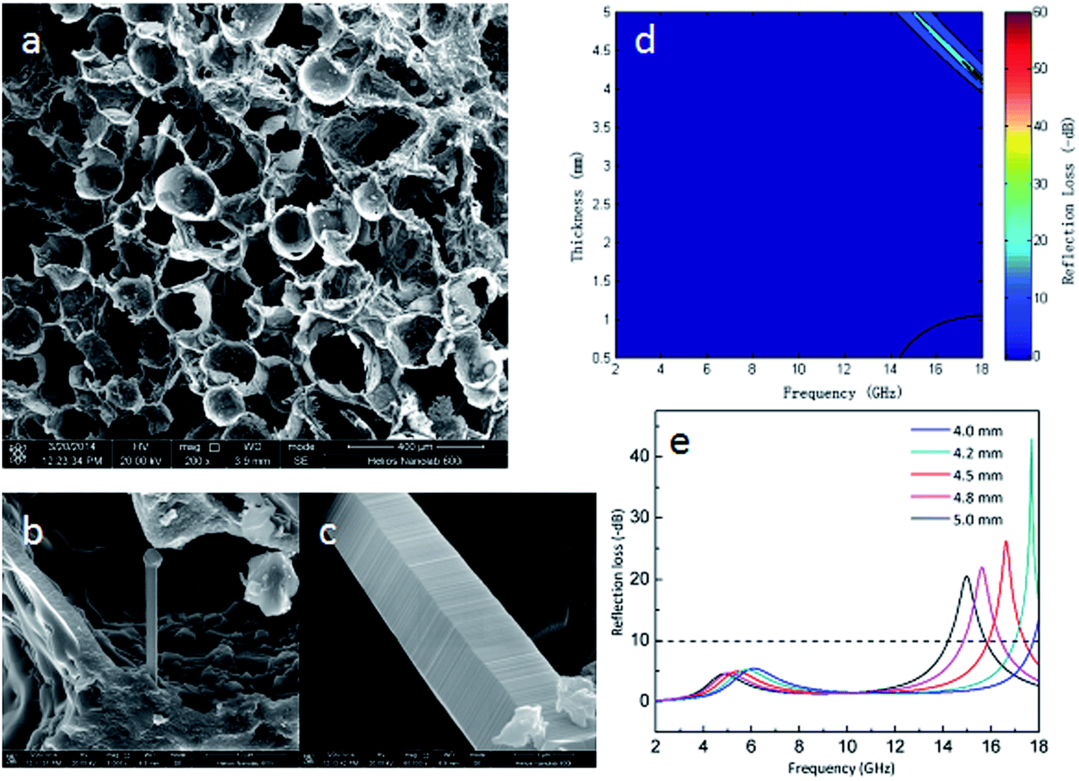 | ||
| Fig. 4 (a–c) SEM images of porous SiC at various magnifications; (d) EM wave absorption characteristics of the porous SiC; (e) optimal reflection loss spectra plotted against the frequency of porous SiC with various thickness. Reproduced from ref. 84 with permission from the Royal Society of Chemistry. Copyright 2016. | ||
Even though the SiC absorbers mentioned above are pristine materials, their impedance matching and strong dielectric loss can be achieved through adjustment of their morphology and structure. The dielectric property of SiC can be greatly influenced by specific structure of absorbers, type of polytypes, content of stacking faults, and density of unoccupied states. Furthermore, pristine SiC materials are both thermal and chemical resistant, which makes it possible to function under harsh working environments.
5. EM wave absorption performance of modified SiC materials
As discussed above, SiC with various structures and morphologies already possesses good EM wave absorption capability. But for practical application, its dielectric property is relatively poor due to its single polarization (intrinsic electric dipolar polarization) and low conductivity. Therefore, in order to improve dielectric permittivity of SiC, introduction of multiple polarizations and enhancement of conductivity are required. Surface decoration, doping, or forming composites with other materials have been considered as effective ways to allow impedance matching, enhancing EM absorption, and broadening the EM absorption frequencies.5.1. Modification of SiC using dielectric materials
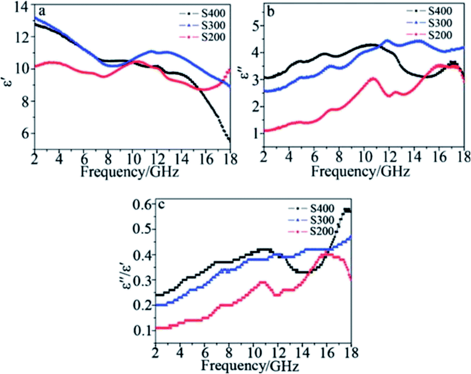
The dielectric materials used for chemical modification can be carbon based materials such as CNT, carbon black, graphene, and organic polymeric materials, for instance PANI, PVDF, or inorganic materials such as Si3N4, SiO2.81,85–110 Zhu26 fabricated MWCNT/SiC porous nanocomposites with reaction temperatures of 200, 300 and 400 °C designated as S200, S300 and S400, respectively. Fig. 5 shows the EM wave absorption characteristics of the samples. More than 99% absorption was achieved in the range of 10.6–18 GHz with a thickness of 1.6–2.2 mm. The authors claimed that the reason for its outstanding absorption is due to the enhanced dielectric loss ascribed to intensive polarization. The polarization is caused by mainly four factors: synergistic effects among the high density of defects in the etched MWCNTs (pores, lattice distortions or dangling bonds); interfacial polarization between MWCNTs and SiC, stacking faults in the SiC crystallites and grain boundaries in the polarized SiC nanoparticles; porous structure of the composites. Furthermore, as was mentioned before, dielectric loss is represented by the relative complex permittivity. The real part ε′ and image part ε′′ stands for storage and loss capability of the EM energy, respectively. From Fig. 6, it is apparent that both ε′′ and dielectric loss tangent tgδE = ε′′/ε′ increases gradually for the three composites with the increasing sequence of S200, S300 and S400. As a result, MWCNT/SiC porous nanocomposites obtained at 400 °C achieved the best absorption performance.
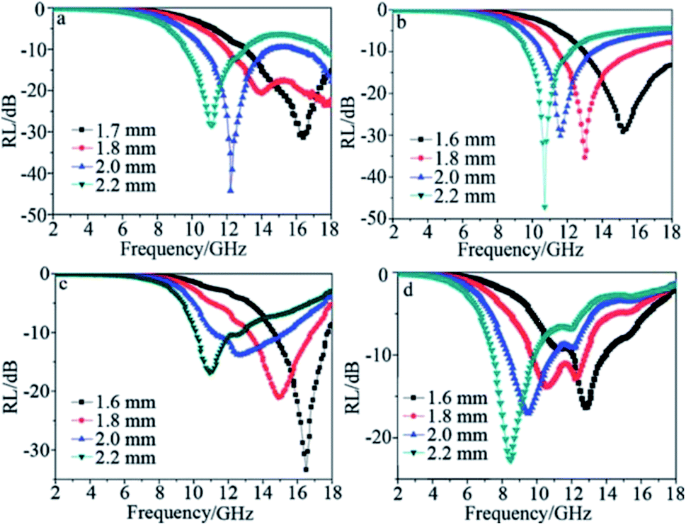 | ||
| Fig. 5 EM wave absorption of the MWCNT/SiC porous composites: (a) S400, (b) S300, (c) S200 and (d) MWCNTs. Reproduced from ref. 26 with permission from the Royal Society of Chemistry. Copyright 2011. | ||
 | ||
| Fig. 6 Permittivity characterization of the samples in the 2–18 GHz range: (a) real part and (b) imaginary part of complex permittivity and (c) dielectric loss tangent. Reproduced from ref. 26 with permission from the Royal Society of Chemistry. Copyright 2011. | ||
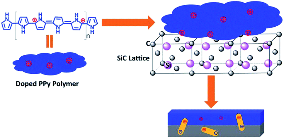
Zhang111 developed a novel method for fabricating core–shell PPy/SiC nanocomposites by in situ self-assemble and growing PPy nano-films on SiC nanowires. As is known PPy is polymerized through oxidation that possesses an abundance of positive bipolarons. In the PPy/SiC hybrids, the oxidation-polymerized and doped PPy chains self-assembled into positive nanoparticles on the surface of SiC as a coating layer. Defect dipoles were produced after these positive nanoparticles moved close to the SiC lattice, resulting in the enhancement of polarizations and conductivity. Fig. 7 presents the polarization model of dielectric relaxations in the as-prepared PPy/SiC hybrids. The effective EM absorption bandwidth covered 6.52 GHz (10.52–17.04 GHz) with a thickness of 2.5 mm.
 | ||
| Fig. 7 Scheme of the induced polarization model for PPy/SiC hybrid. Reproduced from ref. 111 with permission from the Royal Society of Chemistry. Copyright 2016. | ||
In summary, proper decoration of SiC with highly conductive materials can enhance dielectric loss of the material without preventing the impedance matching, resulting in a higher performance of EM absorption. It can also be advantageous to select a conductive material with special properties (e.g. defects and bipolarons as discussed above) and can interact with the SiC component.
5.2. Modification of SiC using magnetic materials
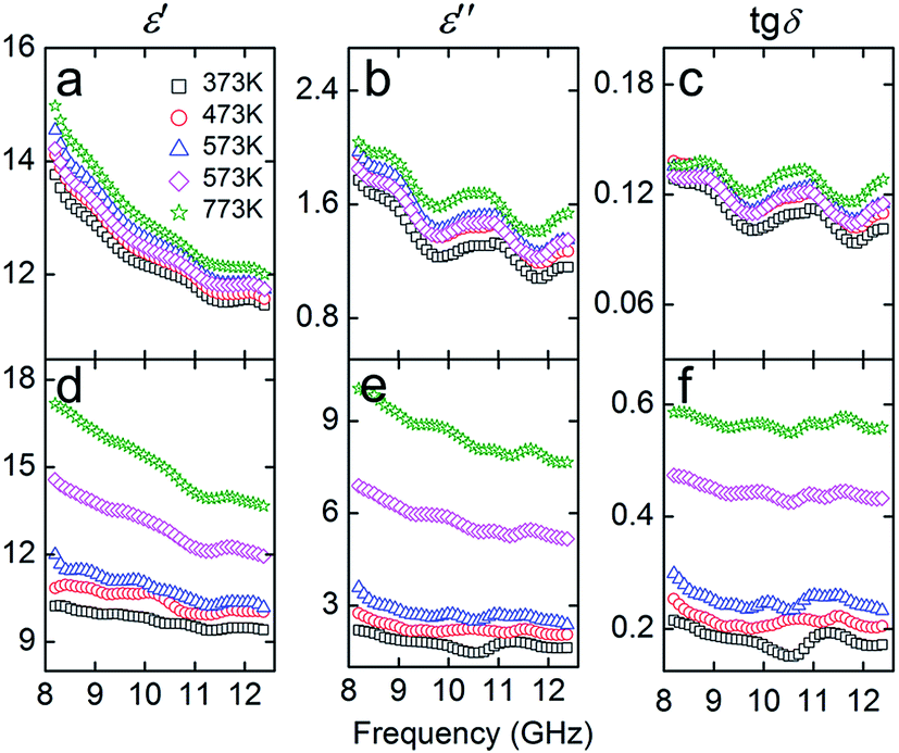
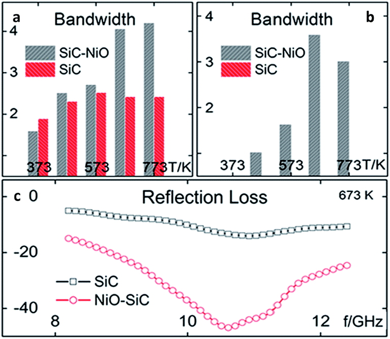
Magnetic materials (metals or their individual oxides) can also be used for the modification of SiC, such as Fe, Co, Ni.83,88,112–122 Yang123,124 prepared a hierarchical structure of NiO nanorings on SiC. The NiO nanorings significantly improved the dielectric properties of SiC. Fig. 8 illustrates dielectric properties of NiO–SiC and pure SiC. When measured under the same temperatures, NiO–SiC has an imaginary part of permittivity ε′′ which is significantly higher than that of SiC. The maximum dielectric loss tangent (tgδ) of NiO–SiC is almost five times larger than that of SiC at a temperature of 773 K. Fig. 9 reveals absorption bandwidth and reflection loss values of NiO–SiC and SiC. The absorption bandwidth of NiO–SiC is obviously broader than that of SiC. At elevated temperatures, the EM wave absorption performance of NiO–SiC reached as low as −50 dB. Sun125 used a scale-up double-hydrolysis reaction method to grow ZnO nanocrystals on the SiC nanowires. The dielectric properties were greatly enhanced and the minimum reflection loss reached −42.11 dB with a loading of 30 wt% and a thickness of 3.5 mm. The effective EM absorption bandwidth covered 6.6 GHz (11.08–17.68 GHz) with a thickness of 2.5 mm.
 | ||
| Fig. 8 Complex permittivity and loss tangent versus frequency of (a–c) SiC and (d–f) NiO–SiC. Reproduced from ref. 123 with permission from the ACS Publications. Copyright 2015. | ||
 | ||
| Fig. 9 Absorption bandwidth of NiO–SiC and SiC at different temperatures at the level of (a) −10 dB and (b) −20 dB; (c) reflection loss value of NiO–SiC and SiC versus frequency (T = 673 K). Reproduced from ref. 123 with permission from the ACS Publications. Copyright 2015. | ||
As discussed in Section 2., both dielectric loss and magnetic loss contribute to the EM absorption performance. As a typical dielectric absorber, pristine SiC is diamagnetic. The magnetic loss of SiC has almost no effect on the overall absorption. In order to obtain magnetism, SiC can be doped with magnetic materials.32,126,127 When the combination of relative permittivity and permeability are realized, the materials should possess an excellent EM absorption performance. Liang33 fabricated SiC–Fe3O4 hybrid nanowires with a core–shell structure. The coverage of Fe3O4 nanoparticles is able to be adjusted simply by changing the mass ratio of the precursors. Fig. 10a illustrates that after coating with Fe3O4 nanoparticles, the dielectric loss tangent of all the SiC–Fe3O4 hybrid samples increased, with the highest values appearing when mass ratio of the precursors was between 1:4 and 1:6. Fig. 10b shows the magnetic loss tangent of the samples. As a dielectric material, SiC has zero magnetic loss (not shown). The SiC–Fe3O4 hybrid nanowires showed high magnetic loss tangent values, which means the introduced magnetic material significantly enhanced the complex permeability of the absorber. Fig. 11 presents reflection losses of SiC and SiC–Fe3O4 hybrid samples. The absorption performance was significantly improved after the incorporation of Fe3O4 nanoparticles. The authors claimed that apart from multi-interfaces within the core–shell structure and synergistic interactions between SiC and Fe3O4 nanoparticles, this improvement of absorption performance can also be attributed to the resonance in complex permittivity and permeability caused by the introduction of Fe3O4 nanoparticles, resulting in significantly enhanced magnetic loss and achieving better impedance matching.
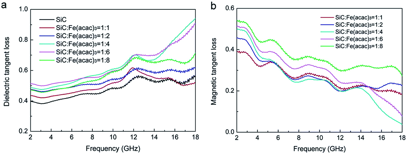 | ||
| Fig. 10 (a) The dielectric loss tangent and (b) the magnetic loss tangent of SiC–Fe3O4 hybrids obtained at different weight ratios of SiC:Fe(acac)3. Reproduced from ref. 33 with permission from the Royal Society of Chemistry. Copyright 2014. | ||
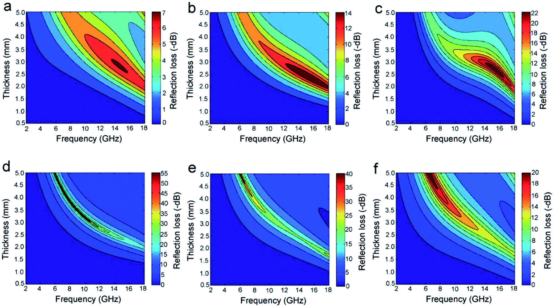 | ||
| Fig. 11 Reflection loss values of (a) SiC nanowires and SiC–Fe3O4 hybrids synthesized at ratios of SiC:Fe(acac)3 being (b) 1:1, (c) 1:2, (d) 1:4, (e) 1:6, and (f) 1:8 from. Reproduced from ref. 33 with permission from the Royal Society of Chemistry. Copyright 2014. | ||
Xie128 used a novel method to fabricate carbon coated Co–SiC nanocomposites. The Co was in situ converted from Co3O4 on the surface of SiC, and then followed by coating with carbon. As can be seen from Fig. 12, when Co–SiC nanocomposites were coated with carbon, both ε′ and ε′′ increased dramatically compared with those of Co–SiC and SiC samples. The values of μ′ and μ′′ for SiC are around 1 and 0, respectively, meaning no magnetic loss. The value of μ′ increased after magnetic material Co was introduced into the material, and was reduced slightly after the coating of carbon. Compared with the fluctuation of μ′, there is little variation for μ′′. The combination of SiC, Co, and carbon effectively realized a better matching between the complex permittivity and permeability. As a result, the carbon coated Co–SiC nanocomposites exhibited a high EM absorption performance with a broad absorption bandwidth. Liang85 synthesized SiC/Co/SiO2 material of multi-shell structure with a broad absorption bandwidth from 9.1 to 18 GHz (RL < −10 dB). The SiO2 shell introduced charge transfer between SiO2 and Co to achieve the impedance matching, resulting in promotion of the incident EM waves entering into the absorber. Subsequently, the EM waves were effectively absorbed due to the strong interfacial polarization and associated relaxation within the SiC/Co/SiO2 nanowire material.
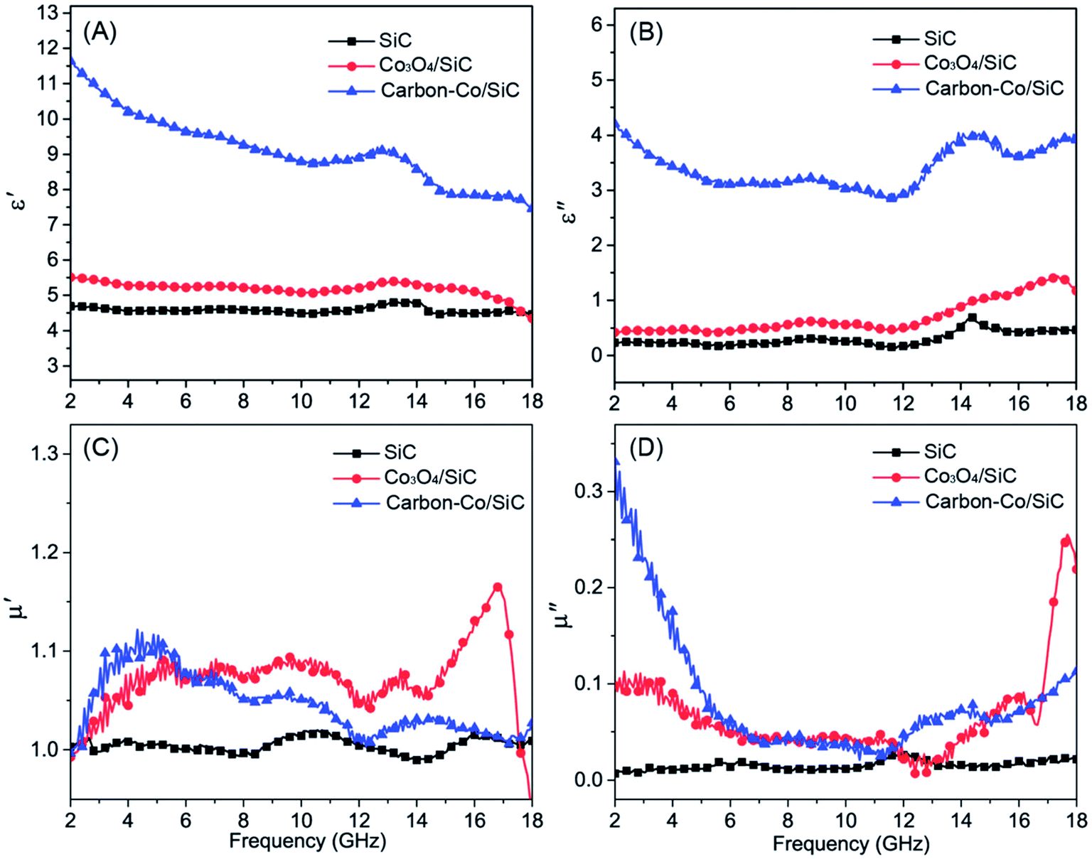 | ||
| Fig. 12 Permittivity and permeability characterization of the prepared samples in the 2–18 GHz range: (A) real part and (B) imaginary part of complex permittivity spectra and (C) real part and (D) imaginary part of complex permeability spectra. Reproduced from ref. 128 with permission from the Royal Society of Chemistry. Copyright 2013. | ||
Metallic materials with both high conductivity and magnetic property have been used widely in EM absorption applications. They are potential candidates for decoration of dielectric materials to achieve impedance matching and enhance dielectric and magnetic loss to improve EM absorption.
6. Conclusions and prospects
6.1. Conclusions
As a dielectric material, SiC has good thermal and chemical resistance at high temperatures and/or under harsh working environments, which makes it an attractive candidate for ideal EM wave absorption. Its dielectric loss is relatively low due to its single intrinsic electric dipolar polarization and it has low electrical conductivity which limits the possibility for its broader applications. This weakness can be partially solved by tailoring the morphological, phase, or structural features of pristine SiC to enhance its polarization and multi-reflection of the incident EM waves. This can be achieved by, for example, inducing greater population of dipoles and by increasing specific inner surface areas, respectively. Surface decoration, doping, and making composites with other materials have proven to be effective strategies to further improve the dielectric permittivity of SiC by the introduction of multiple polarizations and enhancement of conductivity. In this review it was shown that SiC can be modified by carbon based materials (e.g. CNT, carbon black, graphene), organic polymeric materials, (e.g. PANI, PVDF), inorganic materials (e.g. Si3N4, SiO2), and metal materials (e.g. Fe, Co, Ni or their individual oxides). The three most important parameters, dielectric loss, magnetic loss and impedance matching were discussed according to absorption theory. Manipulation of these three parameters on SiC based materials by surface, structural, or compositional modification was presented.6.2. Prospects
More research effort is still required to design SiC and SiC based materials for the application of EM absorption. Generally, the methods for synthesizing SiC in EM absorption field are lack of enough investigation from thermodynamics and kinetics points of view. For example, more attention should be paid to the growth behavior of SiC such as nucleation, growth and its functionalization. The morphology, phase and structure of SiC can therefore be controlled better for further improvement in EM absorption performance. Computational modelling integrated with thermodynamic calculation and experimentation could be an attemptable way. On the other hand, there is a need to advance the development of modification techniques to achieve quantitative modification and enhance the binding force between the components in the case of composites. Furthermore, it is believed that mechanical and physical properties of the absorber are extremely important for broader applications, and more efforts should be devoted to this aspect.Deeper insights into the mechanisms of EM wave absorption by SiC and SiC based materials will be revealed along with the ongoing research efforts. There is no doubt that SiC and SiC based materials have extensive room for investigation and will make a more significant contribution in the application of EM absorption in the future.
Acknowledgements
The authors are deeply thankful for the financial support of the National High Technology Research and Development Program 863 (2007AA03Z337). The authors would like to appreciate the financial support from Daqing Petroleum Administration Bureau. The authors would also like to thank the China Scholarship Council (CSC, No. 201606120236) for providing the financial support.Notes and references
- B. Zhao, G. Shao, B. Fan, W. Zhao and R. Zhang, Phys. Chem. Chem. Phys., 2015, 17, 2531–2539 RSC.
- X. M. Meng, X. J. Zhang, C. Lu, Y. F. Pan and G. S. Wang, J. Mater. Chem. A, 2014, 2, 18725–18730 CAS.
- N. Li, M. Cao and C. Hu, J. Mater. Chem., 2012, 22, 18426 RSC.
- N. Joseph, J. Varghese and M. T. Sebastian, J. Mater. Chem. C, 2016, 4, 999–1008 RSC.
- A. Xie, W. Jiang, F. Wu, X. Dai, M. Sun, Y. Wang and M. Wang, J. Appl. Phys., 2015, 118, 204105 CrossRef.
- R. Girgert, C. Grundker, G. Emons and V. Hanf, Bioelectromagnetics, 2008, 29, 169–176 CrossRef CAS PubMed.
- C. Liu, Y. Xu, L. Wu, Z. Jiang, B. Shen and Z. Wang, J. Mater. Chem. A, 2015, 3, 10566–10572 CAS.
- J. R. Jauchem, K. L. Ryan and M. R. Frei, Bioelectromagnetics, 2000, 21, 159–166 CrossRef CAS PubMed.
- Y. L. Ren, H. Y. Wu, M. M. Lu, Y. J. Chen, C. L. Zhu, P. Gao, M. S. Cao, C. Y. Li and Q. Y. Ouyang, ACS Appl. Mater. Interfaces, 2012, 4, 6436–6442 CAS.
- G. Liu, L. Wang, G. Chen, S. Hua, C. Ge, H. Zhang and R. Wu, J. Alloys Compd., 2012, 514, 183–188 CrossRef CAS.
- G. W. Hanson, R. C. Monreal and S. P. Apell, J. Appl. Phys., 2011, 109, 124306 CrossRef.
- G. S. Wang, X. J. Zhang, Y. Z. Wei, S. He, L. Guo and M. S. Cao, J. Mater. Chem. A, 2013, 1, 7031 CAS.
- P. B. Liu, Y. Huang and X. Sun, ACS Appl. Mater. Interfaces, 2013, 5, 12355–12360 CAS.
- H. Zhang, Y. Xu, J. Zhou, J. Jiao, Y. Chen, H. Wang, C. Liu, Z. Jiang and Z. Wang, J. Mater. Chem. C, 2015, 3, 4416–4423 RSC.
- Y. Ren, C. Zhu, S. Zhang, C. Li, Y. Chen, P. Gao, P. Yang and Q. Ouyang, Nanoscale, 2013, 5, 12296–12303 RSC.
- M. S. Cao, J. Yang, W. L. Song, D. Q. Zhang, B. Wen, H. B. Jin, Z. L. Hou and J. Yuan, ACS Appl. Mater. Interfaces, 2012, 4, 6948–6955 Search PubMed.
- L. Kong, X. W. Yin, X. Y. Yuan, Y. J. Zhang, X. M. Liu, L. F. Cheng and L. T. Zhang, Carbon, 2014, 73, 185–193 CrossRef CAS.
- Z. Liu, J. Wang, D. H. Xie and G. Chen, Small, 2008, 4, 462–466 CrossRef CAS PubMed.
- W. L. Song, M. S. Cao, M. M. Lu, J. Liu, J. Yuan and L. Z. Fan, J. Mater. Chem. C, 2013, 1, 1846–1854 RSC.
- L. Kong, X. W. Yin, Y. J. Zhang, X. Y. Yuan, Q. Li, F. Ye, L. F. Cheng and L. T. Zhang, J. Phys. Chem. C, 2013, 117, 19701–19711 CAS.
- J. H. Li, L. Wang and H. Yu, J. Mater. Sci., 2009, 44, 3917–3927 CrossRef.
- Y. Sun, F. Xiao, X. Liu, C. Feng and C. Jin, RSC Adv., 2013, 3, 22554–22559 RSC.
- H. Wang, J. Y. Feng, X. J. Hu and K. M. Ng, Nanotechnology, 2009, 20, 095601 CrossRef PubMed.
- M. K. Han, X. W. Yin, L. Kong, M. Li, W. Y. Duan, L. T. Zhang and L. F. Cheng, J. Mater. Chem. A, 2014, 2, 16403–16409 CAS.
- Y. X. Gong, L. Zhen, J. T. Jiang, C. Y. Xu, W. S. Wang and W. Z. Shao, CrystEngComm., 2011, 13, 6839–6844 RSC.
- H. L. Zhu, Y. J. Bai, R. Liu, N. Lun, Y. X. Qi, F. D. Han and J. Q. Bi, J. Mater. Chem., 2011, 21, 13581 RSC.
- Y. K. Dou, J. B. Li, X. Y. Fang, H. B. Jin and M. S. Cao, Appl. Phys. Lett., 2014, 104, 052102 CrossRef.
- H. Lv, X. Liang, G. Ji, H. Zhang and Y. Du, ACS Appl. Mater. Interfaces, 2015, 7, 9776–9783 CAS.
- R. Narasimman, S. Vijayan, K. S. Dijith, K. P. Surendran and K. Prabhakaran, Mater. Chem. Phys., 2016, 181, 538–548 CrossRef CAS.
- F. Wu, M. Sun, W. Jiang, K. Zhang, A. Xie, Y. Wang and M. Wang, J. Mater. Chem. C, 2016, 4, 82–88 RSC.
- H. Lv, H. Zhang, B. Zhang, G. Ji, Y. He and Q. Lin, J. Mater. Chem. C, 2016, 4, 5476–5482 RSC.
- H. Wang, L. Wu, J. Jiao, J. Zhou, Y. Xu, H. Zhang, Z. Jiang, B. Shen and Z. Wang, J. Mater. Chem. A, 2015, 3, 6517–6525 CAS.
- C. Liang, C. Liu, H. Wang, L. Wu, Z. Jiang, Y. Xu, B. Shen and Z. Wang, J. Mater. Chem. A, 2014, 2, 16397–16402 CAS.
- W. L. Song, M. S. Cao, M. M. Lu, J. Liu, J. Yuan and L. Z. Fan, J. Mater. Chem. C, 2013, 1, 1846 RSC.
- W. Jiang, M. Sun, K. Zhang, X. Dai, Y. Xia, D. Wang, A. Xie and F. Wu, RSC Adv., 2016, 6, 68128–68133 RSC.
- H. Lv, G. Ji, H. Zhang, M. Li, Z. Zuo, Y. Zhao, B. Zhang, D. Tang and Y. Du, Sci. Rep., 2015, 5, 18249 CrossRef CAS PubMed.
- H. Lv, G. Ji, X. Liang, H. Zhang and Y. Du, J. Mater. Chem. C, 2015, 3, 5056–5064 RSC.
- X. Zhang, Y. Rao, J. Guo and G. Qin, Carbon, 2016, 96, 972–979 CrossRef CAS.
- H. Zhao, Z. Li, N. Zhang, Y. Du and P. Xu, RSC Adv., 2016, 6, 72263–72268 RSC.
- P. Xu, X. J. Han, X. R. Liu, B. Zhang, C. Wang and X. H. Wang, Mater. Chem. Phys., 2009, 114, 556–560 CrossRef CAS.
- M. Han, X. Yin, H. Wu, Z. Hou, C. Song, X. Li, L. Zhang and L. Cheng, ACS Appl. Mater. Interfaces, 2016, 8, 21011–21019 CAS.
- H. B. Zhao, Z. B. Fu, H. B. Chen, M. L. Zhong and C. Y. Wang, ACS Appl. Mater. Interfaces, 2016, 8, 1468–1477 CAS.
- H. Lv, G. Ji, W. Liu, H. Zhang and Y. Du, J. Mater. Chem. C, 2015, 3, 10232–10241 RSC.
- Z. H. Chen, N. Qiao, Y. Yang, H. Ye, S. Liu, W. Wang and Y. Wang, Sci. Rep., 2015, 5, 12794 CrossRef CAS PubMed.
- Y. F. Zhu, Q. Q. Ni and Y. Q. Fu, RSC Adv., 2015, 5, 3748–3756 RSC.
- Z. Yu, Z. Yao, N. Zhang, Z. Wang, C. Li, X. Han, X. Wu and Z. Jiang, J. Mater. Chem. A, 2013, 1, 4571 CAS.
- X. J. Zhang, G. S. Wang, Y. Z. Wei, L. Guo and M. S. Cao, J. Mater. Chem. A, 2013, 1, 12115 CAS.
- Y. Z. Wei, G. S. Wang, Y. Wu, Y. H. Yue, J. T. Wu, C. Lu and L. Guo, J. Mater. Chem. A, 2014, 2, 5516 CAS.
- Y. Sun, F. Xiao, X. Liu, C. Feng and C. Jin, RSC Adv., 2013, 3, 22554 RSC.
- X. F. Zhang, P. F. Guan and X. L. Dong, Appl. Phys. Lett., 2010, 97, 033107 CrossRef.
- Q. Su, J. Li, G. Zhong, G. Du and B. Xu, J. Phys. Chem. C, 2011, 115, 1838–1842 CAS.
- W. Zhu, L. Wang, R. Zhao, J. Ren, G. Lu and Y. Wang, Nanoscale, 2011, 3, 2862–2864 RSC.
- G. Sun, B. Dong, M. Cao, B. Wei and C. Hu, Chem. Mater., 2011, 23, 1587–1593 CrossRef CAS.
- X. Luo, G. S. Wang, H. Y. Guo, X. J. Zhang, W. Q. Cao, Y. Z. Wei, L. Guo and M. S. Cao, ChemPlusChem, 2014, 79, 1089–1095 CrossRef CAS.
- L. Carbone and P. D. Cozzoli, Nano Today, 2010, 5, 449–493 CrossRef CAS.
- C. Wang, Y. Ding, Y. Yuan, X. He, S. Wu, S. Hu, M. Zou, W. Zhao, L. Yang, A. Cao and Y. Li, J. Mater. Chem. C, 2015, 3, 11893–11901 RSC.
- Z. Han, D. Li, H. Wang, X. G. Liu, J. Li, D. Y. Geng and Z. D. Zhang, Appl. Phys. Lett., 2009, 95, 023114 CrossRef.
- J. Jiang, D. Li, D. Geng, J. An, J. He, W. Liu and Z. Zhang, Nanoscale, 2014, 6, 3967–3971 RSC.
- J. J. Jiang, D. Li, S. J. Li, Z. H. Wang, Y. Wang, J. He, W. Liu and Z. D. Zhang, RSC Adv., 2015, 5, 14585–14591 Search PubMed.
- Y. J. Chen, G. Xiao, T. S. Wang, Q. Y. Ouyang, L. H. Qi, Y. Ma, P. Gao, C. L. Zhu, M. S. Cao and H. B. Jin, J. Phys. Chem. C, 2011, 115, 13603–13608 CAS.
- Y. J. Chen, P. Gao, R. X. Wang, C. L. Zhu, L. J. Wang, M. S. Cao and H.-B. Jin, J. Phys. Chem. C, 2009, 113, 10061–10064 CAS.
- Q. Liu, D. Zhang and T. Fan, Appl. Phys. Lett., 2008, 93, 013110 CrossRef.
- X. Gu, W. Zhu, C. Jia, R. Zhao, W. Schmidt and Y. Wang, Chem. Commun., 2011, 47, 5337–5339 RSC.
- R. Wu, K. Zhou, C. Y. Yue, J. Wei and Y. Pan, Prog. Mater. Sci., 2015, 72, 1–60 CrossRef CAS.
- G. R. Fisher and P. Barnes, Philosophical Magazine Part B: Physics of Condensed Matter. Electronics, Optical and Magnetic Properties, 1990, 61, 217–236 CAS.
- A. L. Ortiz, F. Sanchez-Bajo, F. L. Cumbrera and F. Guiberteau, J. Appl. Crystallogr., 2013, 46, 242–247 CrossRef CAS.
- A. Boukai, Y. Bunimovich, J. Tahir-Kheli, J. Yu, W. Goddard and J. Heath, Nature, 2008, 451, 168–171 CrossRef CAS PubMed.
- Z. Chu, H. Cheng, Y. Zhou, Q. Wang and J. Wang, Mater. Des., 2010, 31, 3140–3145 CrossRef CAS.
- W. Hu, L. Wang, Q. Wu and H. Wu, J. Mater. Sci., 2014, 25, 5302–5308 CAS.
- Z. Zhou, Z. Wang, Y. Yi, S. Jiang and G. Wang, Mater. Lett., 2013, 112, 66–68 CrossRef CAS.
- R. Wu, K. Zhou, Z. Yang, X. Qian, J. Wei, L. Liu, Y. Huang, L. Kong and L. Wang, CrystEngComm, 2013, 15, 570–576 RSC.
- F. Ye, L. Zhang, X. Yin, Y. Liu and L. Cheng, J. Mater. Sci. Technol., 2013, 29, 55–58 CAS.
- A. Kumar, V. Agarwala and D. Singh, Ceram. Int., 2014, 40, 1797–1806 CrossRef CAS.
- Y. Mu, W. Zhou, Y. Hu, D. Ding, F. Luo and Y. Qing, J. Alloys Compd., 2015, 637, 261–266 CrossRef CAS.
- S. Meng, X. Guo, G. Jin, Y. Wang and S. Xie, J. Mater. Sci., 2011, 47, 2899–2902 CrossRef.
- D. Ding, W. Zhou, B. Zhang, F. Luo and D. Zhu, J. Mater. Sci., 2010, 46, 2709–2714 CrossRef.
- Y. Mu, W. Zhou, C. Wang, F. Luo, D. Zhu and D. Ding, Ceram. Int., 2014, 40, 10037–10041 CrossRef CAS.
- Y. Mu, W. Zhou, F. Wan, D. Ding, Y. Hu and F. Luo, Composites, Part A, 2015, 77, 195–203 CrossRef CAS.
- B. Aïssa, N. Tabet, M. Nedil, D. Therriault, F. Rosei and R. Nechache, Appl. Surf. Sci., 2012, 258, 5482–5485 CrossRef.
- Q. Li, X. Yin, W. Duan, B. Hao, L. Kong and X. Liu, J. Eur. Ceram. Soc., 2014, 34, 589–598 CrossRef CAS.
- G. Zheng, X. Yin, S. Liu, X. Liu, J. Deng and Q. Li, J. Eur. Ceram. Soc., 2013, 33, 2173–2180 CrossRef CAS.
- Z. Liu, S. Kirihara, Y. Miyamoto and D. Zhang, J. Am. Ceram. Soc., 2006, 89, 2492–2495 CrossRef CAS.
- H. Liu, H. Cheng and H. Tian, Mater. Sci. Eng., 2014, 179, 17–24 CrossRef CAS.
- C. Liu, D. Yu, D. W. Kirk and Y. Xu, J. Mater. Chem. C, 2016, 4, 5349–5356 RSC.
- C. Liang, Y. Guo, L. Wu, J. Zhou, Z. Kang, B. Shen and Z. Wang, J. Phys. Chem. C, 2016, 120, 12967–12973 CAS.
- W. Duan, X. Yin, Q. Li, X. Liu, L. Cheng and L. Zhang, J. Eur. Ceram. Soc., 2014, 34, 257–266 CrossRef CAS.
- F. Ye, L. Zhang, X. Yin, Y. Zhang, L. Kong, Y. Liu and L. Cheng, J. Eur. Ceram. Soc., 2014, 34, 205–215 CrossRef CAS.
- Q. Li, X. Yin, W. Duan, L. Kong, B. Hao and F. Ye, J. Alloys Compd., 2013, 565, 66–72 CrossRef CAS.
- F. Wan, F. Luo, Y. Mu, Z. Zeng and W. Zhou, Ceram. Int., 2015, 41, 9957–9965 CrossRef CAS.
- G. S. Wang, Y. Wu, Y. Z. Wei, X. J. Zhang, Y. Li, L. D. Li, B. Wen, P. G. Yin, L. Guo and M. S. Cao, ChemPlusChem, 2014, 79, 375–381 CrossRef CAS.
- S. L. Shi and J. Liang, Nanotechnology, 2008, 19, 255707 CrossRef PubMed.
- V. Likodimos, S. Glenis, N. Guskos and C. L. Lin, Phys. Rev. B: Condens. Matter Mater. Phys., 2003, 68, 045417 CrossRef.
- S. Xie, G. Q. Jin, S. Meng, Y. W. Wang, Y. Qin and X. Y. Guo, J. Alloys Compd., 2012, 520, 295–300 CrossRef CAS.
- X. J. Zhang, G. S. Wang, W. Q. Cao, Y. Z. Wei, M. S. Cao and L. Guo, RSC Adv., 2014, 4, 19594 RSC.
- G. Wang, Y. Deng, Y. Xiang and L. Guo, Adv. Funct. Mater., 2008, 18, 2584–2592 CrossRef CAS.
- B. Wen, M. Cao, M. Lu, W. Cao, H. Shi, J. Liu, X. Wang, H. Jin, X. Fang, W. Wang and J. Yuan, Adv. Mater., 2014, 26, 3484–3489 CrossRef CAS PubMed.
- M. S. Cao, J. Yang, W. L. Song, D. Q. Zhang, B. Wen, H. B. Jin, Z. L. Hou and J. Yuan, ACS Appl. Mater. Interfaces, 2012, 4, 6949–6956 CAS.
- J. Kuang, P. Jiang, W. Liu and W. Cao, Appl. Phys. Lett., 2015, 106, 212903 CrossRef.
- M. Li, X. Yin, G. Zheng, M. Chen, M. Tao, L. Cheng and L. Zhang, J. Mater. Sci., 2014, 50, 1478–1487 CrossRef.
- S. Bi, L. Ma, B. Mei, Q. Tian, C. H. Liu, C. R. Zhong and Y. D. Xiao, Adv. Powder Technol., 2014, 25, 1273–1279 CrossRef CAS.
- H. L. Zhu, Y. J. Bai, R. Liu, N. Lun, Y. X. Qi, F. D. Han, X. L. Meng, J. Q. Bi and R. H. Fan, AIP Adv., 2011, 1, 032140 CrossRef.
- D. Ding, Y. Shi, Z. Wu, W. Zhou, F. Luo and J. Chen, Carbon, 2013, 60, 552–555 CrossRef CAS.
- X. Li, L. Zhang, X. Yin, L. Feng and Q. Li, Scr. Mater., 2010, 63, 657–660 CrossRef CAS.
- D.-L. Zhao, F. Luo and W.-C. Zhou, J. Alloys Compd., 2010, 490, 190–194 CrossRef CAS.
- Q. Li, X. Yin, W. Duan, L. Kong, X. Liu, L. Cheng and L. Zhang, J. Eur. Ceram. Soc., 2014, 34, 2187–2201 CrossRef CAS.
- F. Wan, F. Luo, H. Wang, Z. Huang, W. Zhou and D. Zhu, Ceram. Interfaces, 2014, 40, 15849–15857 CrossRef CAS.
- H. Wang, D. Zhu, Y. Mu, W. Zhou and F. Luo, Ceram. Interfaces, 2015, 41, 14094–14100 CrossRef CAS.
- D. Ding, F. Luo and W. Zhou, Ceram. Interfaces, 2013, 39, 4281–4286 CrossRef CAS.
- G. Zheng, X. Yin, J. Wang, M. Guo and X. Wang, J. Mater. Sci. Technol., 2012, 28, 745–750 CAS.
- X. Yin, L. Kong, L. Zhang, L. Cheng, N. Travitzky and P. Greil, Int. Mater. Rev., 2014, 59, 326–355 CAS.
- K. Zhang, M. Sun, W. Jiang, Y. Wang, D. Wang, F. Wu, A. Xie and W. Dong, RSC Adv., 2016, 6, 43056–43059 RSC.
- Y. X. Gong, L. Zhen, J. T. Jiang, C. Y. Xu, W. S. Wang and W. Z. Shao, CrystEngComm, 2011, 13, 6839 RSC.
- X. J. Zhang, G. S. Wang, W. Q. Cao, Y. Z. Wei, J. F. Liang, L. Guo and M. S. Cao, ACS Appl. Mater. Interfaces, 2014, 6, 7471–7478 CAS.
- X. L. Su, Y. Jia, J. B. Wang, J. Xu, X. H. He, C. Fu and S. T. Liu, Adv. Appl. Ceram., 2014, 113, 262–266 CrossRef CAS.
- Y. Mu, W. Zhou, Y. Hu, H. Wang, F. Luo, D. Ding and Y. Qing, J. Eur. Ceram. Soc., 2015, 35, 2991–3003 CrossRef CAS.
- X. Su, Y. Jia, J. Wang, J. Xu, X. He, C. Fu and S. Liu, J. Mater. Sci., 2012, 24, 1905–1912 Search PubMed.
- J. Yuan, H. J. Yang, Z. L. Hou, W. L. Song, H. Xu, Y. Q. Kang, H. B. Jin, X. Y. Fang and M. S. Cao, Powder Technol., 2013, 237, 309–313 CrossRef CAS.
- X. Su, Y. Jia, J. Wang, J. Xu, X. He, C. Fu and S. Liu, Ceram. Interfaces, 2013, 39, 3651–3656 CrossRef CAS.
- Y. Shi, F. Luo, D. Ding, J. Gui, W. Zhou and D. Zhu, Phys. Status Solidi A, 2013, 210, 2668–2673 CrossRef CAS.
- S. X. Dou, O. Shcherbakova, W. K. Yeoh, J. H. Kim, S. Soltanian, X. L. Wang, C. Senatore, R. Flukiger, M. Dhalle, O. Husnjak and E. Babic, Phys. Rev. Lett., 2007, 98, 097002 CrossRef CAS PubMed.
- J. J. Wang, X. J. Li, Z. Han, D. Li, Z. H. Wang, D. Y. Geng, S. Ma, W. Liu and Z. D. Zhang, J. Appl. Phys., 2014, 115, 17A514 CrossRef.
- J. J. Wang, H. Wang, H. H. Guo, T. Yang, W. S. Tang, D. Li, S. Ma, D. Y. Geng, W. Liu and Z. D. Zhang, Nanoscale Res. Lett., 2012, 7, 238 CrossRef PubMed.
- H. J. Yang, W. Q. Cao, D. Q. Zhang, T. J. Su, H. L. Shi, W. Z. Wang, J. Yuan and M. S. Cao, ACS Appl. Mater. Interfaces, 2015, 7, 7073–7077 CAS.
- H. Yang, M. Cao, Y. Li, H. Shi, Z. Hou, X. Fang, H. Jin, W. Wang and J. Yuan, Adv. Opt. Mater., 2014, 2, 214–219 CrossRef.
- M. Sun, X. Lv, A. Xie, W. Jiang and F. Wu, J. Mater. Chem. C, 2016, 4, 8897–8902 RSC.
- Z. Peng, J. Y. Hwang, M. Andriese, Y. Zhang, G. Li and T. Jiang, Ceram. Interfaces, 2014, 40, 16563–16568 CrossRef CAS.
- Y. Li, R. Wang, F. Qi and C. Wang, Appl. Surf. Sci., 2008, 254, 4708–4715 CrossRef CAS.
- S. Xie, X. N. Guo, G. Q. Jin and X. Y. Guo, Phys. Chem. Chem. Phys., 2013, 15, 16104–16110 RSC.
| This journal is © The Royal Society of Chemistry 2017 |