
 Open Access Article
 This Open Access Article is licensed under a
 Creative Commons Attribution 3.0 Unported Licence
Resistive switching effects depending on Ni content in Au/NixPt(1−x) nanoparticle devices†
Yuzhu Zhanga,
Aixian Shanb,
Yimin Cui *a and
Rongming Wangc
*a and
Rongming Wangc
aKey Laboratory of Micro–nano Measurement-Manipulation and Physics (Ministry of Education), Department of Physics, Beihang University, Beijing 100191, China. E-mail: cuiym@buaa.edu.cn
bDepartment of Physics, Peking University, Beijing 100871, China
cSchool of Physics & Mathematics, University of Science and Technology Beijing, Beijing 100083, China
First published on 17th January 2017
Abstract
We synthesized NixPt(1−x) nanoparticles with x ranging from 1 to 0.7. The particle size increases with the increasing Ni content. The I–V characteristics of Au/NixPt(1−x) nanoparticles/Nb-0.7 wt%-doped SrTiO3 are investigated. The resistive switching effects of NixPt(1−x) nanoparticles at 300 K are observed, which are more pronounced than those of pure Ni. Remarkably, the Ron/Roff ratio increases with increasing Ni. Moreover, the RS effect remains after 50 cycles, presenting good endurance properties. With the samples annealed under different atmospheres, the concentration of oxygen vacancies varies inside the switching layer. The migration of oxygen vacancies is responsible for the RS effect.
Introduction
In recent years, the resistive switching (RS) phenomenon was found in binary and multinary transition metal oxide films. It has attracted considerable attention due to its properties such as simple structure, high storage density, small device size, high reading and writing speed, low programming voltages, good stability, etc.,1,2 showing potential application for next generation nonvolatile (NV) memory. A simple sandwich-like metal/insulator/metal (MIM) hetero-structure is the general configuration for applications in resistive random access memory (RRAM), which can be switched between the high resistance state (HRS) and the low resistance state (LRS) under an electric field.3,4In general, a big bias voltage is required to activate the insulator and make it conductive. This main reason is attributed to two aspects,5,6 (1) by applying a larger bias voltage to both ends of the electrode, the electron migration created more high density defects, (2) the oxygen vacancies form conductive channels at defects in order to reduce the resistance of the cells. According to the electric polarity, the RS effect can be divided into two types: unipolar (nonpolar), such as binary metal oxides7 and bipolar, such as complex perovskite oxides.8 For unipolar resistive switching, the effect relies heavily on the amplitude of the applied bias voltage; however, for unipolar resistive switching, this effect depends on the polarity of the applied bias voltage.9–11 Up to now, the details of the switching mechanism are still controversial and more investigations are still required.12 A variety of models have been put forward to explain this mechanism, the following ones are generally accepted, including filament formation rupture model,13 space charge limited conduction (SCLC),14 Schottky barrier model15 and metal insulator transition.16
In the past few years, Pt-based nanomaterials had caused widespread concern because they can provide a large number of active site locations on catalytic activity. A number of works had focused on modifying the shape and size. At present, various structures such as hollow spheres,17 nanochains/wires,18 nanobowls,19 nanoparticles (NPs),20 etc. have been synthesized. In order to enhance catalysis efficiency, great progress have been made by raising active surface area.21–25 Recently, Pt-based nanomaterials have been confirmed to have high catalytic efficiency in various types of fuel cells, such as direct methanol fuel cells (DMFCs),26 proton exchange membrane fuel cells (PEMFCs),27 etc. However, only a few studies have been performed on RS so far. Here, we fabricated electrode/NPs/substrate structures by dropping NixPt(1−x) NPs on Nb-0.7 wt%-doped SrTiO3 (NSTO). Different from the previous work,8,28–31 the composition of Ni![[thin space (1/6-em)]](https://www.rsc.org/images/entities/char_2009.gif) :Pt is tunable from 100:0 to 70:30. The prepared samples are annealed in different atmosphere. RS effects were found and the possible reasons of the existing phenomena have been discussed.
:Pt is tunable from 100:0 to 70:30. The prepared samples are annealed in different atmosphere. RS effects were found and the possible reasons of the existing phenomena have been discussed.
Experimental section
Commercially available Ni(acac)2 (nickel acetylacetonate), Pt (acac)2 (platinum acetylacetonate) and C18H37N (oleylamine) were purchased from Chinese reagent companies. All reagents are of analytic grade and direct use without treatment.In a typical process of synthesis, Ni(acac)2 and Pt (acac)2 was placed in 10 ml C18H37N at 300 K. The mixed solution was stirred for 15 min, then gradually heating up while stirring, to 130 °C in the argon. This stage of process was maintained for another 30 minutes in order the mixture to get stirred evenly. The solution was further heated at 250 °C for 40 min in argon atmosphere. This gave rise to black precipitate by the formation of NixPt(1−x) NPs. Then, this solution was naturally cooled to room temperature. The product was collected by centrifugation and washed several times with acetone and trichloromethane. The different contents of NixPt(1−x) composites are listed in Table 1.
| Sample | A | B | C |
|---|---|---|---|
| Ni(acac)2 | 20 mg | 25 mg | 30 mg |
| Pt(acac)2 | 10 mg | 5 mg | 0 mg |
| Oleylamine | 10 ml | 10 ml | 10 ml |
Accurate determination of the crystal structures and the material phase of the as-synthesized products were characterized by X-ray diffractometry (XRD; Ultima IV, Cu Kα radiation, 0.154 nm) in the angle range 0–90° was were measured by laboratory methods in powder form. Energy dispersive X-ray spectroscope (EDS), transmission electron microscopy (TEM; JEOL 2200F) and high-resolution TEM (HRTEM) operated at 200 kV. TEM and HRTEM samples were prepared by dissolving the as-synthesized products in toluene with ultrasonic treatment, and then the well-dispersed solution was dropped on carbon-coated TEM grids and dried in air. X-ray photoelectron spectroscopy (XPS) was used in an ESCALab 250Xi system.
To fabricate the RS devices, before employment, we cleaned commercially available NSTO with alcohol for 20 min. The NixPt(1−x) NPs layer of about 410 nm in thickness was deposited on the substrates by dip-coating, a film of Au about 60 nm in thickness was then deposited on the topmost by DC magnetron sputtering. The area of the Au was determined by a shadow mask of the φ 1.5 mm. Indium (In) was pasted in NSTO as the bottom electrode. Fig. 1 shows the device structure. Current–voltage (I–V) characteristics were performed with using an ampere meter (Keithley 2400), a pulsed voltage with an interval of 5 s and a width of 0.5 s was applied to measure the I–V curves. The current from the positive to the substrate is defined as the positive current.
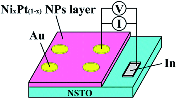 | ||
| Fig. 1 Schematic diagram of Au/NixPt(1−x) NPs/NSTO device. | ||
Results and discussion
Fig. 2a exhibits the EDS spectrum of the as-synthesized material, which are prepared by different composition ratios of Ni:Pt in the source reaction mixtures. The atomic ratio of the synthesized product is obtained by EDS, including 70:30, 80:20 and 100:0. The powder XRD spectra of the as-prepared NPs are shown in Fig. 2b and c. In Fig. 2b, four peaks of two proportional alloys about in the position of 29, 42, 49 and 72° are recognized as (111), (200), (220) and (311) planes, respectively. It is reasonable to conclude that (1) the peak position of the NixPt(1−x) alloy between the pure phase Pt and pure phase Ni and not are observed isolated Pt and Ni peaks, showing good crystal properties. (2) The peak position of the NixPt(1−x) alloy had a certain offset compared with Pt peak, and the degree of migration increasing with the increase of Ni content, indicating a increase in the lattice constant caused by replacing the Pt atoms with Ni atoms. The pure Ni NPs are shown in Fig. 2c by contrast. Four peaks of 44.44, 51.76, 76.26 and 92.94° are corresponded with (111), (200), (220) and (311) planes, respectively. All of these NixPt(1−x) NPs have a typical pattern of face-centered cubic (FCC) structure, in agreement with the TEM result (Fig. 3).
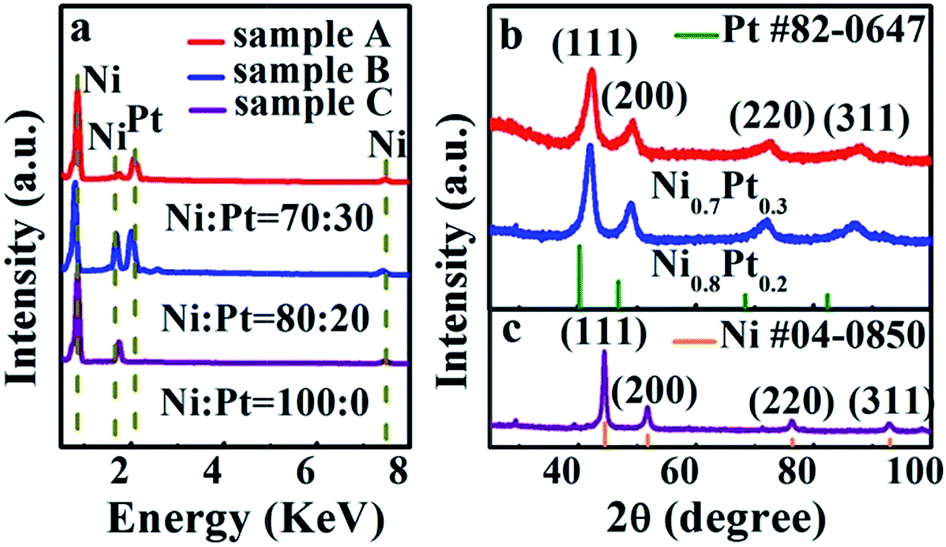 | ||
| Fig. 2 (a) EDS analysis reveals the atomic ratio of Ni and Pt. (b) XRD pattern of NixPt(1−x). (c) XRD pattern of Ni. | ||
 | ||
| Fig. 3 TEM image of the NixPt(1−x) NPs: (a) the size of Ni0.7Pt0.3 is about 20–30 nm. (b) The size of Ni0.8Pt0.2 is about 30–35 nm. (c) The size of Ni is about 45–50 nm. Typical HRTEM image: (d) single crystal Ni0.7Pt0.3 NPs. (e) Single crystal Ni0.8Pt0.2 NPs. (f) Single crystal Ni NPs. Inset of (a) is corresponding SAED pattern of Ni0.7Pt0.3. Inset of (b) is corresponding SAED pattern of Ni0.8Pt0.2. Inset of (c) is corresponding SAED pattern of Ni. | ||
The morphology and size of NixPt(1−x) NPs are observed by TEM at the same magnifications (Fig. 3a–c). Most of the as-prepared NixPt(1−x) NPs are in irregular, close to spherical shape. The particle size distributions are about 20–30 nm for Ni0.7Pt0.3 in Fig. 3a, 30–35 nm Ni0.8Pt0.2 in Fig. 3b, and 45–50 nm for Ni in Fig. 3c. The grain size seems to increase with the increasing Ni content. This is because in the reaction with more Ni, relatively higher monomer concentration will continue to grow after the nucleation. All of NixPt(1−x) NPs have apparently single crystal structures according to the HRTEM results in Fig. 3d–f. The lattice fringes with a d-spacing of 0.22 nm, 0.23 nm is consistent with the (111) planar distance of FCC crystalline Pt, 0.19 nm is consistent with the (200) planar distance of FCC crystalline Pt and the lattice fringes with a d-spacing of 0.20 nm consistent with the (111) planar distance of FCC crystalline Ni. To further confirm the crystallization, inset of Fig. 3a–c show selected area electron diffraction (SAED) patterns. The apparent concentric rings should be correspond to the (111), (200) and (220) planes with the consistent in d-spacing respectively, in agreement with XRD results shown in Fig. 2b and c. And we calculated that lattice parameter is a1 = 0.37 ± 0.01 nm (inset of Fig. 3a), a2 = 0.36 ± 0.01 nm (inset of Fig. 3b), which lies between standard FCC of Ni (0.352 nm) and Pt (0.392 nm). The percentage of Ni atomic from the lattice parameter was estimated about 70 ± 3%.
XPS measurements and analyses are conducted. Fig. 4a–c show the XPS curves for the NPs of Ni0.7Pt0.3, Ni0.8Pt0.2 and Ni, respectively. The fitting analyses reveal the peaks of Ni 2p3/2 for metallic nickel, Ni2+ from NiO, and their accompanying satellite peaks.32–34 The results of fitting analyses are listed in Table 2. It is noted that the oxidation peak of NixPt(1−x) NPs are significantly higher than that of pure Ni. This indicates that the surface Ni of the alloys is easier to be oxidized to Ni2+, than the pure Ni is.
 | ||
| Fig. 4 XPS fitting analysis of the peak of Ni 2p3/2 NixPt(1−x) NPs deposited on the substrates. (a) Ni0.7Pt0.3. (b) Ni0.8Pt0.2. (c) Ni. | ||
| Substance | Peak | Ni0.7Pt0.3 (eV) | Ni0.8Pt0.2 (eV) | Ni (eV) |
|---|---|---|---|---|
| Ni metal | Main | 852.78 | 852.65 | 852.57 |
| Sat. | 854.1 | 854.05 | 854.08 | |
| NiO | Main | 856.07 | 855.77 | 855.75 |
| Sat. | 861.28 | 861.43 | 861.27 |
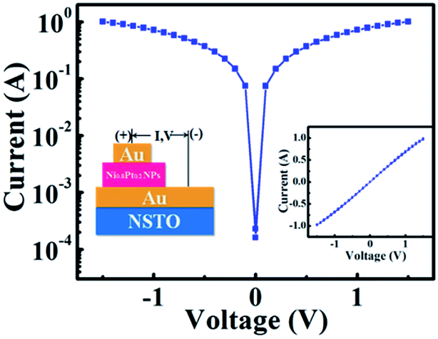
Fig. 5 partly demonstrates the asymmetrical I–V curves of the Au/NixPt(1−x) NPs/NSTO/In devices with different content of Ni. The remaining compositions of the devices are shown in Fig. S1.† The applied bias voltage is sweeping cyclically as 4 → 0 → −4 → 0 → 4 V. In the negative voltage phase, the current is in the negative direction accordingly. And in Fig. 5, the data in the negatively biased voltage are presented by multiplying a minus sign. In the procedure of sweeping, positive bias switches the device into the LRS. Then, a subsequent reverse sweep made LRS switched to the HRS, showing obvious bipolar RS effect. Even though the applied bias disappears, the LRS or HRS still persists, exhibiting a memory property. There is a small Ron/Roff ratio (about 3.4) at −2.4 V for Au/Ni NPs/NSTO. The ON/OFF ratio becomes even more pronounced with Au/NixPt(1−x) NPs/NSTO. Specifically, the Ron/Roff ratio is about 7.2 for Au/Ni0.7Pt0.3 NPs/NSTO and 8.6 for Au/Ni0.8Pt0.2 NPs/NSTO, at the same bias voltage of −2.4 V. The enhancement of the ON/OFF ratio with the latter two devices might likely due to (1) the smaller size of NixPt(1−x) NPs which introduces more structure defects, leading to local enhancement of the leakage current, (2) electron transferring occurs with the formation of NixPt(1−x) alloy. By the alloying the electron distribution shifts away from Ni, making it more similar to a cation. The cation-like Ni in the surface is apt to react with oxygen, forming NiOx. This is consistent with the XPS results in that the oxidation peaks of the NixPt(1−x) NPs are significantly higher than that of pure Ni in XPS analysis, discussed former in Fig. 4. Inset of Fig. 5 describes the Au/Ni0.8Pt0.2NPs/NSTO/In device 50 times of continuous circular sweep, showing cycling endurance of the RS characteristics.
 | ||
| Fig. 5 I–V characteristics of the Au/NixPt(1−x) NPs/NSTO/In devices plotted in semilog scale. The inset is for the I–V characteristics of the Au/Ni0.8Pt0.2 NPs/NSTO/In device, taken by 50 times of continuous voltage sweeping measurements showing good stability. | ||
The I–V curve of the Au/Ni0.8Pt0.2/Au/NSTO device has been taken, shown in Fig. 6. The applied sweeping bias voltage is set in the cyclic order 1.5 → 0 → −1.5 → 0 → 1.5 V. The I–V data are plotted in semilog scale, and also in the linear scale in the inset. It reveals obviously that the Au/NixPt(1−x) NPs junction is an ohmic contact, as well as the In/NSTO contact. In addition, there is no hysteresis observed. It demonstrates that the RS effects is irrelevant to the Au/NixPt(1−x) NPs interfaces.
 | ||
| Fig. 6 I–V characteristics of the Au/Ni0.8Pt0.2 NPs/Au/NSTO device plotted in semilog scale. A simple sketch for the device structure is provided, the inset is for the I–V curve in linear scale. | ||
The effects of annealing in the atmospheres of different gases on the I–V properties are investigated for the devices with Ni0.8Pt0.2 and Ni NPs. The annealing is taken places in the atmospheres of oxygen and argon–hydrogen mixture (5% hydrogen, 95% argon) at 500 °C for 30 min. The I–V curves in semilog scale are shown in Fig. 7a and b for the argon–hydrogen and oxygen treatments, respectively. The magnitude of irreversibility with both cases of the I–V hysteresis is suppressed perceivably in comparison with the data without annealing shown in Fig. 5. This suggests that defects play an important role in the irreversible transport behavior. Another feature is further noted. In comparison to the data shown in Fig. 5, the resistance for Au/NixPt(1−x)/NSTO is smaller in Fig. 7a (annealed in argon–hydrogen), while larger in Fig. 7b (annealed in oxygen). When adding a positive bias on the Au electrode, electrons are released from the interface and the net plus charge produced lower the barrier height of the interface, which makes LRS. However, when adding a negative bias, the interface layer accumulates a large amount of electrons and produced higher barrier height of the interface, the device changed in the HRS.8,35,36 Through controlling the annealing atmosphere, the concentration of NixPt(1−x) NPs/NSTO oxygen vacancies can be tuned. Annealing in an oxidizing atmosphere, oxygen gradually diffuses into the NixPt(1−x) NPs/NSTO depletion layer. The number of oxygen vacancies decreases with the increase of oxygen content in the depletion layer. On the other hand, annealing in the reducing atmosphere increases the concentration of NixPt(1−x)/NSTO oxygen vacancies.37 Therefore, annealing in an O2 atmosphere will reduce the concentration of NixPt(1−x)/NSTO oxygen vacancies so that the RS almost disappeared, but we can still see that the RS of the NixPt(1−x) alloy is more obvious than that of the pure Ni; annealing in an argon–hydrogen atmosphere will increase the concentration of NixPt(1−x)/NSTO oxygen vacancies so that the RS may increases.38 However, due to the crystalline quality of the NixPt(1−x)/NSTO becomes better and the defect decreases, the RS is reduced.
 | ||
| Fig. 7 The I–V characteristics of Au/NixPt(1−x) NPs/NSTO/In devices annealed in different atmosphere. The I–V curves for devices with Ni treated in the same conditions are also plotted as a reference. The bias voltage swept is 4 → 0 → −4 → 0 → 4 V. (a) Annealed in Ar + H2, (b) annealed in O2. | ||
In order to get a better explanation about the RS in different proportions Au/NixPt(1−x)/NSTO memory devices, I–V curves in Fig. 5 are repaint in a log–log scale. Fig. 8 clearly exhibits the different linear fitting results for the negative bias region using as-synthesized products at 300 K in bipolar memory switching for one switching cycle. It can be divided into three parts: two linear regions for smaller bias voltages and a nonlinear increase region for the between two smaller bias voltages. At low bias region, the curves have a linear region with a slope of ∼1.0 from 0–0.9 V for Fig. 8a, 0–1.5 V for Fig. 8c, indicating an ohmic conduction due to the radio of log(I)/log(V) close to 1.0. This is because the thermally induced free carrier density dominants the conduction; the density of injected charge carriers is lower than that of thermally generated free carriers.39 However, the slope of the corresponding curve for Ni0.8Pt0.2 is 2.0, which could be easily classified in terms of the SCLC mechanism. It is followed by a large slope in region on the steep region characterized by: 1.0–3.9 V for Fig. 8a, 2.1–3.8 V for Fig. 8b and 2.2–4.0 V for Fig. 8c. In this bulk limited mechanism, the transport is corresponded to Child's law.40
 | (1) |
 | (2) |
 | ||
| Fig. 8 The linear fitting of I–V characteristic of Au/NixPt(1−x) NPs/NSTO at negative voltages: (a) Au/Ni0.7Pt0.3 NPs/NSTO, slope1 = 2.3, slope2 = 1.1, slope3 = 3.6, slope4 = 1.2. (b) Au/Ni0.8Pt0.2 NPs/NSTO, slope1 = 2.2, slope2 = 4.7, slope3 = 2.0. (c) Au/Ni NPs/NSTO, slope1 = 1.4, slope2 = 2.4, slope3 = 0.9. | ||
The overall RS mechanism of the NixPt(1−x)/NSTO interfaces can be understood by considering the trapping/detrapping of charge carriers and the modulation of the depletion layer at the interface. Because the carrier concentration of NixPt(1−x) is much higher than that of NSTO, the depletion layer is mainly at the NixPt(1−x) side. Furthermore, positively charged oxygen vacancies and their complexes can serve as traps for charged carriers at the NixPt(1−x)/NSTO interface. In the positive parts of the I–V characteristics, lots of electrons flowing from the NixPt(1−x)/NSTO interface get trapped, giving rise to a high leakage current at the high forward bias (LRS). Consequently, as the voltage sweeps to the negative side, the polarity of both voltage and current is reversed. When the Au electrode is negative biased, the positive charged oxygen vacancies are removed from the interface region; as a consequence, the defect density and the leakage current at the interface are reduced, and the device is reset to the HRS. In the transition from HRS to LRS, the steep current increase is a result of rapidly filled traps. The sweep of positive voltage moves the oxygen vacancies into the interface region, which leads to trapping-dominated transport and sets the device to LRS.40 Our experiments suggest that the NixPt(1−x)/NSTO heterostructure behaves as a switchable diode, which may present more functionalities in future studies. Furthermore, both the electronic SCL conduction and the ionic vacancy migration are indispensable ingredients in the data interpretation, producing complementary effects.
Conclusions
In summary, we have prepared NixPt(1−x) NPs and fabricated Au/NixPt(1−x) NPs/NSTO devices. The RS effects of the devices are compared with different Ni components in 300 K. The ON/OFF ratio of Au/NixPt(1−x) NPs/NSTO increases with the increasing the content of Ni, and the RS effect of the NixPt(1−x) NPs is more obvious than that of the pure Ni. We cycled the Au/Ni0.8Pt0.2 NPs/NSTO device 50 times, impling good endurance performance. By further fitting the I–V curves, we prove that conduction mechanism is dominated by SCLC and TFL. Then we annealed the devices at 500 °C in different atmosphere, which make RS effect becoming smaller. Annealing in the atmosphere of oxygen triggers RS becomes smaller due to the depletion of oxygen vacancies in the layer. Whereas annealing in the atmosphere of argon–hydrogen made the RS becomes smaller, probably due to the improvement of crystalline quality and the decreasing of the defects at the NixPt(1−x)/NSTO interfaces.Acknowledgements
This work was supported by the National Natural Science Foundation of China (No. 51371015, 51331002 and 51571006), the Beijing Natural Science Foundation (No. 2142018) and the Fundamental Research Funds for the Central Universities (FRF-BR-15-009B).Notes and references
- I. Hwang, M. J. Lee, G. H. Buh, J. Bae, J. Choi, J. S. Kim, S. Hong, Y. S. Kim, I. S. Byun and S. W. Lee, Appl. Phys. Lett., 2010, 97, 052106 CrossRef
.
- S. Zhong, S. Duan and Y. Cui, RSC Adv., 2014, 4, 40924–40929 RSC
- X. B. Yan, Y. D. Xia, H. N. Xu, X. Gao, H. T. Li, R. Li, J. Yin and Z. G. Liu, Appl. Phys. Lett., 2010, 97, 112101 CrossRef
- S. Chandrakishore and A. Pandurangan, RSC Adv., 2013, 4, 9905–9911 RSC
- J. R. Jameson, Y. Fukuzumi, Z. Wang, P. Griffin, K. Tsunoda, G. I. Meijer and Y. Nishi, Appl. Phys. Lett., 2007, 91, 112101 CrossRef
- M. H. Lee, K. M. Kim, G. H. Kim, J. Y. Seok, S. J. Song, J. Ho Yoon and C. Seong Hwang, Appl. Phys. Lett., 2010, 96, 152909 CrossRef
- I. G. Baek, M. S. Lee, S. Seo, M. J. Lee, D. H. Seo, D. S. Suh, J. C. Park, S. O. Park, H. S. Kim, I. K. Yoo, U. I. Chung and J. T. Moon, IEEE International Electron Devices Meeting 2004, Technical Digest, 2004, p. 587 Search PubMed
- Y. Cui, S. Yin, D. Wang, G. Xing, S. Leng and R. Wang, J. Appl. Phys., 2010, 108, 104506 CrossRef
- A. Sawa, Mater. Today, 2008, 11, 28–36 CrossRef CAS
- I. G. Baek, C. J. Park, H. Ju, D. J. Seong, H. S. Ahn, J. H. Kim, M. K. Yang, S. H. Song, E. M. Kim, S. O. Park, C. H. Park, C. W. Song, G. T. Jeong, S. Choi, H. K. Kang, C. Chung and Ieee, 2011 Ieee International Electron Devices Meeting (Iedm), 2011 Search PubMed
- A. Beck, J. G. Bednorz, C. Gerber, C. Rossel and D. Widmer, Appl. Phys. Lett., 2000, 77, 139–141 CrossRef CAS
- Y. Cui and R. Wang, Appl. Phys. Lett., 2007, 91, 233513 CrossRef
- D. C. Kim, S. Seo, S. E. Ahn, D. S. Suh, M. J. Lee, B. H. Park, I. K. Yoo, I. G. Baek, H. J. Kim, E. K. Yim, J. E. Lee, S. O. Park, H. S. Kim, U. I. Chung, J. T. Moon and B. I. Ryu, Appl. Phys. Lett., 2006, 88, 202102 CrossRef
- Y. D. Xia, W. Y. He, L. Chen, X. K. Meng and Z. G. Liu, Appl. Phys. Lett., 2007, 90, 022907 CrossRef
- H. Sim, H. Choi, D. Lee, M. Chang, D. Choi, Y. Son, E. H. Lee, W. Kim, Y. Park, I. K. Yoo, H. Hwang and Ieee, Excellent resistance switching characteristics of Pt/SrTiO (3) Schottky junction for multi-bit nonvolatile memory application, 2005 Search PubMed
- D. S. Kim, Y. H. Kim, C. E. Lee and Y. T. Kim, Phys. Rev. B: Condens. Matter Mater. Phys., 2006, 74, 174430 CrossRef
- Q. Sun, Z. Ren, R. M. Wang, N. Wang and X. Cao, J. Mater. Chem., 2011, 21, 1925–1930 RSC
- P. Li, W. Chen, W. Liu, Z. A. Li, Y. Cui, A. Huang, R. Wang and C. Chen, J. Phys. Chem. C, 2010, 114, 7721–7726 CAS
- Q. Sun, W. Liu and R. M. Wang, CrystEngComm, 2012, 14, 5151–5154 RSC
- H. Lang, S. Maldonado, K. J. Stevenson and B. D. Chandler, J. Am. Chem. Soc., 2004, 126, 12949–12956 CrossRef CAS PubMed
- J. W. Hong, S. W. Kang, B. S. Choi, D. Kim, S. B. Lee and S. W. Han, ACS Nano, 2012, 6, 2410–2419 CrossRef CAS PubMed
- C. Koenigsmann, W. P. Zhou, R. R. Adzic, E. Sutter and S. S. Wong, Nano Lett., 2010, 10, 2806–2811 CrossRef CAS PubMed
- C. Wang, H. Daimon, T. Onodera, T. Koda and S. H. Sun, Angew. Chem., Int. Ed., 2008, 47, 3588–3591 CrossRef CAS PubMed
- J. X. Wang, C. Ma, Y. M. Choi, D. Su, Y. M. Zhu, P. Liu, R. Si, M. B. Vukmirovic, Y. Zhang and R. R. Adzic, J. Am. Chem. Soc., 2011, 133, 13551–13557 CrossRef CAS PubMed
- H. Ataee-Esfahani, Y. Nemoto, L. Wang and Y. Yamauchi, Chem. Commun., 2011, 47, 3885–3887 RSC
- A. X. Shan, M. Cheng, H. S. Fan, Z. C. Chen, R. M. Wang and C. P. Chen, Prog. Nat. Sci.: Mater. Int., 2014, 24, 175–178 CrossRef CAS
- T. Y. Xia, J. L. Liu, S. G. Wang, C. Wang, Y. Sun, L. Gu and R. M. Wang, ACS Appl. Mater. Interfaces, 2016, 8, 10841–10849 CAS
- Y. Cui, Y. Tian, W. Liu, Y. Li, R. Wang and T. Wu, AIP Adv., 2011, 1, 042129 CrossRef
- Y. Cui, W. Liu and R. Wang, Phys. Chem. Chem. Phys., 2013, 15, 6804–6808 RSC
- W. H. Guan, S. B. Long, Q. Liu, M. Liu and W. Wang, IEEE Electron Device Lett., 2008, 29, 434–437 CrossRef CAS
- P. Mondal, A. Sinha, N. Salam, A. S. Roy, N. R. Jana and S. M. Islam, RSC Adv., 2013, 3, 5615–5623 RSC
- H. W. Nesbitt, D. Legrand and G. M. Bancroft, Phys. Chem. Miner., 2000, 27, 357–366 CrossRef CAS
- A. X. Shan, Z. C. Chen, B. Q. Li, C. P. Chen and R. M. Wang, J. Mater. Chem. A, 2015, 3, 1031–1036 CAS
- J. L. Rodriguez, M. A. Valenzuela, T. Poznyak, L. Lartundo and I. Chairez, J. Hazard. Mater., 2013, 262, 472–481 CrossRef CAS PubMed
- D. J. Seong, M. Jo, D. Lee and H. Hwangz, Electrochem. Solid-State Lett., 2007, 10, H168–H170 CrossRef CAS
- K. Park and J. S. Lee, RSC Adv., 2016, 6, 21736–21741 RSC
- N. S. Kamarozaman, M. F. Mohamed Soder, M. Z. Musa, R. A. Bakar, W. F. H. Abdullah, S. H. Herman and M. Rusop Mahmood, Adv. Mater. Res., 2014, 925, 125–129 CrossRef
- W. G. Kim and S. W. Rhee, Microelectron. Eng., 2009, 86, 2153–2156 CrossRef CAS
- S. Y. Wang, B. L. Cheng, C. Wang, S. Y. Dai, H. B. Lu, Y. L. Zhou, Z. H. Chen and G. Z. Yang, Appl. Phys. Lett., 2004, 84, 4116–4118 CrossRef CAS
- Y. Cui, H. Peng, S. Wu, R. Wang and T. Wu, ACS Appl. Mater. Interfaces, 2013, 5, 1213–1217 CAS
- Z. Wang, F. Zeng, J. Yang, C. Chen and F. Pan, ACS Appl. Mater. Interfaces, 2012, 4, 447–453 CAS
- Y. C. Yang, F. Pan, Q. Liu, M. Liu and F. Zeng, Nano Lett., 2009, 9, 1636–1643 CrossRef CAS PubMed
- H. Yang, Y. Q. Wang, H. Wang and Q. X. Jia, Appl. Phys. Lett., 2010, 96, 012909 CrossRef
- M. A. Lampert, Phys. Rev., 1956, 103, 1648–1656 CrossRef CAS
Footnote |
| † Electronic supplementary information (ESI) available: Fig. S1 I–V characteristics of Au/NixPt(1−x) NPs/NSTO/In devices. See DOI: 10.1039/c6ra24987f |
| This journal is © The Royal Society of Chemistry 2017 |