
 Open Access Article
 This Open Access Article is licensed under a Creative Commons Attribution-Non Commercial 3.0 Unported Licence
Fabrication of PDMS microfluidic devices with 3D wax jetting†
Zong'an Li*ab,
Jiquan Yangb,
Kelou Lib,
Li Zhuc and
Wencheng Tanga
aSoutheast University, Nanjing, Jiangsu, China. E-mail: 101000185@seu.edu.cn; zonganli@seu.edu.cn; Tel: +86-136-751-07447
bNanjing Normal University, Jiangsu Key Laboratory of 3D Printing Equipment and Manufacturing, Nanjing, Jiangsu, China. E-mail: 63047@njnu.edu.cn; 151802016@stu.njnu.edu.cn
cNanjing University of Science and Technology, Nanjing, Jiangsu, China. E-mail: zhuli@njust.edu.cn
First published on 13th January 2017
Abstract
In this paper, a method for making 3D polydimethylsiloxane (PDMS)microfluidic chips with a modified open-source 3D wax printer is demonstrated. The wax was generated with a glass nozzle and a lead zirconate titanate (PZT) actuator. The influence of 3D printing parameters including the degree of overlap and the filling distance between the filling paths on the wax mold were studied. Some typical 3D wax molds such as a 3D shell structure, a 3D letter “U” and a 3D bridge were prepared. Also fabricated were key, functional 3D microfluidic devices including a basket-weave network, a 3D chaotic passive mixer, and a microdroplet generator. True 3D network microflowing was accomplished. This method offers a simple, low-cost way to make 3D microfluidic chips in a short time without clean-room facilities.
Introduction
Microfluidic chips have become a very important element in the micro-total-analysis system (μ-TAS) since the chip was first used for chemical analysis in 1990.1 Microfluidic chips can improve efficiency because of their micro- or nanoscale flow and large-scale integration, and make the analysis process integratable, automatable, and portable. In the past 2 decades, microfluidic chips have been widely applied for such purposes as micromixing and separating,2,3 biological and chemical analysis,4–6 and microemulsifying and encapsulating.7,8Based on the connectivity of their channels, microfluidic chips can be roughly divided into 3 categories: 2 dimensional (planar), quasi 3D (stacked 2D planes) and real 3D networked micro channels.9 The latter category consists of bridge features, where the channels can cross each other without connecting, and this enables these chips to perform complex processes like basket-weave flowing.
Currently techniques for large-scale replication and production of planar and 3D microfluidic devices include micro-machining,10 embossing,11,12 in situ construction injection molding,13 laser ablation,14,15 and soft lithography.16,17 Some of those techniques require expensive equipment and are labor intensive. For the analysis in the laboratory environment, small-scale production is preferred. Therefore, PDMS casting-based 3D molding (soft lithography) is convenient and simply the easiest way to rapidly prototype of planar and 3D microfluidic devices. Many simplified microfabrication methods have been used for creating 2D or 3D master molds, including UV exposure on photosensitive polymers,18 Shrinky-Dink,19 etching,20 ice water patterning,21 liquid molding,22 micromachining,23 3D printing24,25 and so on. The mold preparation methods mentioned above except 3D printing are 2D or quasi 2D, and thus not suited for the real 3D work. The 3D printing and its combination with soft lithography offers a high resolution and rapid way to help simplify the fabrication process for 3D microfluidic devices.
The 3D printing methods used for the direct and replicating fabrication of microfluidic devices include fused deposition modeling (FDM),26–28 stereolithography (SLA)29–31 and UV curing of microdispensed droplets.32,33 Directly 3D printing of 3D microfluidic chips offers great topography flexibility, because during the 3D printing process multiple 2D layers are stacked to construct a true 3D channel network. The limitation of 3D printing directly the microfluidic devices lies mainly in the material used. Materials such as acrylonitrile butadiene styrene (ABS) or polylactic acid (PLA) for the FDM 3D printing and the photosensitive resin for the SLA 3D printing draw back in the light transmitting compared with PDMS. The replication of non-sacrificial 3D printed mold requires the PDMS heal by itself on the broken location to form network channels when peeled off from the molds, thus it is still not suitable for complicated true 3D molds.
3D printing of sacrificial mold34–38 is rapid and cost efficient, can avoid solid-to-solid bonding, and is possible to directly print the PDMS micro channels in a single process, enabling rapid prototyping of complex structures. Thus it becomes a trend for the 3D PDMS microfluidics. Most of the 3D printed sacrificial molds mentioned in the literatures are based on the extruding principle like FDM. The EGaIn metal,34 sugar (isomalt or maltitol),35,36 carbohydrate glass37 and ABS38 were extruded out of the nozzle and formed into filament for the additive manufacturing. The extruding methods used maltitol, EGaIn and carbohydrate glass require another PDMS extruding nozzle to add the support PDMS when printing. The channels on different layers need pillars as connectors to form 3D channels. The minimum diameter of the filament diameter is 0.5 mm for the ABS printing and the resulted 3D channel is up to 2 mm. The true 3D micro channels such as the basket weave structure is difficult to be prepared with these methods. The low-cost, easy, and high resolution fabrication method for the 3D sacrificial mold is necessary.
Compared with the extruding, micro jetting based 3D printing has advantages that high resolution, non contract, and easy to prepared pillars. Wax material is inexpensive, freely available, and easily sacrificed at 80 °C, making it acceptable for use with PDMS. Because of these characteristics, wax has been used for planar microfluidic chips.39,40 What's more, the wax can be jetted after melted into liquid. The development of 3D wax molds with micro jetting based 3D printing technology is promising.
This paper introduces a novel may of making 3D sacrificial wax mold with a modified open-source FDM 3D printer. In our study, wax was jetted with a PZT actuator and a glass nozzle. A relay controlled by the enable signal of the extruding step motor was used to control the start-stop jetting of wax droplets. Firstly, we studied 3D printing parameters such as the degree of overlap and distance between the filling paths on the wax mold. Then, we printed some typical 3D wax molds including a 3D shell, a 3D letter “U” and a 3D bridge with the modified wax printer, and studied the relationship between the forming capability and the sliced layer thickness. Some key functional microfluidic chips including a micromixer, a micro water in oil (W/O) droplet generator, and a basket-weave network were prepared, and the demonstration experiments were carried out on the 3D microfluidic chips.
Material
Glass tubing 1.0 mm × 0.6 mm was from Nanjing Lupu Chemical Co., Ltd. Paraffin wax 56/58 was supplied by Shanghai Specimen and Model Factory. Erioglaucine disodium salt (BR, 85%, CAS no. 3844-45-9) and tartrazine BS (85% CAS no. 1934-21-0) were purchased from Shanghai Jinsui Bio-tec Co., Ltd. AR graded ethanol was from Nanjing Chemical Reagent Co., Ltd. Sylgard 184, silicon elastomer was supplied by Dow Corning Corp. Corn oil was from Xiwang Food Co., Ltd.Method
Generation of wax droplets
An open-source FDM 3D printer was modified for the 3D movements and the start-stop jetting signal. The extruder part of the original FDM printer except the heating rod and the thermocouple probe, was removed, and replaced with a PZT based wax droplet generator. The Marlin RepRap firmware was modified. The definition of EXTRUDE_MINTEMP in the h-type file of “configuration” was set at 15 to make the extruder heating rod work at 75 °C. The start-stop signal was a voltage signal of 5 V drawn from the enable signal of the extruder stepper motor input signals. The start-stop signal was actuated by a relay switch connected to the input signal of the PZT actuator. The wax droplet generator comprised a piezoelectric actuator (PI P-844.10), a glass nozzle, a wax container, and a connector, as shown in Fig. 1. A similar system was used in our previous work for the fabrication of planar paper microfluidic devices.41 A schematic of the modified 3D wax printer is shown in Fig. 1, which also shows an enlargement of the glass nozzle. The picture of the system is shown in the Fig. S1,† and the picture of the glass nozzle is shown in the Fig. S2.†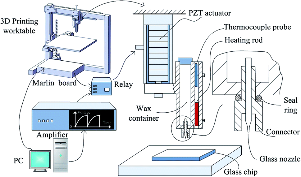 | ||
| Fig. 1 Schematic of the 3D wax printing system. | ||
3D printing of wax mold
3D stereolithography (STL) data models used to produce network microfluidic chips were created with CAD software and imported into the slicing software. The STL data were transferred to G-code, a numerical control programming language; the paths of a representative G-code-generated slice are shown in Fig. 2b. The relative coordinate system code G91 was used to raise the nozzle when finishing one piece of a path. To stop the jetting, code M84 E0 was used to draw down the enable signal on the extruder stepper motor. The specific G-codes are further explained in the supplementary material. | ||
| Fig. 2 (a) Computer STL model of a 3D network, (b–g) paths of the G-code generated slice. | ||
Replicating and bonding of PDMS microfluidic chips
FDM 3D printed PLA rings was placed on a quartz glass chip with a printed wax mold and adhered with ethylene vinyl acetate copolymer hot melt adhesive to prevent leaking. Liquid silicon elastomers A and B liquid with a volume ratio of 10![[thin space (1/6-em)]](https://www.rsc.org/images/entities/char_2009.gif) :1 were thoroughly mixed by a magnetic stirrer at 120 revolutions per minute and then degassed in a vacuum drying oven. The PDMS liquid was slowly poured on the wax mold and then the glass chip was laid in the drying oven at 40 °C for 24 hours to cure the PDMS. The cured PDMS chips was then cut along the ring boundary and peeled off the glass chip. The PDMS chip was soaked in cyclohexane solution for 10 minutes, washed in deionized water, and then dried by nitrogen gas. After that, the PDMS chip was soaked in 80 °C deionized water for 10 minutes. The chip was then took out quickly, washed in ethanol AR, cleaned by the nitrogen gas and dried in the 85 °C oven for 20 minutes. Then the edge of the chip was cut carefully to remove the burrs, drilled, and cleaned. Finally the chip was plasma treated and bonded with a well-cleaned glass chip. The total time for a microfluidic device from designing to producing required two work days.
:1 were thoroughly mixed by a magnetic stirrer at 120 revolutions per minute and then degassed in a vacuum drying oven. The PDMS liquid was slowly poured on the wax mold and then the glass chip was laid in the drying oven at 40 °C for 24 hours to cure the PDMS. The cured PDMS chips was then cut along the ring boundary and peeled off the glass chip. The PDMS chip was soaked in cyclohexane solution for 10 minutes, washed in deionized water, and then dried by nitrogen gas. After that, the PDMS chip was soaked in 80 °C deionized water for 10 minutes. The chip was then took out quickly, washed in ethanol AR, cleaned by the nitrogen gas and dried in the 85 °C oven for 20 minutes. Then the edge of the chip was cut carefully to remove the burrs, drilled, and cleaned. Finally the chip was plasma treated and bonded with a well-cleaned glass chip. The total time for a microfluidic device from designing to producing required two work days.
Demonstration of PDMS microfluidic chips
Micro-mixing, micro W/O droplet generation and network flowing were demonstrated on the PDMS microfluidic chips. A 4 channel syringe pump (LSP04-1A, Longer Precision Pump Co., Ltd) was used to feed the fluid. Blue and yellow dyes, 800 μM erioglaucine (blue dye) and 1870 μM tartrazine (yellow dye) respectively, were prepared and injected into the inlet channels of a passive micromixer separately in a speed of 2, 8, 10, and 100 μL min−1. For the micro W/O droplet generating, corn oil and the blue dye were pumped into the inlet channels separately at a rate of 2 and 10 μL min−1. For network flowing, the blue dye and yellow dyes were separately injected into the inlet channels of the network microfluidic chip at 100 μL min−1.Result and discussion
Influence of 3D printing parameters on the wax mold
We studied the influence of jetting parameters of the PZT driving signal such as the voltage and frequency, the influence of nozzle diameter on the size of wax droplets, and the degree of overlap of the wax line structure. Results showed that the size of the wax droplets ranged from 150 μm to 375 μm. The array of 35 wax droplets with 45 V voltage was prepared and measured by the outline circle diameter. The coefficient of variation (CV) of the diameter of the jetted wax droplets was under 4.0% and this showed a well uniformity. The surface of the wax line structure was influenced by the degree of overlap k as shown in Fig. 3. k is defined as
 | (1) |
 | ||
| Fig. 3 Wax line structures jetted with these parameters: degree of overlap 0 to 80%, voltage 40 V, frequency 11 Hz, and nozzle diameter 75 μm, (a) schematic of the droplet overlap, (b) k = 0, (c) k = 10%, (d) k = 30%, (e) k = 50%, (f) k = 80%. | ||
The 3D wax mold model was composed of sliced layers. Each layer was constructed of profile paths and filling paths, and the option of filling or not depended on the distance of the profile. The filling pattern used in this study was a straight line, and the direction was rotated 90° between each sliced layer. For the 3D printing with filling option, the filling distance Df (Fig. 4) was defined as the distance between the neighboring filling lines.
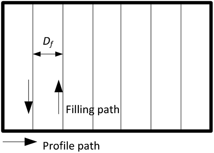 | ||
| Fig. 4 Schematic of the 3D printing paths. | ||
STL cuboids with 1.5 mm side were sliced filling distances Df specified at 100 μm, 80 μm, and 60 μm respectively. Then, the cuboids were printed on glass slides using a nozzle diameter of 75 μm, a voltage of 30 V, a frequency of 10 Hz and a speed of 90 mm per minute. Results are shown in the Fig. 5. The wax droplets on the profile paths were round and similar to those in the single wax line structure in Fig. 3. In the filling path, the wax droplet outline was polygonal, caused by the overlap of the left and back sides wax droplets. When Df was reduced to less than 30% of the wax droplet diameter (60 μm on 180 μm), as shown in Fig. 5g and h, the microscope could focus on only 8 pieces of filling paths at 5× magnification, and 4 pieces at 10×. The side view in Fig. 5i showed that the filling wax lines grew above of the glass slide; the angle between the glass slide surface and the wax structure surface was 23°. This indicates that real 3D structures with suspended parts can be prepared.
 | ||
| Fig. 5 Images of a single layer of 3D printed wax structures taken by an Olympus DP27 digital camera through an Olympus CKX41 inverted microscope, (a–c) printed wax slices with a filling distance of 100 μm and magnification of 5×, 10× and 40× respectively, (d–f) slices with a filling distance of 80 μm, magnification of 5×, 10× and 40× respectively, (g and h) slices with a filling distance of 60 μm, magnification of 5× and 10× respectively, (i) left side view of wax slice with a filling distance of 60 μm. | ||
3D printing of wax structures
Four kinds of 3D models were designed with CAD software and the 3D wax mold was printed on a cleaned quartz glass chip. Three distances in z direction were defined: the sliced layer thickness (Ds), the printed layer thickness (Dp) and the printing head rise distance between layers (Dz). The final height of the printed model (h) was calculated by h = Dp × n, where n is the number of layers. This formulation was theoretically derived, and actually the height of the first layer (Dp1) was a little larger than other layers. We determined printed layer thickness by the average of 10 printed layers. For the models without surface unevenness such as cylinders and cubes, the printing quality, except the final height, was not influenced by the number of layers. For the models with suspended structures, Ds was related to the suspended structures, and the printing requirement was that the horizontal extending distance between the neighboring sliced layers be less than 30% of the diameter size of the wax droplet.The first 3D model was a 3D shell. In the plane view the model was square, and in the elevation view from either side it was roughly a truncated pyramid, because the lengths of the sides decreased as the structure grew spirally from the bottom. The designed model was sliced to 90 layers without filling, and the layers were 50 μm thick. The printed wall thickness was approximately 300 μm, and the total height was 3 mm (Fig. 6a–c). Air movement caused by the room air conditioning or natural wind could displace the wax droplets, so the printing environment was sheltered.
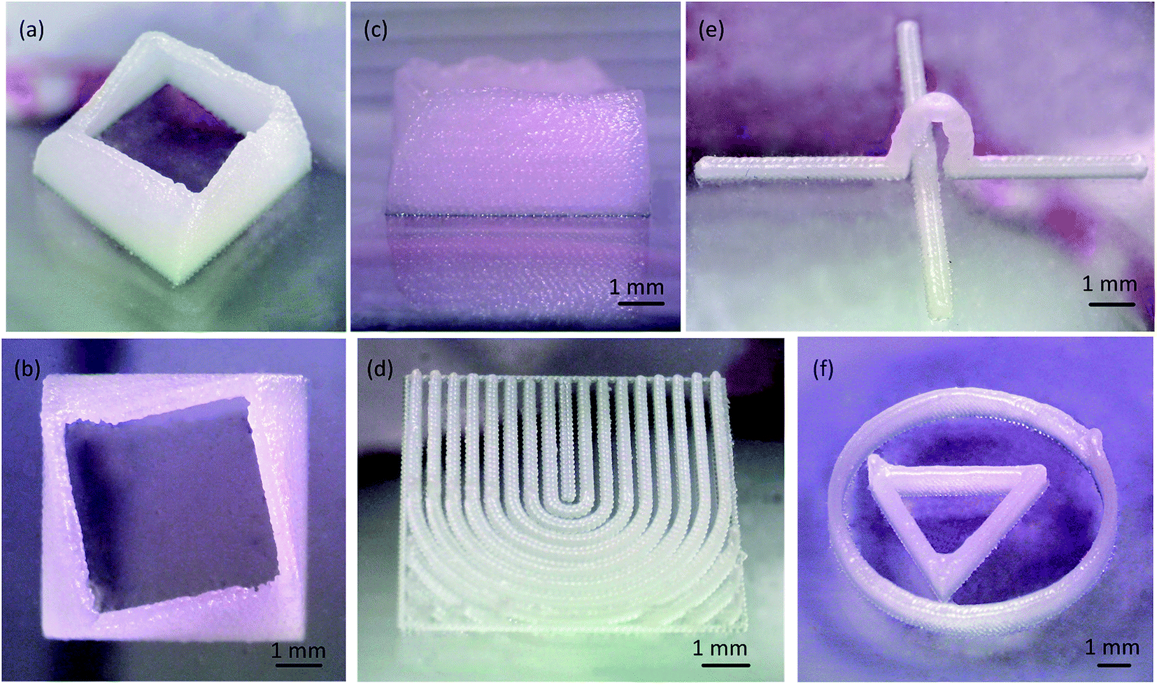 | ||
| Fig. 6 3D printed wax structures photographed through a handheld microscope, (a) isometric view of the spirally growing square shell, (b) plane view of the shell, (c) elevation view of the shell, (d) 3D letter U shape, (e) bridge model for real 3D fluid channels, (f) 3D printed triangular and circular structures. | ||
The second 3D model resembled a letter U without filling paths. The U was composed of wall structures, and the height of the walls symmetrically increased from the middle to the both sides. The printed result is shown in Fig. 6d. The printed wall thickness was 300 μm. There is a boundary trail on the walls, especially clear on the wax line right in the middle.
Also designed was a 3D model for real 3D microfluidic channels. The mold was a 15 mm straight line stepped over by an arc bridge (Fig. 6e). The printed height of the arc top was 3 mm, and the sliced layer thickness was 400 μm. The real difficulty was the closure of the bridge structure. The extending distance should be less than 30% of the diameter size of the wax droplets. The empty move speed was at 500 mm min−1, and printing move speed was at 90 mm min−1. The 3D shell structure required 18 minutes for printing. The arc bridge structure needed only 5 minutes.
Finally, we raised the jetting temperature to 105 °C, and printed a triangular structure surrounded by a circular structure (Fig. 6f). The surface was smoother than that fabricated at 75 °C because the flow property was improved. The wall thickness was 350 μm. At the ending and starting locations, there are small stacks of wax droplets. In the FDM printing, the extruder step motor draws back the thread to prevent residual plastic material from flowing out of the nozzle and raises the print quality. In the drop-on-demand printing, the current of the amplified signal controlled by the relay has an effect on the PZT actuator. To avoid these stacks of droplets, corresponding of the driving signal of the PZT actuator to the pulse signals of the stepper motor is needed. Another influence was the accelerating process of the 3D printing work table.
The surfaces of 3D printed objects by the traditional FDM method had a clear interface between the plastic, metal or sugar filaments in the same layer and between layers. SLA and UV curing method could produce 3D object very smooth surface, but the molds were not easy to be sacrificed. The wax structure surfaces produced by the modified wax 3D printer were covered with zig-zag structures in the same layer and between layers (Fig. S3†). We could observe the trail of the wax droplet stacking on the pillar surface in the bridge wax structure. The preparation of pillars required the accuracy of the dispensed droplet position and the 3D work table. The repeat positioning accuracy of the work table used for open-source FDM printing was ±10 μm, and the dispensed droplet position accuracy was influenced by the air movement and the move speed of the glass nozzle (Fig. S4†). We required the printing environment sheltered and the printing speed was under 90 mm min−1. This accuracy is sufficient for the micro structures large than 100 μm, but for the nano-scale micro-fabrication, a work table with positioning accuracy less than ±5 μm was needed.
The fabrication of bridge structures was influenced by the mold size, shape, and slicing parameters. One layer in the micro-pillar only needed several wax droplets, and this required the work table moved a very short distance. Thus, the designing size of the pillar was 200 μm. We tried triangular bridge of 30°, 45°, and 60°. The triangular bridge of 30° was totally failed because reducing the sliced layer thickness would increase the total bridge height actually printed (h = Dp × n) and with the sliced layer thickness more than 80 μm, some wax droplets dripped on the bottom. The triangular bridges with an angle more than 45° were easier to be prepared. Another difficulty for the bridge structure is the folding of the bridge top, and it required smooth transition from one side to the other.
3D printed microfluidic chips for passive micromixing
Sufficient mixing is one very important requirement for microfluidic chips to realize the microfluidic functions. The Reynolds number a micro-scale flowing is usually very low, so most of the fluid is in a laminar flowing (i.e., hydrodynamically stable) area. This makes most fluid mixing occur by diffusion, which can be very slow. Research results show that the barriers in the flow channel could change the form of the streamline, thus increasing mixing efficiency.2,4 After the wax mold was replicated with PDMS, the micro zig-zag structures caused by wax droplet overlaps were replicated in the fluid channel. The zig-zag structures acted as barriers. Two kinds of micromixers, a winding mixing channel and a spiral mixing channel (Fig. 7), were designed and fabricated with a channel width of 250 μm. In the winding mixing, the blue dye and yellow dye solution showed a clear interface in the junction at a feed speed of 2, 8, and 10 μL min−1 (Fig. 7b). The area of the interface increased slowly as the fluid flowed, and the dye turned green. The color of the fluid near the outlet channel was totally green (Fig. 7c), which indicated that the two kinds of dye solutions were well mixed. When the feed speed was 100 μL min−1, a stream of yellow dye still existed. For the spiral mixing channel, the fluid turned totally green in the third circle with the feeding speed of 100 μL min−1. This result shows that increasing the channel length and the number of turns of the fluid can improve mixing. | ||
| Fig. 7 3D printed micromixers mixing blue and yellow dyes (a) mixing in the winding microchannel at a feeding speed of 10 μL min−1. Areas in the black circles are magnified in (b) and (c), (b) magnified inlet junction, (c) magnified fluid channel near the outlet, (d) mixing in the spiral microchannel at a feed speed of 100 μL min−1, (e) magnified spiral microchannel inlet junction, (f) magnified fluid channel near the spiral microchannel outlet. | ||
3D printed microfluidic chip for droplet generation
A spiral channel with a width of 250 μm was used to generate water droplets in corn oil, as shown in Fig. 8. The water oil interface was formed at the junction of the inlet area with a feed speed of 2 μL min−1. The flow of the blue dyed water was powered by the pressure of a syringe and the shearing force of the corn oil. When the water's interfacial tension could not withstand the shear force of the corn oil, the water was broken into water droplet cells. This dripping area of the droplet kept flowing forward followed by a squeezing area, and the shape of the dripping area changed with the flow channel. When the feed speed was increased to 10 μL min−1, the flow speed in the spiral channel increased, and the length of the water droplets both increased. Some of the droplets merged after crossing the narrower area of the fluid channel.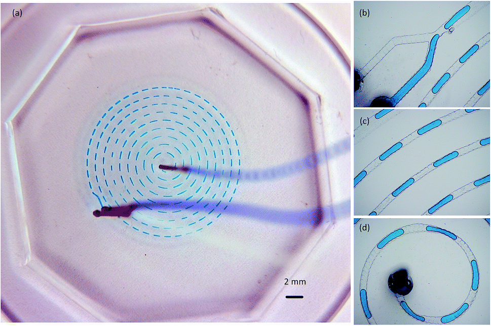 | ||
| Fig. 8 Generation of blue dyed water droplets in corn oil with the spiral micro channel at a feed speed of 2 μL min−1, (a) global view, (b) pressure induced breaking of water in the inlet area, (c) spiral flow of the droplets, (d) outlet area. | ||
3D printed network microfluidic chip
A network microflow was produced on 3D replicated PDMS micro channels (Fig. 9). The channel width on the 3D CAD model was 0.2 mm, and the model was sliced without filling paths. The sliced layer thickness (Ds) was 50 μm. The top surface of the CAD modeled bridge was 4 mm from the bottom, and the resulting wax bridge height was 3.5 mm. Blue and yellow dyes flowed smoothly without interfering with each other at a feed speed of 100 μL min−1. This chip provided a very promising method for the functional 3D microfluidic micro total analysis. | ||
| Fig. 9 Network 3D microfluidic chip replicated with 3D printed wax mold, (a) network flow of blue and yellow dyes at a feed speed of 100 μL min−1 respectively, (b) a junction in the network microfluidic chip. | ||
Conclusion
In this paper we demonstrated a novel method for the fabricating 3D PDMS microfluidic chips with a modified, open-source FDM 3D printer. The wax droplets were generated with a PZT actuator and a glass nozzle. The glass nozzle was inexpensive and easily prepared. The wax material was low cost and freely available. The 3D printed wax mold could be clearly removed from the cured PDMS. Micro-jetting based 3D printing has the advantage of high resolution, non-contact, and convenience for fabricating micro pillars or networks because the wax material can be totally sacrificed. With this modified 3D wax printer, real 3D wax structures such as a spiral growing square shell, a 3D letter, and arc bridges could be prepared. Passive micromixing, micro water in oil droplet generation, and network flowing were demonstrated with the replicated 3D PDMS microfluidic chips. Compared with the conventional methods of photolithography and femtosecond laser, this method was low cost and real 3D fluid channel could be accomplished on PDMS. This study demonstrated a rapid and easy method to develop 3D microfluidic chips and assist 3D chemical and biological functional microfluid analysis.Acknowledgements
This paper is supported by the Fundamental Research Funds for the Central Universities, the Postdoctoral Science Foundation of Jiangsu Province (No. 1601010B), the Key Technology RD Program of Jiangsu Province (No. BE2016010), the National Natural Science Foundation of China (No. 61273243, No. 51407095), the Natural Science Foundation of Jiangsu Province (No. BK20150973). Scientific Research Innovation Program for Graduate of Jiangsu Province (No. SJLX16_0282), the Science and Technology Achievement Transformation Foundation of Jiangsu Province (No. BA2016106).References
- A. Manz, N. Graber and H. M. Widmer, Miniaturized total chemical analysis systems: a novel concept for chemical sensing, Sens. Actuators, B, 1990, 1(1), 244–248 CrossRef CAS.
- S. Dhanekar, S. Chandra and R. Balasubramaniam, Micro-mixer device with deep channels in silicon using modified RIE process: fabrication, packaging and characterization, Microsyst. Technol., 2016, 22(3), 515–522 CrossRef CAS.
- E. Y. Kenig, Y. Su, A. Lautenschleger, P. Chasanis and M. Grünewald, Micro-separation of fluid systems: a state-of-the-art review, Sep. Purif. Technol., 2013, 120, 245–264 CrossRef CAS.
- A. S. Yang, F. C. Chuang, C. K. Chen, M. H. Lee, S. W. Chen, T. L. Su and Y. C Yang, A high-performance micromixer using three-dimensional Tesla structures for bio-applications, Chem. Eng. J., 2015, 263, 444–451 CrossRef CAS.
- J. El-Ali, P. K. Sorger and K. F. Jensen, Cells on chips, Nature, 2006, 442(7101), 403–411 CrossRef CAS PubMed.
- S. Jang, B. Lee, H. H. Jeong, S. H. Jin, S. Jang, S. G. Kim, G. Y. Jung and C. S. Lee, On-chip analysis, indexing and screening for chemical producing bacteria in a microfluidic static droplet array, Lab Chip, 2016, 16(10), 1909–1916 RSC.
- Z. Li, A. M. Leshansky, L. M. Pismen and P. Tabeling, Step-emulsification in a microfluidic device, Lab Chip, 2015, 15(4), 1023–1031 RSC.
- R. Hu, P. Liu, P. Chen, L. Wu, Y. Wang, X. Feng and B. F. Liu, Encapsulation of single cells into monodisperse droplets by fluorescence-activated droplet formation on a microfluidic chip, Talanta, 2016, 153, 253–259 CrossRef CAS PubMed.
- H. N. Chan, Y. Chen, Y. Shu, Y. Chen, Q. Tian and H. Wu, Direct, one-step molding of 3D-printed structures for convenient fabrication of truly 3D PDMS microfluidic chips, Microfluid. Nanofluid., 2015, 1–10 CAS.
- Y. C. Lin, C. C. Lee, H. S. Lin, Z. H. Hong, F. C. Hsu, T. P. Hung and Y. T. Lyu, Fabrication of microfluidic structures in quartz via micro machining technologies, Microsyst. Technol., 2015, 1–9 Search PubMed.
- X. Wang, C. Liedert, R. Liedert and I. Papautsky, A disposable, roll-to-roll hot-embossed inertial microfluidic device for size-based sorting of microbeads and cells, Lab Chip, 2016, 16(10), 1821–1830 RSC.
- Y. He, W. Wu, T. Zhang and J. Fu, Micro structure fabrication with a simplified hot embossing method, RSC Adv., 2015, 5(49), 39138–39144 RSC.
- C. Szydzik, B. Niego, G. Dalzell, M. Knoerzer, F. Ball, W. S. Nesbitt, R. L. Medcalfb, K. Khoshmanesha and A. Mitchell, Fabrication of complex PDMS microfluidic structures and embedded functional substrates by one-step injection moulding, RSC Adv., 2016, 6(91), 87988–87994 RSC.
- Y. Li and S. Qu, Water-assisted femtosecond laser ablation for fabricating three-dimensional microfluidic chips, Curr. Appl. Phys., 2013, 13(7), 1292–1295 CrossRef.
- Z. Isiksacan, M. T. Guler, B. Aydogdu, I. Bilican and C. Elbuken, Rapid fabrication of microfluidic PDMS devices from reusable PDMS molds using laser ablation, J. Micromech. Microeng., 2016, 26(3), 035008 CrossRef.
- K. Iwai, K. C. Shih, X. Lin, T. A. Brubaker, R. D. Sochol and L. Lin, Finger-powered microfluidic systems using multilayer soft lithography and injection molding processes, Lab Chip, 2014, 14(19), 3790–3799 RSC.
- Y. Xia and G. M. Whitesides, Soft lithography, Annu. Rev. Mater. Sci., 1998, 28(1), 153–184 CrossRef CAS.
- W. Yue, C. W. Li, T. Xu and M. Yang, Screen printing of solder resist as master substrates for fabrication of multi-level microfluidic channels and flask-shaped microstructures for cell-based applications, Biosens. Bioelectron., 2013, 41, 675–683 CrossRef CAS PubMed.
- A. Grimes, D. N. Breslauer, M. Long, J. Pegan, L. P. Lee and M. Khine, Shrinky-Dink microfluidics: rapid generation of deep and rounded patterns, Lab Chip, 2008, 8(1), 170–172 RSC.
- M. Abdelgawad, M. W. Watson, E. W. Young, J. M. Mudrik, M. D. Ungrin and A. R. Wheeler, Soft lithography: masters on demand, Lab Chip, 2008, 8(8), 1379–1385 RSC.
- M. T. Koesdjojo, C. R. Koch and V. T. Remcho, Technique for microfabrication of polymeric-based microchips from an SU-8 master with temperature-assisted vaporized organic solvent bonding, Anal. Chem., 2009, 81(4), 1652–1659 CrossRef CAS PubMed.
- Y. Lu, B. Lin and J. Qin, Patterned paper as a low-cost, flexible substrate for rapid prototyping of PDMS microdevices via “liquid molding”, Anal. Chem., 2011, 83(5), 1830–1835 CrossRef CAS PubMed.
- S. Zeinali, B. Çetin, S. N. B. Oliaei and Y. Karpat, Fabrication of continuous flow microfluidics device with 3D electrode structures for high throughput DEP applications using mechanical machining, Electrophoresis, 2015, 36(13), 1432–1442 CrossRef CAS PubMed.
- Y. He, Y. Wu, J. Z. Fu, Q. Gao and J. J. Qiu, Developments of 3D Printing Microfluidics and Applications in Chemistry and Biology: A Review, Electroanalysis, 2016, 28(8), 1658–1678 CrossRef CAS.
- N. Bhattacharjee, A. Urrios, S. Kang and A. Folch, The upcoming 3D-printing revolution in microfluidics, Lab Chip, 2016, 16(10), 1720–1742 RSC.
- A. J. Morgan, L. H. San Jose, W. D. Jamieson, J. M. Wymant, B. Song, P. Stephens and O. K. Castell, Simple and Versatile 3D Printed Microfluidics Using Fused Filament Fabrication, PLoS One, 2016, 11(4), e0152023 Search PubMed.
- P. J. Kitson, M. H. Rosnes, V. Sans, V. Dragone and L. Cronin, Configurable 3D-printed millifluidic and microfluidic ‘lab on a chip’ reactionware devices, Lab Chip, 2012, 12(18), 3267–3271 RSC.
- G. W. Bishop, J. E. Satterwhite, S. Bhakta, K. Kadimisetty, K. M. Gillette, E. Chen and J. F. Rusling, 3D-Printed Fluidic Devices for Nanoparticle Preparation and Flow-Injection Amperometry using Integrated Prussian Blue Nanoparticle-Modified Electrodes, Anal. Chem., 2015, 87(10), 5437–5443 CrossRef CAS PubMed.
- J. Liu, H. H. Hwang, P. Wang, G. Whang and S. Chen, Direct 3D-printing of cell-laden constructs in microfluidic architectures, Lab Chip, 2016, 16(8), 1430–1438 RSC.
- M. P. Lee, G. J. Cooper, T. Hinkley, G. M. Gibson, M. J. Padgett and L. Cronin, Development of a 3D printer using scanning projection stereolithography, Sci. Rep., 2015, 5(9875), 1–5 Search PubMed.
- A. I. Shallan, P. Smejkal, M. Corban, R. M. Guijt and M. C. Breadmore, Cost-effective three-dimensional printing of visibly transparent microchips within minutes, Anal. Chem., 2014, 86(6), 3124–3130 CrossRef CAS PubMed.
- J. L. Erkal, A. Selimovic, B. C. Gross, S. Y. Lockwood, E. L. Walton, S. McNamara and D. M. Spence, 3D printed microfluidic devices with integrated versatile and reusable electrodes, Lab Chip, 2014, 14(12), 2023–2032 RSC.
- K. B. Anderson, S. Y. Lockwood, R. S. Martin and D. M. Spence, A 3D printed fluidic device that enables integrated features, Anal. Chem., 2013, 85(12), 5622–5626 CrossRef CAS PubMed.
- D. P. Parekh, C. Ladd, L. Panich, K. Moussa and M. D. Dickey, 3D printing of liquid metals as fugitive inks for fabrication of 3D microfluidic channels, Lab Chip, 2016, 16(10), 1812–1820 RSC.
- Y. He, J. Qiu, J. Fu, J. Zhang, Y. Ren and A. Liu, Printing 3D microfluidic chips with a 3D sugar printer, Microfluid. Nanofluid., 2015, 19(2), 447–456 CrossRef CAS.
- M. K. Gelber and R. Bhargava, Monolithic multilayer microfluidics via sacrificial molding of 3D-printed isomalt, Lab Chip, 2015, 15(7), 1736–1741 RSC.
- J. S. Miller, K. R. Stevens, M. T. Yang, B. M. Baker, D. H. T. Nguyen, D. M. Cohen and R. Chaturvedi, Rapid casting of patterned vascular networks for perfusable engineered three-dimensional tissues, Nat. Mater., 2012, 11(9), 768–774 CrossRef CAS PubMed.
- V. Saggiomo and A. H. Velders, Simple 3D printed scaffold-removal method for the fabrication of intricate microfluidic devices, Adv. Sci., 2015, 2(9), 1500125 CrossRef PubMed.
- C. Chung, Y. J. Chen, P. C. Chen and C. Y. Chen, Fabrication of PDMS passive micromixer by lost-wax casting, Int. J. Precis. Eng. Manuf., 2015, 16(9), 2033–2039 CrossRef.
- C. C. W. Tse, S. S. Ng, J. Stringer, S. MacNeil, J. W. Haycock and P. J. Smith, Utilising Inkjet Printed Paraffin Wax for Cell Patterning Applications, International Journal of Bioprinting, 2015, 2(1), 1–10 Search PubMed.
- Z. Li, J. Yang, L. Zhu and W. Tang, Fabrication of paper micro-devices with wax jetting, RSC Adv., 2016, 6(22), 17921–17928 RSC.
Footnote |
| † Electronic supplementary information (ESI) available. See DOI: 10.1039/c6ra24884e |
| This journal is © The Royal Society of Chemistry 2017 |