
 Open Access Article
 This Open Access Article is licensed under a Creative Commons Attribution-Non Commercial 3.0 Unported Licence
Atomic layer deposition of Al2O3 on MoS2, WS2, WSe2, and h-BN: surface coverage and adsorption energy†
Taejin Park‡
ab,
Hoijoon Kim‡c,
Mirine Leemc,
Wonsik Ahnc,
Seongheum Choic,
Jinbum Kimab,
Joon Uha,
Keewon Kwonb,
Seong-Jun Jeongd,
Seongjun Parkd,
Yunseok Kim*c and
Hyoungsub Kim*c
aSemiconductor R&D Center, Samsung Electronics, Hwaseong 18488, Republic of Korea
bDepartment of Semiconductor and Display Engineering, Sungkyunkwan University, Suwon 16419, Republic of Korea
cSchool of Advanced Materials Science and Engineering, Sungkyunkwan University, Suwon 16419, Republic of Korea. E-mail: yunseokkim@skku.edu; hsubkim@skku.edu
dNano-Electronics Lab., Devices System Research Center, Samsung Advanced Institute of Technology, Suwon 16678, Republic of Korea
First published on 4th January 2017
Abstract
Uniform deposition of high-k dielectrics on two-dimensional (2D) crystals is highly desirable for their use in future nano-electronic devices. Here, the surface coverage of the Al2O3 films grown by atomic layer deposition (ALD) was investigated on mechanically-exfoliated MoS2, WS2, WSe2, and h-BN flakes for exploring the deposition kinetics of the Al2O3 films on the 2D crystals. The film coverage followed a decreasing order of WSe2 > WS2 > MoS2 > h-BN, which was mainly determined by the ALD temperature and adsorption energy (Eads) of the ALD precursor (trimethyl-aluminum) during the initial ALD cycles. The obtained |Eads| values of the precursor on the 2D crystals corresponded well to a van der Waals physisorption energy of 0.05–0.26 eV. Furthermore, the magnitude of the extracted Eads values showed a strong dependence on the induced dipole polarizability of the 2D crystals. The obtained results demonstrate that the surface coverage of the ALD high-k dielectrics can be modulated by choosing the types of the 2D substrates, and could provide a pathway for the integration of high-k dielectrics in 2D crystal-based nano-electronic devices.
1. Introduction
Since the discovery of an electric field effect in atomically thin graphene layers,1 two-dimensional (2D) crystals have received great attention as a potential nano-scale material for future nano-electronic devices. Among the various 2D crystals, transition metal dichalcogenides have emerged as the most promising candidate for novel semiconductor device applications, such as electronic, optoelectronic, and photonic devices, because of their wide and controllable band gap.2 In addition, h-BN has been recently used as an insulating component in these devices because of its analogous 2D structure with a wide direct band gap.3–5 While each constituting 2D layer has strong covalent/ionic bonds in the in-plane direction, these 2D layers are weakly bound together by a van der Waals (vdW) force, which provides a handle to manipulate their electrical and optical properties by engineering the number of stacked layers.2–5Because of the weak bonding, a layered structure of 2D crystals enables easy cleavage and isolation of a few layered specimens using an adhesive tape, and for a decade, most researches have focused on paving the way for their potential applications using the mechanically exfoliated 2D flakes.1,2 Furthermore, to achieve commercially available 2D devices in the future, there have been many attempts to develop wafer-scale synthesis of several 2D films6–8 and also to integrate high-k dielectrics on their surfaces.9–12 However, several studies have demonstrated that uniform and conformal deposition of ultra-thin high-k dielectrics using atomic layer deposition (ALD) was not guaranteed on these 2D materials because of the lack of available sites for chemisorption of an ALD precursor on their surface,10–12 similar to the case on the graphene surface.13,14 Consequently, the ALD precursor is attached to a 2D crystal surface with a much smaller physisorption energy (Ephys) than chemisorption energy (Echem), and can be easily detached via thermal desorption during precursor injection and/or the following purging step,15,16 which leads to a non-uniform film formation with many uncovered regions (see Fig. 1).
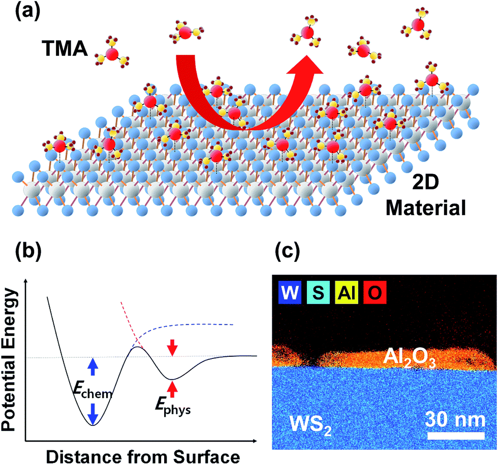 | ||
| Fig. 1 (a) Schematic diagram showing the adsorption/desorption processes of TMA precursors during the initial ALD process on the 2D crystal surface. (b) Potential-well model describing the chemisorption and physisorption of an ALD precursor on the substrate surface. The easy desorption of TMA molecules attached with a weak physisorption energy (Ephys) on the 2D crystal surface often results in non-uniform film formation, as demonstrated in the energy-dispersive X-ray spectroscopy mapping image of (c), where ALD-Al2O3 (∼10 nm) was deposited on WS2 at 250 °C. | ||
In order to understand the ALD kinetics of the high-k dielectrics on the 2D crystals in more detail and also to develop a method to achieve uniform film formation, the adsorption energy (Eads) of the ALD precursors on 2D material substrates needs to be examined and compared. Although the surface energies of several 2D materials were experimentally extracted by several researchers using various routes (spectroscopic,10 wetting angle,17 and solvent dispersion experiments18), a few theoretical Eads values were reported only via computational quantum simulation using a density functional theory, e.g., the Eads of trimethyl-aluminum (TMA) on MoS2 and h-BN surfaces.12
Here, we investigated the deposition characteristics of the ALD-Al2O3 films on several 2D materials including MoS2, WS2, WSe2, and h-BN. Moreover, the ALD-Al2O3 film coverage was quantified as a function of the ALD temperature, and the Eads of a TMA molecule on the 2D crystal surfaces were experimentally extracted and compared for a better understanding of the ALD kinetics.
2. Experimental
2.1 Preparation of 2D crystal substrates
Several 2D flakes (MoS2, WS2, WSe2, and h-BN) were exfoliated from the extracted minerals (>99.995%, HQ graphene) using an adhesive tape and transferred onto an oxidized Si wafer. The specimens were soaked in acetone for 8 h to remove remnant sticky organics, and rinsed with acetone, methanol, and isopropanol for 30 s each. The lateral diameter and thickness of the transferred flakes were observed to be 5–10 μm and more than 30 nm, respectively.2.2 ALD and film characterization
ALD-Al2O3 films were deposited on the exfoliated/transferred 2D flakes at different temperatures (150, 200, and 250 °C) using TMA (>99.99%, UP Chemical) and deionized H2O. TMA [10 standard cubic centimeters per minute (sccm)] and H2O (10 sccm) were injected alternately into a chamber for 1.0 s and 1.5 s, respectively. The purge steps consisted of 200 sccm N2 flow for 20 s and 30 s directly after TMA and H2O injections, respectively. Uniform deposition of the Al2O3 film was separately verified on a Si substrate, as shown in Fig. S1 in the ESI.† The deposition feature and coverage of the ALD-Al2O3 films on the 2D flakes were analyzed by high resolution transmission electron microscopy (HRTEM, JEOL, ARM-200F), atomic force microscopy (AFM, Hitachi, 5300E), and scanning electron microscopy (SEM, JEOL, JSM-6390A).3. Results and discussion
3.1 Surface coverage of ALD-Al2O3 on MoS2, WS2, WSe2, and h-BN
First, to examine the dependence of the deposition temperature on the surface coverage, thick ALD-Al2O3 films (with a thickness of approximately 10 nm) were deposited on the exfoliated/transferred MoS2, WS2, WSe2, and h-BN flakes at 150, 200, and 250 °C. Because the Al2O3 deposition rate slowly decreased with increasing substrate temperature, the number of ALD cycles was varied to yield a similar thickness at different temperatures. Fig. S2 in the ESI† presents the cross-sectional TEM images obtained from selected local areas where the exfoliated flake surfaces were fully covered with a thick ALD-Al2O3 film deposited at 250 °C. The cross-sectional view of the 2D flakes exhibited their layered structure, and Al2O3 deposition on top, with an expected thickness of ∼10 nm, was confirmed.For a detailed analysis of the surface feature of the thick ALD-Al2O3 films, AFM measurements were performed on a more extensive scanning area of 1.0 μm × 1.0 μm and their topographic surface images are shown in Fig. 2. As can be inferred from the AFM images, an increase in the ALD temperature significantly reduced the Al2O3 coverage on all the 2D substrates because of the augmented thermal desorption of the precursors during the ALD process, as addressed in previous reports.10–12 Except on h-BN, a nearly conformal deposition of the Al2O3 films was achieved on MoS2, WS2, and WSe2 at the lowest ALD temperature of 150 °C without any observable crevice in the AFM topography images; however, this cannot guarantee the absence of pinholes in the film, which can induce a dielectric leakage current.
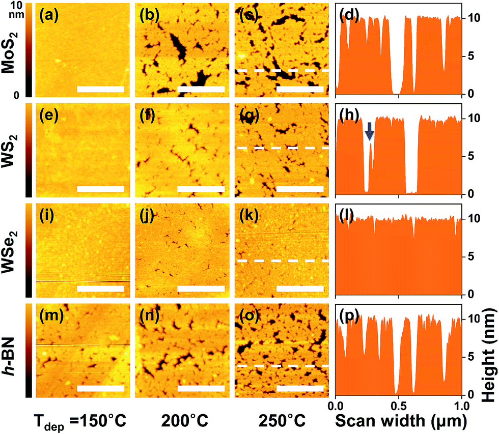 | ||
| Fig. 2 AFM topography images and line (height) profiles of the thick ALD-Al2O3 films (∼10 nm) deposited on (a–d) MoS2, (e–h) WS2, (i–l) WSe2, and (m–p) h-BN flakes at various temperatures (150, 200, and 250 °C). The scale bar is 500 nm. The line profiles (d, h, l and p) were obtained from the dashed lines of AFM topography images at 250 °C. The blue arrow shown in (h) indicates a shoulder structure. | ||
The AFM line (height) profiles shown in Fig. 2(d), (h), (l) and (p) revealed detailed information on the ALD-Al2O3 deposition characteristics on several 2D flake surfaces. They were extracted from the dashed lines in the AFM topography images of the 250 °C samples [Fig. 2(c), (g), (k) and (o)] that have the lowest film coverage at different ALD temperatures. On the uniformly coated regions, the Al2O3 thickness measured using AFM (the height difference between the surface and the lowest bottom of crevices) was identical to that measured using TEM. However, variously shaped crevices were found, e.g., deep with a wide width and shallow with a small width. The small and shallow crevices might be formed by a concurrent lateral growth of ALD-Al2O3 because of a good step-coverage characteristic of the ALD. In the case of the large crevice, its dimension is over 100 nm, which is too large to be filled by lateral film growth and indicates an insufficient nucleation process on the 2D surface throughout the ALD process. Although a few sites exhibited a crevice shape with a shoulder that might have nucleated and grown in the middle of the ALD process, as indicated by a blue arrow in Fig. 2(h), the overall film growth after a few cycles of initial ALD preferred the surface of the nucleated Al2O3 rather than the virgin 2D surface only with a weak vdW force.
3.2 Eads of TMA on MoS2, WS2, WSe2, and h-BN
Typically, the ALD process builds up a film through sub-monolayer adsorption of gaseous precursors on the substrate, followed by a chemical reaction [2Al(CH3)3 + 3H2O → Al2O3 + 6CH4 in this experiment] with the subsequently introduced other precursor.15,16 Therefore, chemisorption of reactants promises rigid and uniform film growth, while physisorption does not allow it since the weakly bonded reactants can be easily detached from the substrate via their thermal desorption during precursor injection and/or the following purging step.15,16 Under these circumstances, the 2D crystal surface with a small surface energy often yields many uncovered regions, i.e., crevices and pinholes, in the ALD film.10–14 Moreover, the continuing ALD cycles might hardly provide nucleation sites for the subsequent growth on the exposed surface through the crevices because the Al2O3 deposited initially could attract the ALD reactants more strongly than the virgin 2D crystal surface, by the same logic. As a consequence, because a few initial cycles of the ALD process might mostly determine the final film coverage,12 specifically, stronger adsorption of an ALD precursor on the 2D flakes can suppress the subsequent desorption and provide higher film coverage.In order to assess the adsorption and desorption rates at the initial stage of the ALD process, which is the predominant factor affecting the final film coverage, the ALD of Al2O3 was performed on the 2D substrates for 10 cycles as a function of the deposition temperature. The resulting plan-view SEM images of the initial film features are presented in Fig. 3. Considering the deposition rate, the film thickness was estimated to be about 0.9–1.1 nm depending on the ALD temperature. For the SEM images, the bright and dark areas present regions with and without the Al2O3 film, respectively. However, for the h-BN sample, the image contrast was reversed because of a greater charging effect on the insulating h-BN surface than the substrate (SiO2 on Si). The surface coverage of the thin Al2O3 films on several 2D flakes was quantified using an image-processing software,19 which can count the number of pixels after converting a gray-colored SEM image to a binary contrast image (Fig. S3†). The quantified film coverage of the thin Al2O3 films exhibited a decreasing trend with increasing deposition temperature and followed a substrate dependence in the order WSe2 > WS2 > MoS2 > h-BN, as shown in Fig. 4(a). When the quantification process was applied to the AFM data shown in Fig. 2, similar decreasing trends were also observed for the thick Al2O3 (∼10 nm) deposition case; the detailed quantification process using AFM data and its results can be found in Fig. S4 and Table S1.†
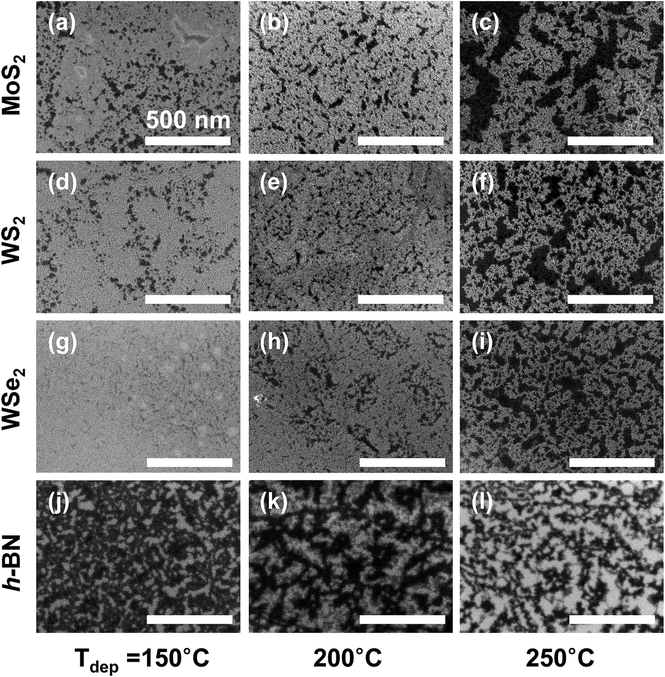 | ||
| Fig. 3 SEM images of the thin ALD-Al2O3 films (0.9–1.1 nm) deposited on (a–c) MoS2, (d–f) WS2, (g–i) WSe2, and (j–l) h-BN flakes at various temperatures (150, 200, and 250 °C). The scale bar is 500 nm. | ||
 | ||
| Fig. 4 (a) Surface coverage of the thin ALD-Al2O3 films (0.9–1.1 nm) deposited on MoS2, WS2, WSe2, and h-BN flakes at various temperatures (150, 200, and 250 °C) measured using SEM. The solid lines are a guide to the eye. (b) ln(1 − θ) vs. 1/kBT plot used for extraction of adsorption energy (Eads) by linear fitting. The solid lines are linear fits to the data. | ||
As mentioned above, the ALD film growth occurs through precursor adsorption and its reaction with the subsequently introduced precursor. Therefore, if the precursor desorption is facilitated on the 2D crystal surface, the film coverage will decrease. If we assume that a few cycles of ALD in the initial process contribute little to lateral film growth, the resulting film coverage will be primarily determined by competition between the adsorption and desorption rates of the ALD precursors. According to the Langmuir adsorption model dealing with the adsorption kinetics between gas and solid, the time-dependent change in the surface coverage can be expressed as dθ/dt = kadsP(1 − θ) − kdesθ, where θ is the surface coverage of the adsorbed gas molecules, t is time, and P is the pressure.16,20,21 In addition, kads and kdes are the adsorption and desorption rate constants, respectively, which have a temperature (T) dependence of kads ∼ exp(−Eads/kBT) and kdes ∼ exp(−Edes/kBT).16,22–24 Here, Eads, Edes, and kB are the adsorption energy, desorption energy, and Boltzmann constant, respectively. The gaseous impingement generates adsorbates on an unoccupied fraction of 1 − θ at the rate of kads,16,23 and at the same time, the adsorbates on an occupied fraction of θ experience desorption at the rate of kdes. In terms of Edes, the chemisorption process requires an additional energy to dissociate the chemical bonds;16,22,23 however, the physisorption process does not require more energy than Eads (Ephys in Fig. 1). Therefore, Edes ≈ −Eads can be reasonably assumed for the initial ALD process on the chemically inert 2D crystal surface.16,22
Based on the adsorption and desorption theory of gas molecules on a chemically inert solid surface discussed above, we simplify the coverage mechanism of the initial Al2O3-ALD process as follows. The adsorption/desorption processes of TMA can be assumed to be the most dominant in determining the initial surface coverage; according to the theoretical calculation by Liu et al.,12 the |Eads| of H2O is much smaller than that of TMA, so that H2O is hardly adsorbed and easily desorbed from 2D crystals such as MoS2 and h-BN.
The adsorption of TMA molecules is primarily affected by T (of a precursor), P, and Eads, where Eads is the only variable dependent on the type of 2D substrates. Meanwhile, the adsorbed TMA molecules experience subsequent desorption governed by two variables of T (of a substrate) and Edes, which eventually determines the Al2O3 coverage. In these circumstances, the Eads (≈Edes) can be experimentally estimated solely by the substrate temperature (T) variable because the uncovered fraction (1 − θ) is proportional to exp(−Edes/kBT).21–24 Fig. 4(b) shows the ln(1 − θ) vs. 1/kBT plots for different 2D substrates with the |Eads| values extracted from the slope of the linearly fitted lines; the detailed fitting results are also included in Table S2.† Here, the film coverage measured using SEM was used to calculate the 1 − θ values. The extracted |Eads| values were below 0.26 eV for all the samples, which are reasonably smaller than the 1.13 eV of the reported |Eads| for TMA chemisorption on a hydroxylated Al2O3 substrate.25 Moreover, these values correspond well to the general values for vdW physisorption of various gases on a metal surface (0.21–0.25 eV (ref. 16 and 23) or <0.4 eV (ref. 22)). Our experimentally obtained values might have a little deviation from the ideal values, because they were deduced after fixing the number of ALD cycles, and contaminants or defects on the 2D surface might have an additional effect on the film coverage.9,14 As shown in Fig. 4(b), the |Eads| values strongly depended on the 2D substrates, exhibiting the order WSe2 > WS2 > MoS2 > h-BN, with a maximum value of 0.26 eV and a minimum value of 0.05 eV for WSe2 and h-BN, respectively. This decreasing trend matches well with the order of surface energies of the 2D crystals deduced by wettability and film coverage measurement results.12,17
The Eads of vdW physisorption is related to a dipolar interaction between the 2D substrate and the ALD precursor, which originates from the Keesom, Debye, and London forces depending on the respective contribution of the permanent and induced dipoles.26 In our experimental case, because no permanent dipole is expected to exist for the vertically symmetric structure of 2D crystals in a surface normal direction and identical ALD precursors were used for all the samples, we can postulate that the observed order of Eads values by the vdW physisorption might be mainly governed by the magnitude of induced-dipole polarizability of the 2D substrate itself. For the 2D crystals used in this experiment, the induced polarization originates from the electronic and the atomic/ionic factors, which represent the displacement of the outer electron clouds and the local distortion of the atomic bond, respectively.27 Therefore, because a large polarization is expected when the atomic number and radius increase,27 W-compounds and Se-compounds would have larger induced polarization than Mo and S compounds, respectively. In addition, a relatively weak polarization is expected in B and N compounds. The strong polarization can increase the |Eads|, and thus increase the film coverage when no chemisorption is involved during ALD. These assumptions predict the order of polarizability of 2D substrates and |Eads| values of TMA on 2D substrates as WSe2 > WS2 > MoS2 > h-BN, which explains the order of ALD-Al2O3 film coverage observed in our experiment well. This indicates that the uniform and conformal deposition of the high-k dielectrics can be strongly affected by the atomic number and radius of the elements in the 2D substrates, influencing the Eads values of the ALD precursors.
4. Conclusion
We have reported the deposition kinetics of ALD-Al2O3 films on the 2D crystal surfaces. According to the surface coverage measurement of the ALD-Al2O3 films on several 2D crystals including MoS2, WS2, WSe2, and h-BN, the film coverage decreased as the ALD temperature increased and showed the order WSe2 > WS2 > MoS2 > h-BN at the same temperature. By applying the adsorption/deposition kinetics to the early ALD stage, the Eads values of TMA on several 2D crystal surfaces were extracted through an experimental route by examining the dependence of film coverage on the ALD temperature. The extracted |Eads| values were in the range of 0.05–0.26 eV depending on the identity of the 2D crystal and corresponded well to the typical vdW physisorption values. Moreover, the order of |Eads| values showed a strong dependence on the type of 2D crystals, which is correlated with the induced polarizability of the 2D crystals governed by the atomic number and radius of their constituting elements. The obtained results indicate that the surface coverage of the high-k dielectrics on the 2D crystals can be modulated by choosing the types of 2D substrates with different Eads values. Eventually, it could offer an important clue in understanding the ALD kinetics on different 2D crystal surfaces and finding a solution for successful integration of the high-k dielectrics on them.Acknowledgements
This work was supported by a Basic Research Lab program through the National Research Foundation of Korea funded by the Ministry of Science, ICT & Future Planning (NRF-2014R1A4A1008474).References
- K. S. Novoselov, A. K. Geim, S. V. Morozov, D. Jiang, Y. Zhang, S. V. Dubonos, I. V. Grigorieva and A. A. Firsov, Science, 2004, 306, 666–669 CrossRef CAS PubMed.
- Q. H. Wang, K. Kalantar-Zadeh, A. Kis, J. N. Coleman and M. S. Strano, Nat. Nanotechnol., 2012, 7, 699–712 CrossRef CAS PubMed.
- Y. Kubota, K. Watanabe, O. Tsuda and T. Taniguchi, Science, 2007, 317, 932–934 CrossRef CAS PubMed.
- Z. Liu, L. Ma, G. Shi, W. Zhou, Y. Gong, S. Lei, X. Yang, J. Zhang, J. Yu, K. P. Hackenberg, A. Babakhani, J. C. Idrobo, R. Vajtai, J. Lou and P. M. Ajayan, Nat. Nanotechnol., 2013, 8, 119–124 CrossRef CAS PubMed.
- W.-Q. Han, L. Wu, Y. Zhu, K. Watanabe and T. Taniguchi, Appl. Phys. Lett., 2008, 93, 223103 CrossRef.
- J. Yang, Y. Gu, E. Lee, H. Lee, S. H. Park, M. H. Cho, Y. H. Kim, Y. H. Kim and H. Kim, Nanoscale, 2015, 7, 9311–9319 RSC.
- B. Wang, C. Muratore, A. A. Voevodin and M. A. Haque, Nano Convergence, 2014, 1, 22 CrossRef.
- Y. H. Lee, X. Q. Zhang, W. Zhang, M. T. Chang, C. T. Lin, K. D. Chang, Y. C. Yu, J. T. Wang, C. S. Chang, L. J. Li and T. W. Lin, Adv. Mater., 2012, 24, 2320–2325 CrossRef CAS PubMed.
- C. Wirtz, T. Hallam, C. P. Cullen, N. C. Berner, M. O'Brien, M. Marcia, A. Hirsch and G. S. Duesberg, Chem. Commun., 2015, 51, 16553–16556 RSC.
- S. McDonnell, B. Brennan, A. Azcatl, N. Lu, H. Dong, C. Buie, J. Kim, C. L. Hinkle, M. J. Kim and R. M. Wallace, ACS Nano, 2013, 7, 10354–10361 CrossRef CAS PubMed.
- H. Liu and P. D. Ye, IEEE Electron Device Lett., 2012, 33, 546–548 CrossRef CAS.
- H. Liu, K. Xu, X. Zhang and P. D. Ye, Appl. Phys. Lett., 2012, 100, 152115 CrossRef.
- Y. Zhang, Z. Qiu, X. Cheng, H. Xie, H. Wang, X. Xie, Y. Yu and R. Liu, J. Phys. D: Appl. Phys., 2014, 47, 055106 CrossRef.
- X. Wang, S. M. Tabakman and H. Dai, J. Am. Chem. Soc., 2008, 130, 8152–8153 CrossRef CAS PubMed.
- T. Kääriäinen, D. Cameron, M.-L. Kääriäinen and A. Sherman, Atomic Layer Deposition: Principles, Characteristics, and Nanotechnology Applications, John Wiley & Sons, New Jersey, 2nd edn, 2013 Search PubMed.
- M. Ohring, Materials Science of Thin Films, Academic press, New Jersey, 2nd edn, 2001 Search PubMed.
- M. Annamalai, K. Gopinadhan, S. A. Han, S. Saha, H. J. Park, E. B. Cho, B. Kumar, A. Patra, S. W. Kim and T. Venkatesan, Nanoscale, 2016, 8, 5764–5770 RSC.
- G. Cunningham, M. Lotya, C. S. Cucinotta, S. Sanvito, S. D. Bergin, R. Menzel, M. S. P. Shaffer and J. N. Coleman, ACS Nano, 2012, 6, 3468–3480 CrossRef CAS PubMed.
- https://imagej.nih.gov/ij/index.html, accessed Septemper 2016.
- I. Langmuir, J. Am. Chem. Soc., 1918, 40, 1361–1403 CrossRef CAS.
- J. Hudson, Surface Science: An Introduction, Butterworth-Heinemann, Boston, 2013 Search PubMed.
- K. Jousten, Handbook of Vacuum Technology, Wiley-VCH, Weinheim, 2nd edn, 2008 Search PubMed.
- P. Atkins and J. De Paula, Atkins' Physical Chemistry, Oxford University Press, Oxford, 10th edn, 2014 Search PubMed.
- P. A. Redhead, Vacuum, 1962, 12, 203–211 CrossRef CAS.
- T. Weckman and K. Laasonen, Phys. Chem. Chem. Phys., 2015, 17, 17322–17334 RSC.
- C. J. Van Oss, Interfacial Forces in Aqueous Media, CRC press, Boca Raton, 2006 Search PubMed.
- K. C. Kao, Dielectric Phenomena in Solids, Elsevier academic press, London, 2004 Search PubMed.
Footnotes |
| † Electronic supplementary information (ESI) available: AFM topography image of an ALD-Al2O3 film on Si and TEM images, binary contrast SEM images, AFM-measured surface roughness, and parameters extracted from the SEM-measured surface coverage of the Al2O3 films on 2D flakes. See DOI: 10.1039/c6ra24733d |
| ‡ These authors contributed equally to this work. |
| This journal is © The Royal Society of Chemistry 2017 |