
Rhenium dichalcogenides (ReX2, X = S or Se): an emerging class of TMDs family
Muhammad
Hafeez
ab,
Lin
Gan
a,
Arshad
Saleem Bhatti
b and
Tianyou
Zhai
 *a
*a
aState Key Laboratory of Material Processing and Die & Mould Technology, School of Materials Science and Engineering, Huazhong University of Science and Technology (HUST), Wuhan 430074, P. R. China. E-mail: zhaity@hust.edu.cn
bCentre for Micro and Nano Devices, Department of Physics, COMSATS Institute of Information Technology, Islamabad 44000, Pakistan
First published on 1st March 2017
Abstract
The two-dimensional transition metal dichalcogenides (TMDs) have been attracting increasing interest due to their unique structures and remarkable properties. As a new member of the TMDs family, rhenium dichalcogenides (ReX2, X = S or Se) possess many distinctive features because of an unusually distorted octahedral (1T) crystal structure with triclinic symmetry. In this unique crystal structure, each monolayer contains diamond-shaped chains (DS-chains) comprising interlinked Re4 clusters, which makes the structure anisotropic. This novel structure renders ReX2 with wide applications in (opto-)electronics, such as photodetectors and field effect transistors (FETs). ReX2 are new materials, so this review presents mainly basic and research work done in recent years. In the first part, the unique crystal and electronic structures are introduced. The second part summarizes the various growth methods for ReX2. Finally, the third part focuses on the applications in high-performance photodetectors and FETs based on 2D ReX2.
 Muhammad Hafeez | Dr Muhammad Hafeez is an Assistant Professor in the Department of Physics, COMSATS Institute of Information Technology (CIIT), Islamabad, Pakistan. In 2005, he received his BS degree from the University of Punjab (Lahore, Pakistan). He completed his MS (physics) in 2009 and received his doctorate (physics) in 2013 from the Department of Physics of CIIT under the supervision of Professor Arshad Bhatti. In 2014, he joined the School of Materials Science and Engineering of Huazhong University of Science and Technology (HUST), Wuhan, China, as a postdoctoral fellow. His research interest focus on the controllable scalable synthesis of 2D TMDc via CVD methods for electronic and optoelectronic applications. |
 Lin Gan | Lin Gan received his BS degree in chemistry from Wuhan University in 2005, and then received his doctorate in physical chemistry from Peking University under the supervision of Professor Xuefeng Guo in 2012. Currently, he is working at the School of Materials Science and Engineering, Huazhong University of Science and Technology (HUST). His research interest focuses mainly on the chemical-vapor deposition synthesis of two-dimensional (2D) nanomaterials such as graphene and TMDs, and on the electronic/optoelectronic properties and applications of these 2D materials. |
 Arshad Saleem Bhatti | Arshad Bhatti is a tenured professor of Physics at the COMSATS Institute of Information Technology. Bhatti received his first degree in physics from the University of the Punjab (Lahore, Pakistan) in 1987. He did an MPhil and doctorate in microelectronics and optoelectronics under the supervision of Dr Howard P. Hughes from the University of Cambridge (Cambridge, UK) in 1992 and 1995, respectively. He also did postdoctoral work at the University of Rome (Rome, Italy) from 1998 to 2000 with Professor A. Frova, at the University of Nottingham (Nottingham, UK) from 2000 to 2001, and with Professor L. Eaves at the University of Illinois (Urbana Champaign, Urbana, USA). His research interests include the synthesis and characterization of low-dimensional semiconductor structures for applications in biophysics and the environment. He has published more than 75 papers. He is also a team leader for CIIT in A Large Ion Collider Experiment (ALICE) at CERN. For his services, the Government of Pakistan bestowed him with Tamgha-e-Imtiaz in 2011. |
 Tianyou Zhai | Tianyou Zhai received his BS degree in chemistry from Zhengzhou University in 2003, and then received his doctorate in physical chemistry from the Institute of Chemistry, Chinese Academy of Sciences (ICCAS), under the supervision of Professor Jiannian Yao in 2008. He joined the National Institute for Materials Science (NIMS) as a JSPS postdoctoral fellow of Professor Yoshio Bando's group and then as an ICYS-MANA researcher within NIMS. Currently, he is a Chief Professor of the School of Materials Science and Engineering, Huazhong University of Science and Technology (HUST). His research interests include the controlled synthesis and exploration of fundamental physical properties of inorganic functional nanomaterials, as well as their promising applications in energy science, electronics and optoelectronics. He has authored and co-authored ≈140 peer-reviewed journal articles, five book chapters, co-edited one book on nanotechnology, and held seven patents. His publications have been cited more than 6500 times (H-index is 45). |
Introduction
Graphene has triggered a wave of research interest in ultrathin two-dimensional (2D) transition metal dichalcogenides (TMDs).1–10 TMDs are compounds of the general form MX2, where M denotes a transition metal (Mo, W, Ti, Hf, Re) and X denotes a chalcogen (S, Se, Te).11,12 The variety of TMDs covers a wide range from semiconductors to semi-metals/metals and even super-conductors due to the presence of unsaturated d-orbitals of transition metal.13In particular, atomically thin 2D TMDs are potentially ideal for eliminating short-channel effects, such as drain-induced barrier lowering (DIBL) in metal oxide semiconductor field-effect transistors (MOSFETs).14 Therefore, TMDs could have applications of charge density waves,15 logic transistors,16,17 optoelectronics18–20 and interband tunnel FETs.21–23
Rhenium dichalcogenides (ReX2) are new members among the TMDs family and possess the same typical “sandwich” structure like other TMDs,24–29e.g. MoS2,13,22,30 WS2,31,32 MoSe233,34 and WSe2.35,36 However, ReX2 are unique in that they have much weak interlayer coupling resulting from a distorted octahedral (1T) crystal structure with triclinic symmetry, which renders ReX2 many novel properties, such as anisotropic electronic, optical and mechanical properties.26,28,29,37–39 In this context, we present a comprehensive review about the ReX2 which mainly focus on their various interesting physical properties (crystal structures, electronic structures), followed by their synthetic methods, including bulk crystal growth, chemical exfoliation and vapor-deposition methods. Furthermore, recent reports about the application of these 2D ReX2 into devices (photodetectors, FETs) are presented. Finally, this review is summarized with prospects for future research in this area.
Crystal structure
ReX2 are known to have a layered atomic structure like graphene and other TMDs. Fig. 1a shows the side and top view of single layer of the distorted 1T structure of a ReX2,37,40–42 which is different from the conventional 1H structure of TMDs such as MoS223,43,44 and WS245etc. The crystal structure of ReX2 is very special due to their in-plane motif of diamond-shaped chains (DS-chains) arranged in parallel, as can be seen in the side and top view (Fig. 1a) of the crystal structure.37,46–48Fig. 1b shows an annular dark field (ADF) image of exfoliated ReS2 flakes with mono and trilayer regions where the single-layer region exhibits clearly a DS phase. It is clear from the ADF image of the single layer region that four Re atoms are arranged in a diamond-like shape, and the diamonds form atomic chains in the b direction, as mentioned in Fig. 1b. These structures are clearly visible in the typical ADF images of single-layer ReS2 and trilayer ReSe2 (Fig. 1c and d). The lattice parameters determined using density functional theory (DFT) calculations are presented in Table 1.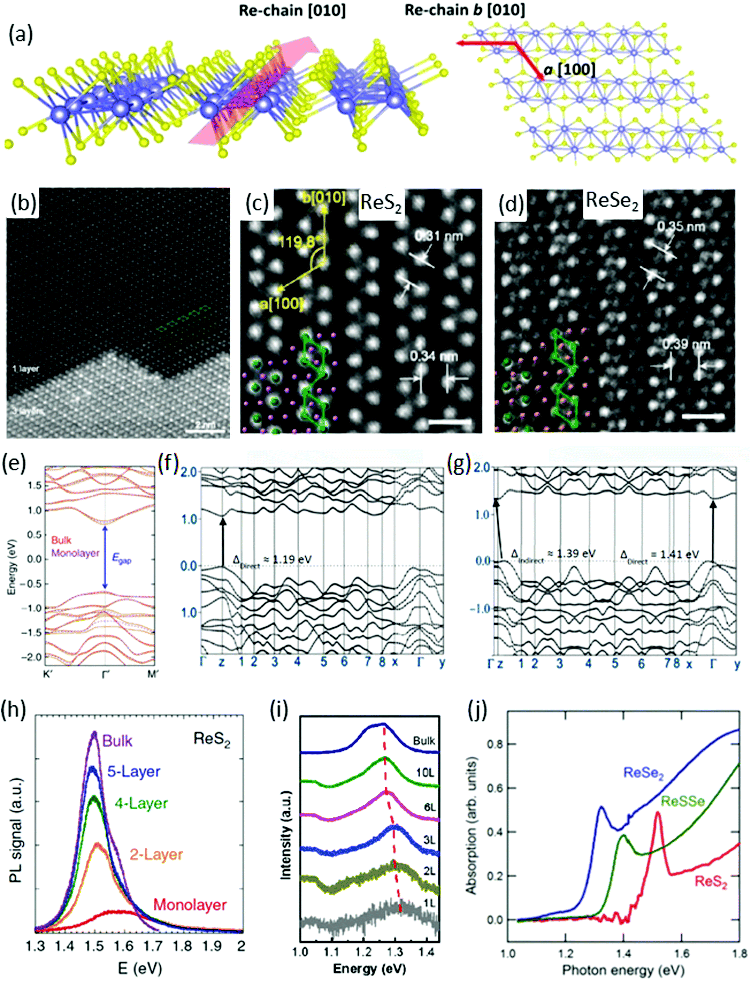 | ||
| Fig. 1 Crystal structure. (a) Schematic depiction of monolayer ReX2 identifying the b-axis [010] Re-chain direction and a-axis [100] across Re-chains. (b) High-magnification ADF image of ReS2. The upper part is single-layer with a diamond-shaped (DS) phase structure, whereas the lower part is three-layer stacking. Four Re atoms form a diamond cluster (green line). The DS clusters form a chain-like structure along the b[010] direction. (c and d) ADF images of ReS2 and ReSe2. The spacing between Re diamond chains is 0.34 and 0.39 nm for ReS2 and ReSe2, respectively. The spacing between Re DS clusters in the chain is 0.31 and 0.35 nm for ReS2 and ReSe2, respectively. Scale bar is 0.5 nm. Reproduced with permission.37 Copyright 2015, American Chemical Society. (e) DFT calculated electronic band structure of bulk (orange solid curves) and monolayer (purple dashed curves) ReS2. Reproduced with permission.26 Copyright 2014, Nature Publishing Group. Both are predicted to be a direct bandgap semiconductor with nearly identical bandgap value at the Gamma point. (f and g) Band structure of monolayer and bulk ReSe2, reproduced with permission.28 Copyright 2014, American Chemical Society. PL spectra of (h) ReS2, reproduced with permission,26 (i) ReSe2, reproduced with permission,25 flakes with different number of layers. (j) Absorption spectrum of ReS2, ReSSe, and ReSe2, reproduced with permission.53 Copyright 2014, Royal Society of Chemistry. | ||
| a (Å) | b (Å) | c (Å) | α (deg) | β (deg) | γ (deg) | |
|---|---|---|---|---|---|---|
| ReS2 | 6.352 | 6.446 | 12.779 | 91.51 | 105.17 | 118.97 |
| ReSe2 | 6.597 | 6.710 | 6.721 | 91.84 | 104.90 | 118.91 |
The direction of the DS Re4 chain is along the b[010] axis (which is also known as the in-plane axis) whereas the a[100] axis (which is known as an out-of-plane axis) and the angle between b[010] and a[100] axes is ∼119.8°, as mentioned in Fig. 1c.26 The spacing between two vicinal diamond-shaped clusters in the direction of b and a is 0.34 and 0.31 nm for ReS2 whereas the spacing is 0.39 and 0.35 nm for ReSe2, respectively, as calculated from ADF images in Fig. 1c and d.37 In the three-layer region in Fig. 1b, the stacking sequence is not 1T, 2H, or 3R, which are well-known for group-VI TMDs.50
The most significant feature of ReS2 is that the bulk and monolayer ReS2 have nearly identical band structures (Fig. 1e). DFT calculations show that the monolayer and bulk form have direct-bandgap and predicted generalized gradient approximation (GGA) bandgaps at 1.35 eV (bulk) and 1.43 eV (monolayer), respectively.26 This nature of band structure is in stark contrast to conventional TMDs, where the band structure is strongly dependent on the number of layers.51 The behaviour of the ReSe2 band structure is quite different and the bandgap is direct in the bulk, and it changes to an indirect bandgap when the layer number decreases to monolayer, as shown in Fig. 1f and g.52 Most importantly, unlike many group-VI TMDs, the indirect gap remains near the K point and the difference between the indirect gap minima and the direct gap is ∼20 meV.46
DFT within GGA and local density approximation (LDA) usually underestimates the bandgap. Photoluminescence (PL) and absorption spectroscopy provide the exact value of bandgap energy and also the effect of thickness on the bandgap of ReS2 and ReSe2. PL measurements were carried out on monolayer, few-layer, and bulk ReS2 (ReSe2) samples and plotted in Fig. 1h (Fig. 1i), respectively. The bandgap for ReS2 was determined to be 1.58 eV (1.5 eV) for monolayer (bulk) samples.22 In the case of ReSe2, owing to the indirect bandgap nature in the monolayer form, the peak intensity is relatively weak for monolayer ReSe2 and increases monotonically when adding layer numbers.
The bandgap increases with deceasing layer numbers, ranging from 1.26 eV for the bulk to 1.32 eV for the monolayer ReSe2 crystals.25 The absorption spectroscopy results of ReS2, ReSSe and ReSe2, are in accordance with PL results.53
Raman spectroscopy is a powerful tool for evaluation of crystal orientations, and identification of the vibration symmetry of chemical bonds.52,54 Recently, it has been used for the determination of layer number in conventional group-VI TMDs such as MoS2 and WS2, where the in-plane and out-of-plane modes show variation in the Raman shift with a variation in the layer number.55,56 However, the situation is completely different for ReX2, where Raman spectra display a similar pattern with the change in thickness of ReX2.42,57–59Fig. 2a and b shows the Raman spectra of N = 1 to N = 7 layers and bulk ReS2 and ReSe2, respectively, recorded at 532 nm laser for randomly oriented samples. Raman measurements from exfoliated ReS2 and ReSe2 flakes display a similar Raman signal regardless of its thickness, as indicated by the data shown in Fig. 2a and b.60 More than 10 modes in the 100–400 cm−1 range can be observed for ReS2 and ReSe2, which is much more than that in TMDs. A large number of Raman peaks is attributed to the low crystal symmetry of ReX2 and associated with fundamental Raman modes (E1g, E2g, and A1g) coupled to each other and to acoustic phonons.26,42 In the case of ReS2, five peaks (151, 161, 213, 238, and 312 cm−1) were assigned to in-plane Eg-like modes, and the peak at 139 cm−1 corresponds to the out-of-plane Ag-like mode.61,62 In the case of ReSe2, the peak at 124 cm−1 was assigned to an in-plane Eg-like mode and the peaks at 162 cm−1 and 174 cm−1 correspond to an out-of-plane Ag-like mode.60
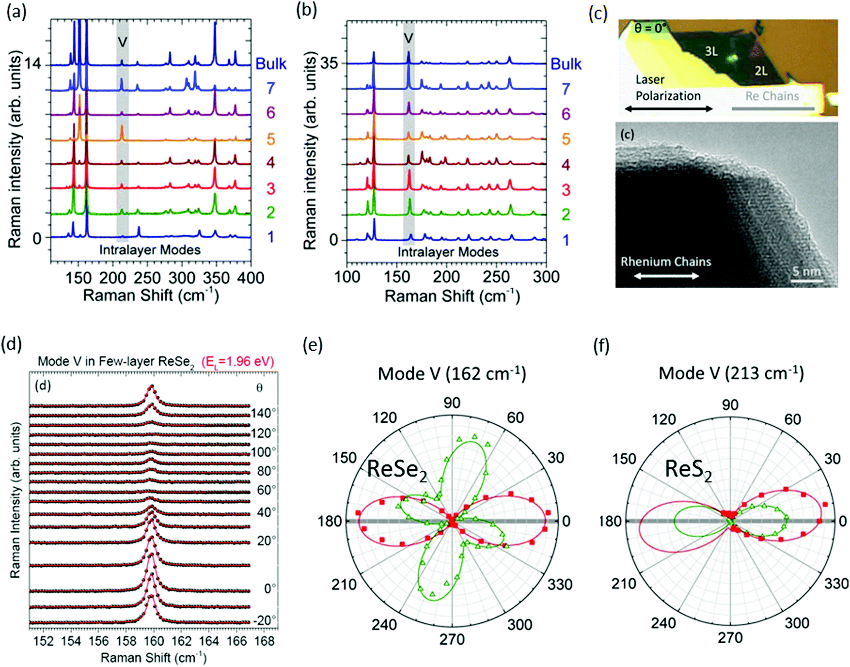 | ||
| Fig. 2 Raman spectra recorded on (a) N-layer ReSe2 and (b) N-layer ReS2 at EL = 2.33 eV in the parallel polarization (XX) configuration; the fifth intralayer mode (V) is highlighted with a gray rectangle. (c) Optical image followed by HRTEM image of the ReSe2 bilayer showing the direction of the Re chains. At θ = 0°, the laser polarization is parallel to the Re chains. (d) Angular dependence of the Raman mode V of ReSe2 recorded as a function of the angle between the linearly polarized laser field and the Re chains in the parallel (XX) polarization configuration. The raw spectra (spheres) are fitted to Voigt profiles (red lines) and are vertically offset for clarity. (e and f) At two photon energies, EL = 1.96 eV (red squares) and EL = 2.33 eV (open green triangles), in the parallel (XX) configuration on the ReSe2 and ReS2 bilayer. The angular patterns are normalized for a clearer comparison. The solid lines fit to the experimental data considering a Raman tensor with complex elements. Reproduced with permission.60 Copyright 2016, American Chemical Society. | ||
Determination of crystal orientation
Raman spectra can also be used to identify the direction of the DS Re4 chain.24,47,52,57,63 For identification of the Re4 direction, only the fifth-lowest frequency mode (denoted as mode V) at ∼162 cm−1 (respectively, 213 cm−1) in ReSe2 (respectively, ReS2) was considered and mentioned in Fig. 2a and b.60 Mainly mode ‘V’ describes the atomic displacement of the Re–Re bond. Three steps are involved in the determination of crystal orientation and direction of the DS Re4 chain. First is an observation: Re chains are found to coincide with one of the cleaved edges of the ReX2 crystals, providing the first hint of the crystal orientation, as can be seen in optical microscope and corresponding high-resolution transmission electron microscopy (HRTEM) images of exfoliated ReSe2 flakes (Fig. 2c). Secondly, the empirical approach that “the integrated intensity of the mode V is maximum when the laser polarization is parallel to the Re chains” was used to confirm the orientation of the ReSe2 chains.Hone and co-workers stated that, at θ = 0°, the laser polarization is parallel to the Re chains, as marked in Fig. 2c.64 Polarization angle-dependent Raman spectroscopy was utilized to study the Raman mode V of ReS2 and ReSe2. Angular dependence of the Raman mode of ReSe2 mode V recorded as a function of the angle between the linearly polarized laser light and the Re chains in the parallel (XX) polarization configuration are shown in Fig. 2d. The third and most important factor is the incoming laser photon energy. These materials efficiently absorb visible light, so the Raman tensor elements are complex numbers. Yang and co-workers predicted a complex manifold of strongly anisotropic excitons in monolayer ReSe2 and ReS2, with several associated optical resonances in the spectral window (1.96–2.33 eV).65 Due to the photon-energy dependence of the anisotropic Raman response in N-layer ReX2, great care must be taken when correlating the angular dependence of the Raman response of an N-layer ReX2 sample to its crystal orientation. Thus, the applicability of this method is valid for ReSe2 while using a 1.96 eV laser, as shown in Fig. 2e. Conversely, it is clear from Fig. 2f that 1.96 eV and 2.33 eV laser lights are acceptable for identification of the DS Re4 chains in ReS2.
Preparation methods and characterizations
Reliable production of large-scale ultrathin 2D ReX2 is essential for further research and applications. In general, two types of approaches (top-down and bottom-up) have been used for preparation of 2D TMDs. Mechanical exfoliation from the bulk is a top-down method and vapor-phase deposition is a bottom-up method. In the following section, we focus on these preparation methods.Conventional Bridgman method
Bhattacharya and co-workers66 employed modified-Bridgman method to grow single crystals of ReS2 and ReSe2 directly from the constituent elements (i.e. pure Re, and S/Se). A 2 cm diameter and 20 cm-long quartz tube was used for the growth, which was cleaned using HF/H2O (1![[thin space (1/6-em)]](https://www.rsc.org/images/entities/char_2009.gif) :10) solution and rinsed thoroughly with distilled water prior to the growth process. This step is crucial because it helps to remove impurities and the etchant also causes a slight roughening to promote nucleation during growth. The constituent elements Re, and S/Se (high purity, ∼5 N) were weighed in stoichiometric proportions individually, introduced into the tube and sealed under vacuum (2 × 10⁻⁶ mbar). Growth was initiated by placing the ampoule into a vertical Bridgman furnace with a specific temperature profile used to obtain single crystals of ReX2 materials. Initially, the temperature was increased to 1100 °C over 72 h. After a stabilization time of 24 h, the temperature was very slowly decreased to 900 °C at 1 °C h−1 over 10 days, after which the tube was cooled down to room temperature at 60 °C h−1. This resulted in the formation of shiny crystals in the form of very thin, plate-like flakes (thickness = hundreds of micrometers; lateral size, approximately 4 × 5 mm2). The optical micrographs and scanning electron microscope (SEM) images of the grown crystals are shown in Fig. 3a–d. High-resolution X-ray diffraction measurements were done to study the structural properties and phase identification of the ReS2 and ReSe2 single crystals, as shown in Fig. 3e and f, respectively. An enlarged view of the most prominent (0 0 l) peak is shown in the inset of Fig. 3e and f. For both samples, only the (0 0 l) reflections were observed, which clearly represent the highly oriented single crystal in the c-axis direction. The sharpness of diffraction peaks, all with full width at half maximum (fwhm) values of <0.1°, clearly indicates the high crystalline quality of the material. Hence, the conventional Bridgman method without utilizing a halogen transport agent can provide high-quality ReX2 crystals. For measurement of layer-dependent properties and device fabrication, thin sheets were used to mechanically exfoliate these flakes and transfer them to SiO2-coated Si substrates for measurements. Another very famous chemical-vapor transport (CVT) method is being widely used to synthesize the bulk of single crystals of ReS2 and ReSe2. The procedure is similar to the method described above using the Bridgman method except that a halogen (I2 or Br2) is used as a transport agent.37,67
:10) solution and rinsed thoroughly with distilled water prior to the growth process. This step is crucial because it helps to remove impurities and the etchant also causes a slight roughening to promote nucleation during growth. The constituent elements Re, and S/Se (high purity, ∼5 N) were weighed in stoichiometric proportions individually, introduced into the tube and sealed under vacuum (2 × 10⁻⁶ mbar). Growth was initiated by placing the ampoule into a vertical Bridgman furnace with a specific temperature profile used to obtain single crystals of ReX2 materials. Initially, the temperature was increased to 1100 °C over 72 h. After a stabilization time of 24 h, the temperature was very slowly decreased to 900 °C at 1 °C h−1 over 10 days, after which the tube was cooled down to room temperature at 60 °C h−1. This resulted in the formation of shiny crystals in the form of very thin, plate-like flakes (thickness = hundreds of micrometers; lateral size, approximately 4 × 5 mm2). The optical micrographs and scanning electron microscope (SEM) images of the grown crystals are shown in Fig. 3a–d. High-resolution X-ray diffraction measurements were done to study the structural properties and phase identification of the ReS2 and ReSe2 single crystals, as shown in Fig. 3e and f, respectively. An enlarged view of the most prominent (0 0 l) peak is shown in the inset of Fig. 3e and f. For both samples, only the (0 0 l) reflections were observed, which clearly represent the highly oriented single crystal in the c-axis direction. The sharpness of diffraction peaks, all with full width at half maximum (fwhm) values of <0.1°, clearly indicates the high crystalline quality of the material. Hence, the conventional Bridgman method without utilizing a halogen transport agent can provide high-quality ReX2 crystals. For measurement of layer-dependent properties and device fabrication, thin sheets were used to mechanically exfoliate these flakes and transfer them to SiO2-coated Si substrates for measurements. Another very famous chemical-vapor transport (CVT) method is being widely used to synthesize the bulk of single crystals of ReS2 and ReSe2. The procedure is similar to the method described above using the Bridgman method except that a halogen (I2 or Br2) is used as a transport agent.37,67
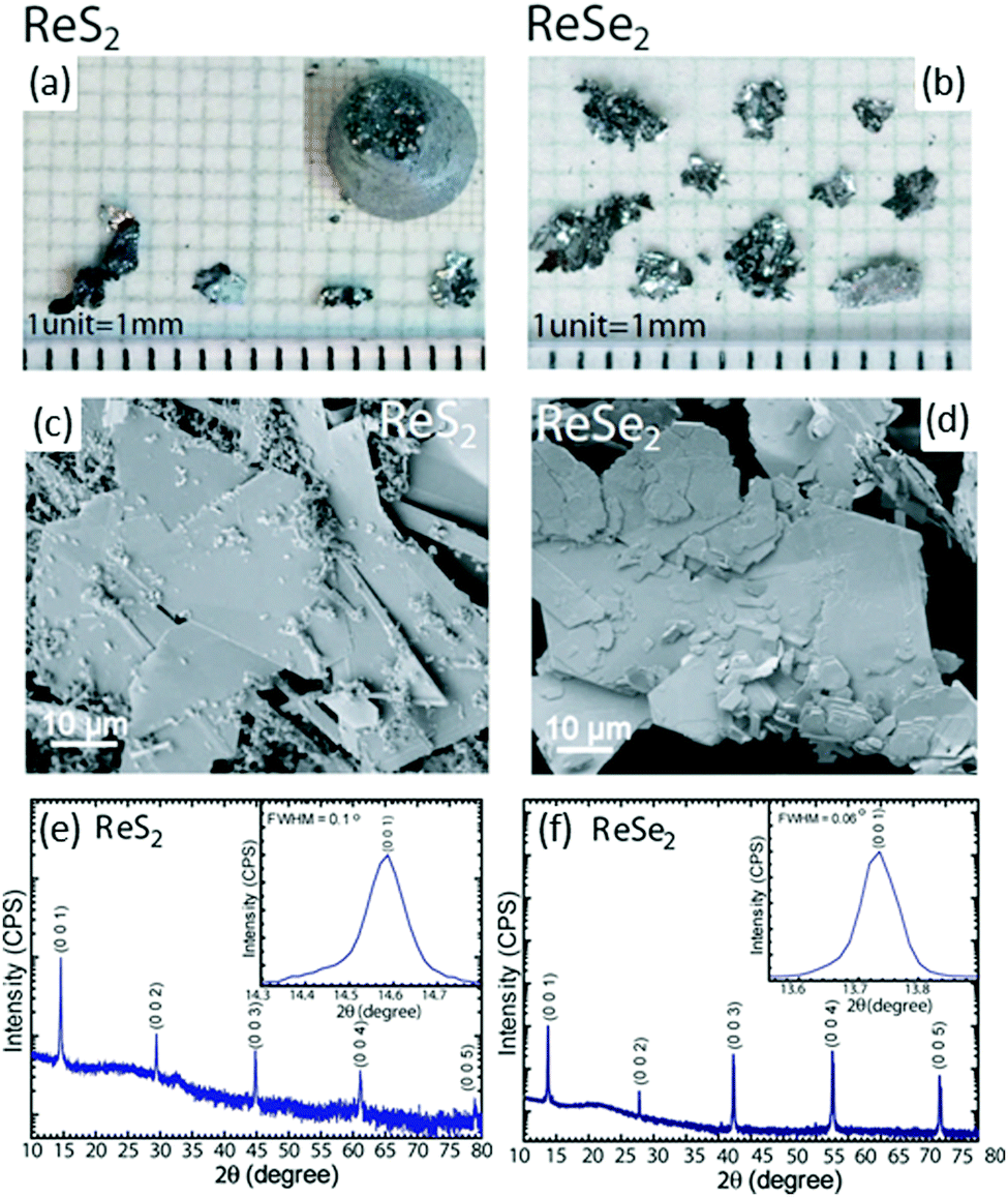 | ||
| Fig. 3 Optical image of the as-grown crystals of (a) ReS2 (inset shows the ingot as removed from the quartz tube) and (b) ReSe2. SEM images of (c) ReS2 and (d) ReSe2, showing the surface morphology of the flakes. HRXRD 2θ scan for (e) ReS2 and (f) ReSe2 single crystals. The patterns were indexed with International Centre for Diffraction Data Powder Diffraction Files 00-052-0818 and 04-007-1113, [2014], for ReS2 and ReSe2, respectively. The y axis is plotted on a log scale. Insets show expanded views of the most prominent reflection. The absence of other (hkl) reflections and the small fwhm values of 0.1 and 0.06° for (0 0 1) reflection of ReS2 and ReSe2, respectively, point to high crystal quality. Reproduced with permission.66 Copyright 2016, American chemical Society. | ||
Physical vapor deposition (PVD)
Zhang and co-workers68 employed a simple thermal-evaporation method to produce a large-area, continuous ReS2 film using ReS2 powder (Alfa-Aesar, 99% purity). ReS2 powder (30 mg) was placed in the middle of quartz tube and SiO2/Si substrate with a 280 nm oxide layer was placed in the downstream, as shown in Fig. 4a. After evacuation of the quartz tube, argon at a flow rate of 50 SCCM was used as the carrier gas. The temperature of the furnace was increased to 900 °C in 60 min and kept at 900 °C for 1 h to grow the ReS2 film and, after the growth, the samples were furnace-cooled to room temperature. Then, the as-grown samples were annealed at 800 °C for 60 min in the argon atmosphere, and then 400 mg of sulfur powder was placed in the upstream at 165 °C. The optical image of as-grown ReS2 film shows a pink (Fig. 4b) continuous ReS2 film of the size of centimeters (Fig. 4c). The pink color indicates that the as-grown film comprises a few layers, and this was confirmed further by atomic force microscopy (AFM) images (Fig. 4d). The height profile shows that the film is homogenous with a thickness of 2.30 nm, which indicates that about three monolayers are present. Furthermore, TEM shows that the thin film is continuous at a nanometer scale (Fig. 4e). Dark-field TEM was employed to observe the grain boundaries, and the average grain size of the as-grown ReS2 film was 250 nm (inset in Fig. 4e). Furthermore, the sharpness of the Raman peaks indicates the good quality of the as-grown ReS2 film, as shown in Fig. 4f.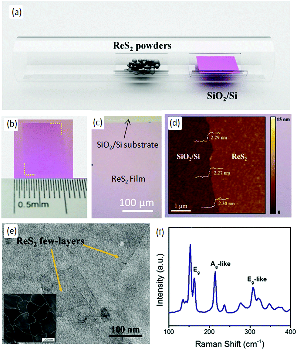 | ||
| Fig. 4 (a) Schematic diagram of synthesized ReS2 film by PVD. Optical (b) photograph and (c) microscope image of grown ReS2 film on the SiO2/Si substrate. (d) is the AFM and (e) TEM image of the ReS2 film. The inset shown in Fig. 3e is the DF-TEM image of ReS2 film. (f) Raman spectrum of ReS2 from 100 cm−1 to 400 cm−1. Reproduced with permission.68 Copyright 2016, Elsevier. | ||
Chemical exfoliation method
Chemical exfoliation from bulk materials is an effective method of TMD production, and lithium intercalation of bulk materials is a well-known exfoliation technique for the scalable production of thin films and composites.69–71 Chen and co workers72 used a solvent-free chemical exfoliated method for the production of ReS2 nanosheets from bulk powders. They used the reaction of ReS2 powder with lithium borohydride (LiBH4) for intercalating Li. This new method could replace the conventional method, which involves a solution of butyl lithium. Lithium intercalation was carried out in a standard oxygen-free, Ar-filled glove box. ReS2 powder (0.1 g) with lithium borohydride (35 mg) were mixed to ensure homogeneity, and then heated to 350 °C for 3 days. The resulting product was immersed in Ar-bubbled water at a ratio of 1 mg per mL of water, and then sonicated for 1 h. Then, lithium cations and non-exfoliated ReS2 were removed by centrifugation. Comparison of the size and shape of the as-received ReS2 powders and as-exfoliated ReS2 nanosheets was carried out by SEM. The grain size of as-received ReS2 powder varied from 100 to 500 nm, whereas the size of as-exfoliated ReS2 nanosheets was reduced to 50–100 nm, as shown in Fig. 5a and b. Optical photographs of a dark-brown homogeneous suspension of chemically exfoliated ReS2 in water is shown in the inset of Fig. 5b. It is clear from the TEM image that the as-exfoliated ReS2 nanosheets were very thin and some were exfoliated down to monolayers, aas confirmed by high-angle annular dark-field STEM (HAADF STEM) image, where the formation of super-lattice DS Re4 chains can be seen easily (Fig. 5c). Raman spectra were taken from as-received powders and as-exfoliated ReS2 nanosheets (Fig. 5d), and significant peak shift or change in phase were not observed. PL spectra (Fig. 5e) were obtained from as-received powders and as-exfoliated ReS2 nanosheets. They revealed that the ReS2 continued to have semiconducting features after exfoliation, which is in the stark contrast to the case of MoS273 and WS2,74 which undergo phase transformation and become metallic.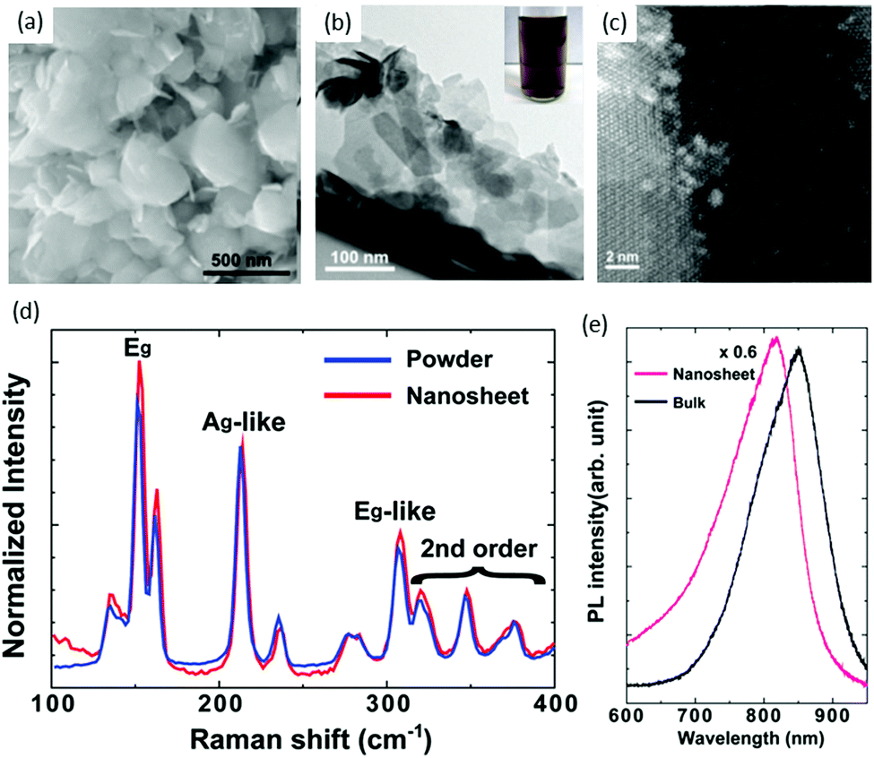 | ||
| Fig. 5 (a) SEM image of as-received ReS2 powders. (b) TEM image of as-exfoliated ReS2 nanosheets; the inset is a photograph of a typical dark-brown exfoliated ReS2 suspension in water. (c) High-resolution STEM image of as-exfoliated ReS2 nanosheets. (d) Raman spectra of as-exfoliated ReS2 nanosheets and as-received powders. (e) PL spectra of as-exfoliated ReS2 nanosheets on an oxidized Si substrate. The spectrum from the bulk (as-received powders) is shown for comparison. Reproduced with permission.72 Copyright 2014, Royal Society of Chemistry. | ||
Chemical vapor deposition (CVD)
The CVD method has been adopted intensively due to the large-area, high-quality and uniform products obtained.17,75,76 The success of achieving large-area CVD-grown graphene77,78 has led the CVD method to be intensively applied to produce large-area, high-quality 2D-layer materials, especially MoS2.5,79 Ajayan and co-workers80 demonstrated the CVD method for the scalable synthesis of large-area monolayer ReS2. They reported a CVD method in which the lowest growth temperature (450 °C) occurs, which is less than all previously CVD-synthesized monolayers (Fig. 6a). Ammonium perrhenate (NH4ReO4) and sulfur powder were used as precursor materials and 280 nm SiO2/Si was used as receiving substrates. NH4ReO4 (0.1 g) was loaded in an alumina boat and SiO2/Si substrates were placed on top of the alumina boat with the polished side facing downwards. The boat was placed in the center of the furnace, as shown in Fig. 6b. Sulfur (2 g) was placed at the opening of the quartz tube furnace. Ar was used as the carrier gas with a flow rate of 50 sccm. The furnace was ramped to 450 °C in 15 min (sulfur temperature was ∼300 °C) and then held at 450 °C for 20 min with a constant Ar flow rate under atmospheric pressure. Then, the samples were furnace-cooled to 35 °C. SEM was employed for the surface analysis. As-grown ReS2 samples and SEM images revealed the growth of thin and clean ReS2 crystals with different sizes and hexagonal shapes, as shown in Fig. 6c. The size of the crystals varied from 2 to 60 μm, with a mean size of 40 μm.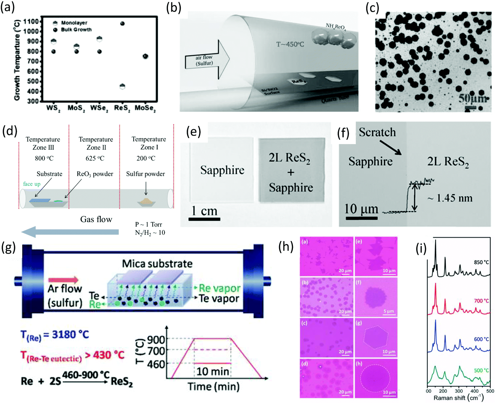 | ||
| Fig. 6 (a) Growth temperatures for various CVD grown monolayers and for bulk crystal growth of various TMDs along with temperatures for ReS2. (b) Schematic for the CVD growth of monolayer ReS2. (c) SEM image showing various ReS2 monolayer crystals. Reproduced with permission.80 Copyright 2015, Wiley-VCH. (d) Schematic for the hydrogen-assisted large-area CVD growth approach. (e) A picture of bare and as-grown ReS2 bilayer (2L) film on sapphire wafer. (f) Optical microscope image of the ReS2 bilayer film grown on sapphire substrates; a scratch was made intentionally for clarity, and the inset shows the height profile. Reproduced with permission.62 Copyright 2016, Wiley-VCH. (g) Schematic for the tellurium-assisted CVD growth approach. Temperature-dependent growth behavior of ReS2. (h) OM images of ReS2 grown at 850, 700, 600, and 500 °C after transfer to a SiO2/Si substrate. Followed by enlarged images. (i) Raman spectra of ReS2 grown at different temperatures. Reproduced with permission.87 Copyright 2016, Wiley-VCH. | ||
After the first report of the CVD growth of ReS2, many attempts were made with mixed success to increase the quality and maintenance of the shape and large-area growth.47,59,79,81,82 Zhai and co-worker62 employed a hydrogen-assisted CVD method for the synthesis of large-area uniform polycrystalline ReS2 film and hexagonal single-crystal ReS2 flakes. Similar to the conventional method of TMDs growth in which MoO383 was used to synthesize MoS2,79,84 MoSe285 and WO3 for the growth of WS286 and WSe2,35 ReO3 (10 mg) and S (3 g) were used as precursor materials for the growth of ReS2. The synthesis of bilayers ReS2 was carried out in a quartz tube using a three-zone horizontal tube furnace. In brief, sapphires pieces (2 cm × 2 cm) were placed in the tube furnace onto an alumina boat containing precursor material (ReO3), as shown in Fig. 6d. Growth of large-area ReS2 bilayers was carried out at low pressure (∼1 Torr) and a carrier gas of high purity (N2 and H2) was used at 800 °C for 10 min. After the growth, the samples were furnace-cooled to room temperature. After the growth, an obvious dark membrane could be observed compared with the bare substrate, as shown in Fig. 6e. An AFM height profile was employed to measure the thickness, and found to be ∼1.45 nm from the edge of a scratch (Fig. 6f). A highly uniform large-growth area was observed only for the sapphire substrate, which might be attributed to the weak van der Waals interaction between ReS2 and sapphire.
Zhang and co-workers87 introduced a new (tellurium-assisted) CVD method to reduce the melting point of the precursor material, and achieved high-quality monolayer ReS2 at a large scale on mica substrate. The actual melting temperature of Re metal is 3180 °C and the eutectic point of Re–Te binary alloy is very low (down to 850 °C) and can be 430 °C if the Te–Re weight ratio is ≤90%. The whole synthetic process is illustrated in Fig. 6g. Briefly, Re and Te powders were mixed together and the weight ratio kept at 1:6. These mixed powders were loaded into a ceramic boat, and freshly cleaved mica substrates were put on the ceramic boat. Then, the boat was placed in the center of quartz tube. The boat (which contained sulfur powder) was placed near the outside edge of the hot zone. Ar was used as a carrier gas at a constant flow rate of 80 sccm, growth temperatures of 460–900 °C and growth time of 10 min, as described in Fig. 6g. Furthermore, the sharpness of Raman spectra indicated that high-quality ReS2 could be obtained above 600 °C (Fig. 6i). This shows that the growth temperature has an important role in the crystal quality and morphological control of ReS2 (Fig. 6h and i).
Zhai and co-workers88 used a CVD method for the first time to synthesize ReSe2 flakes and continuous film. The existence of pure H2 gas in the carrier gas and the ratio of N2 to H2 was the key to synthesize high-quality ReSe2. High-purity ReO3 and Se powders were used as precursor materials and SiO2/Si wafers with a 280 nm SiO2 layer as substrates. Several SiO2/Si (2 cm × 2 cm) and sapphire pieces were placed on an alumina boat containing precursor material (ReO3) and the boat was loaded in the middle of a tube furnace, as shown in Fig. 7a. Se (1 g) was placed in the low-temperature zone at 200 °C and high purity N2 and H2 was used as a carrier gas, as shown in Fig. 7a. Then, the furnace was heated to 625 °C in 15 min and stayed at a maximum temperature for 10 min. After the growth, the samples were furnace-cooled to room temperature. As-synthesized samples were characterized by optical microscopy and the final product was hexagonal-shaped ReSe2 flakes with lateral size up to 5 μm (Fig. 7b). A slight variation was observed between different ReSe2 flakes, as can be seen from the color variation in the magnified image in the inset of Fig. 7b. The thickness of ReSe2 flakes was further investigated by height profile using AFM. The measured height was ∼4.2 nm, which corresponded to six layers of ReSe2 (Fig. 7c). Interestingly, a wrinkle feature was observed in thin ReSe2 flakes, which is common in metal selenides such as WSe289 and Bi2Se3.90 Raman signals of ReSe2 hexagonal flakes displayed a similar Raman signal, which is in accordance with reported work.60 The sharpness of Raman modes clearly indicates the high crystalline quality of as-synthesized ReSe2 flakes. Sample composition was evaluated by energy dispersive X-ray spectroscopy (EDX) and an atomic ratio of 33.03 Re to 66.97 Se was deduced from the EDX spectrum, which matched well with the stoichiometric ratio of ReSe2. All these characterizations indicated that as-grown ReSe2 flakes were of high-quality crystal.
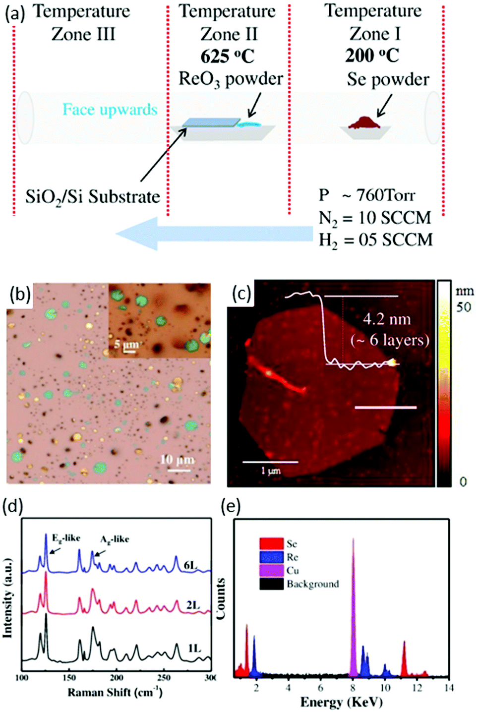 | ||
| Fig. 7 CVD synthesis of ReSe2, (a) schematic the CVD growth approach, (b) optical microscope (OM) image of the ReSe2 hexagonal flakes grown on SiO2/Si substrates; inset shows the magnified OM image for the clarity. (c) AFM image of the corresponding ReSe2 hexagons and the inset shows the AFM height profile for the ReSe2 hexagon. (d) Raman spectra collected from different thicknesses of the as-synthesized ReSe2 hexagons. (e) EDX spectrum of the ReSe2 flake. Reproduced with permission.88 Copyright 2016, Wiley-VCH. | ||
Device applications
Due to weak interlayer coupling, ReS2 remains a direct band-gap material upon reduction of the thickness from bulk to monolayer. This implies that thicker samples of ReS2 could have a higher density of states and enhanced light absorption. Therefore, few-layer ReS2 becomes an ideal candidate for highly responsive photodetectors.Photodetectors based on ReX2
Xiu and co-workers82 fabricated two-terminal back-gate photodetectors based on CVD-grown few-layers of ReS2, as shown in Fig. 8a. The device was probed using a focused laser beam (633 nm) with laser power ranging from 12.5 to 1000 nW, with a continuous 50 V back gate bias (Fig. 8b). A significant increase of the photocurrent was observed and showed a strong dependence on gate bias and laser power. Maximum photoresponsivity was measured up to 16.14 A W−1 and the external quantum efficiency reached to 3168%. Time-resolved photo-detection exhibited a stable and repeatable response, but the response was very slow (∼104 s) with a small on/off ratio of ≈2.8 (Fig. 8c), as compared with photodetectors based on conventional TMDs. This slow photo-response may be due to poor morphologies and ambiguous, trailing electron diffraction spots of synthesized ReS2.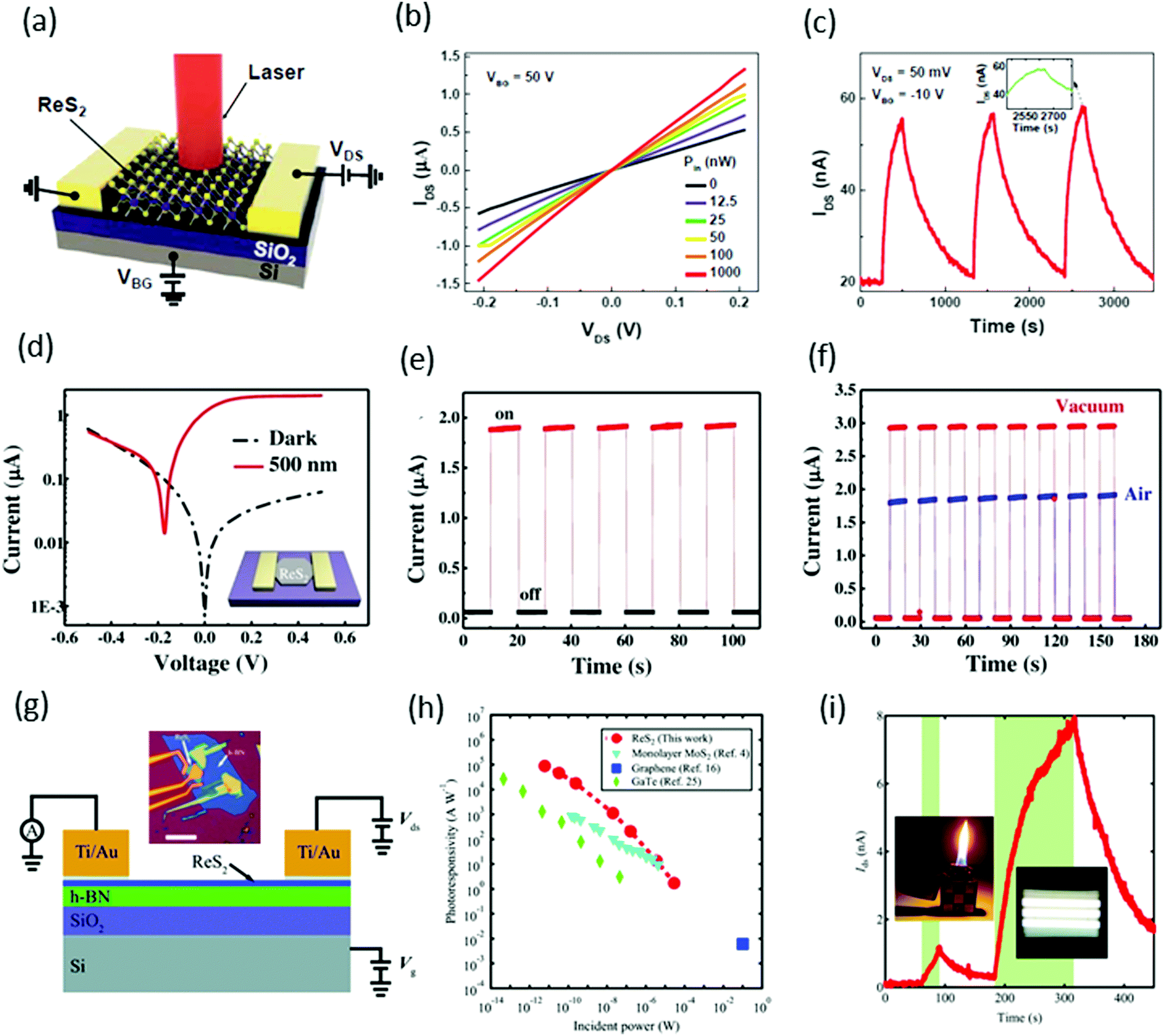 | ||
| Fig. 8 (a) Schematic structure of a ReS2 photodetector device. (b) IV characteristics of the device under different incident laser power Pin. (c) Time-dependent IDS of the device with and without laser illumination. Inset, plot of the photoresponse peak over a small range, which shows a tendency toward saturation. Reproduced with permission.82 Copyright 2015, Wiley-VCH. (d) The characteristic current–voltage (I–V) curve of the single ReS2 hexagon device fabricated on a freshly cleaned SiO2/Si substrate; inset shows the schematic image of the device. (e) The stable and repetitive switching characteristic curves with the light (500 nm) turned on/off periodically at 10 s intervals with a bias of 0.5 V. (f) Time-dependent photo-response curves in different environments (air and vacuum). Reproduced with permission.83 Copyright 2016, Wiley-VCH. (g) Schematic and measurement circuit of few-layer ReS2 phototransistors. (h) Optical microscopy image of a few-layer ReS2 phototransistor. The scale bar is 10 μm. (i) The dependence of RP on light. Under weak illumination (≈6 pW), RP reached ≤88600 A W−1. For comparison, the results from monolayer MoS2, multilayer GaTe, and graphene are also presented. The error bar is smaller than the size of the dots. Weak signal detection in a 5-layer ReS2 phototransistor using a lighter and limited fluorescent lighting as the weak light sources. Vbg was fixed at −50 V and Vds was fixed at 2.0 V. The areas with light-green background represent the states under illumination. Reproduced with permission.92 Copyright 2016, Wiley-VCH. | ||
Zhai and co-workers62 fabricated photodetector devices based on high-quality CVD-grown single-crystal hexagonal ReS2 flakes. A 500 nm incident light of power intensity 3.11 mW cm−2 was illuminated perpendicularly to the devices. The measured photocurrent was 1.85 μA with an on–off ratio ≈32 and an ultrafast response time of 2 ms, as shown in Fig. 8e. The calculated responsivity of ReS2 hexagons was ≈604 A W−1 with an EQE ≈ 1.50 × 10⁵% and a specific detectivity D* ≈ 4.44 × 10¹⁰ Jones. Moreover, the photocurrent in a vacuum was larger than that in air, which revealed the n-type nature of as-grown ReS2 flakes (Fig. 8f). The high performance of the photodetector was attributed to the Schottky contact, high quality of samples, and the weak interlayer coupling in ReS2.
Xing and co-worker91 introduced a new method for the fabrication of photodetector devices. They used a buffer layer between the few-layer ReS2 and SiO2/Si substrate, as shown in Fig. 8g. The h-BN layer was helpful to reduce the scattering from impurities in the substrate, as has been shown to improve the device performance in graphene92 and MoS2.93 The devices were illuminated under 532 nm laser light with power ranging from 6 pW to 29 μW, under the fixed bias of 4.0 V and a back gate voltage fixed at −50 V. Under the minimum power 6 pW, the measured photoresponsivity of the ReS2 phototransistor reached ≤88 600 A W−1 and the external quantum efficiency reached 2 × 10⁷%. These values are the highest values among the reported photodetectors based on 2D materials, monolayer MoS2,94 multilayer GaTe95 and graphene96 (Fig. 8h). Due to the ultra-high sensitivity of few-layer ReS2 phototransistors, they are suitable for the detection of very weak signals such as lighter (photocurrent ∼1 nA) and fluorescent lighting (photocurrent ∼7.6 nA), as shown in Fig. 8i.
In the case of ReSe2, the presence of Re4 chains makes it an optically biaxial material that shows exceptionally anisotropic electrical and optical behavior for linearly polarized light. Wei and co-workers45 reported the first monolayer ReSe2-based photodetector. The monolayers were exfoliated from a bulk sample and vacuum-annealed to remove remaining residue. Devices were fabricated by standard e-beam lithography with 5 nm-thick Cr and 50 nm-thick gold contacts, whereas the width (W) and length (L) of the channel in the device were both ∼2 μm, as shown in the schematic and AFM image (inset) in Fig. 9a. A 633 nm laser with optical power intensity of 100 mW cm−2 was focused onto the devices, and time-dependent photo-responses were measured in various gas environments. The photo-responsivity (in air) was calculated to be 17.8 A W−1 and external quantum efficiency (EQE) was 3484%. These values are quite good and reasonable compared with other conventional TMDs.
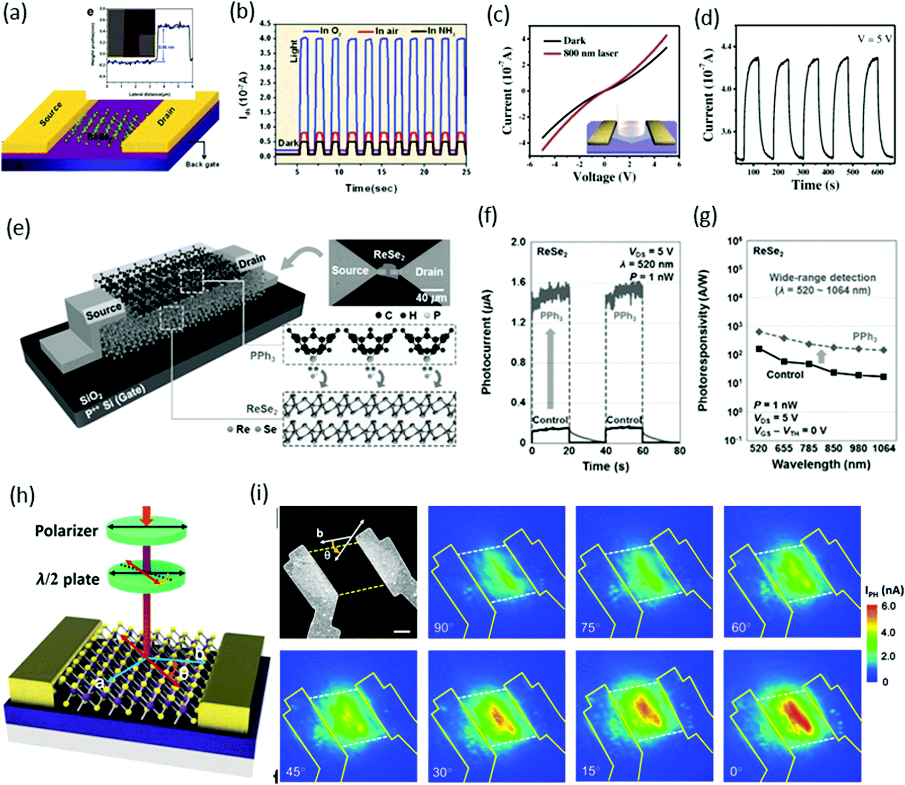 | ||
| Fig. 9 (a) A schematic of a single-layer ReSe2 FET together with two gold electrodes. Inset: Atomic force microscopy (AFM) image of the device based on the ReSe2 single layer. (b) Time-dependent photoresponse with bias voltage Vds = 0.5 V in O2, air or NH3 environment with light (633 nm, 100 mW cm−2). Reproduced with permission.45 Copyright 2014, Royal Society of Chemistry. (c) Characteristic current–voltage (I–V) curve of the single ReSe2 hexagon device fabricated on a SiO2/Si substrate; inset shows a schematic image of the device. (d) The stable and repetitive switching characteristic curves with the light (808 nm) turned on/off periodically at 60 s intervals with a bias of 5 V. Reproduced with permission.88 Copyright 2016, Wiley-VCH. (e) Schematic diagram and optical image of back-gated (90 nm thick SiO2 gate dielectric) ReSe2 devices doped by PPh3 and a descriptive illustration for the n-doping mechanism by PPh3 at the PPh3/ReSe2 interface. Reproduced with permission.97 Copyright 2016, Wiley-VCH. (f) Photoresponse as a function of time obtained before and after PPh3 doping. (g) Photoresponsivity of ReSe2 photodetectors as a function of the wavelength. (h) Schematic structure of polarization-sensitive photodetectors based on ReSe2 nanosheets. (i) SEM image of the ReSe2 photodetector followed by polarization-dependent photocurrent mapping of the device, showing prominent linear dichroic photodetection. The thickness of the ReSe2 channel is 12 nm. Reproduced with permission.98 Copyright 2016, American Chemical Society. | ||
Zhai and coworkers88 fabricated photodetector devices by using same device structure employed by Wei et al. but with CVD-grown ReSe2 hexagonal flakes, as shown schematically in Fig. 9c. A significant change in the current (∼100 nA) was observed under a 808 nm incident light of power intensity 566 mW cm−2, as shown in Fig. 9c. The photodetector devices were very stable and completely reversible, as shown in a cyclability test (Fig. 9d). The photo-responsivity was calculated to be ∼2.98 A W−1 and maximum EQE was 4.58 × 10²%. These values are comparable with an earlier report of exfoliated samples.
Park and co-workers97 introduced a new method for the enhancement of photoresponses by improving the source-side contact resistance through a triphenyl phosphine (PPh3)-based n-doping technique, as shown schematically in Fig. 9e. The temporal photoresponse was measured in the undoped (control) and PPh3-doped ReSe2 photodetectors by using 520 nm laser light with 1 nW laser power, as presented in Fig. 9f. By performing the PPh3-based n-doping process, a significant enhancement from 3.97 × 10³ A W−1 to 3.68 × 10⁴ A W−1 was observed. Fig. 9g reveals that a broad range of photo-detection (possible above 1064 nm) can be achieved with ultrafast photo-switching (τr = 30 ms and τd = 64 ms).
Xiu and co-workers98 reported polarization-sensitive photodetection behavior due to the intrinsic linear dichroism originating from high in-plane optical anisotropy. Usually, linear dichroism requires an anisotropic crystal and Raman spectroscopy reveals high in-plane crystal anisotropy in ReSe2. A light polarizer and a half-wave plate were used to change the angle θ between the polarization direction of incident laser (633 nm) and the b-axis (DS chains direction) of the sample, as shown in Fig. 9h. Fig. 9i shows that the photocurrent has a maximum value when the incident light is polarized along the b crystal axis (0° polarization) and reaches a minimum at the perpendicular setup (90° polarization).
FET based on ReX2
FET is one of the most elementary components in electronics, and consists of three parts: (i) drain–source metal contacts, (ii) dielectric layer (gate electrode), and (iii) semiconducting channel. The drain–source current is controlled by the gate voltage on the dielectric layer. Xing and co-workers61 reported the performance of back-gated FET devices based on the different thicknesses of ReS2 channels. Fig. 10a shows the FET transfer curve (for monolayer and trilayers) obtained by measuring the source–drain current Ids while sweeping the back-gate voltage Vbg from −50 to +50 V with a fixed 100 mV source–drain bias voltage Vsd. The inset of Fig. 10a presents the optical image of a typical monolayer device. Both devices behaved as excellent n-type semiconductors with an excellent current on/off ratio of ∼107, which indicates that ReS2 is a suitable material for many applications in electronics. Subthreshold swing can also be measured from the transfer curves, and was measured as 310 mV per decade for a monolayer device and 100 mV per decade for the trilayer device, as shown in Fig. 10a. These values are comparable with top-gated MoS2 transistors99 and outperform black-phosphorus100 devices. The layer number (monolayer to 7 layers)-dependent properties of FET devices were studied and plotted in Fig. 10c. The mobility of monolayer device varied between 0.1 and 2.6 cm2 V−1 s−1, and the highest mobility was obtained as 15.4 cm2 V−1 s−1 for a six-layer device. This difference in mobility values with the same number of layers could be induced by the anisotropic property. Suenaga and coworkers37 investigated the relationship between the atomic structure and anisotropic transport properties. ReS2 flakes were exfoliated onto SiO2/Si and the number of layers was identified using color contrast in the optical microscope, as shown in Fig. 10d. Electrodes were deposited opposite to each other and marked as 1, 2, 3, and 4 (Fig. 10d). Electrical measurements were carried out and plotted in Fig. 10e. The high-magnification ADF image of the ReS2 device shows Re diamond chains to be aligned parallel to the 1–4 and 2–3 direction. The two-terminal conductance parallel to the b-axis was 0.82 μS for Vds = 1 V and Vg = 20 V, whereas conductance perpendicular to the b axis was one order of magnitude smaller (0.075 μS). The mobility of the device along the b-axis was calculated to be μ1–4 = 23.1 cm2 (V s)−1, whereas electrons exhibited lower mobility (14.8 cm2 (V s)−1) perpendicular to the b-axis (Fig. 10f).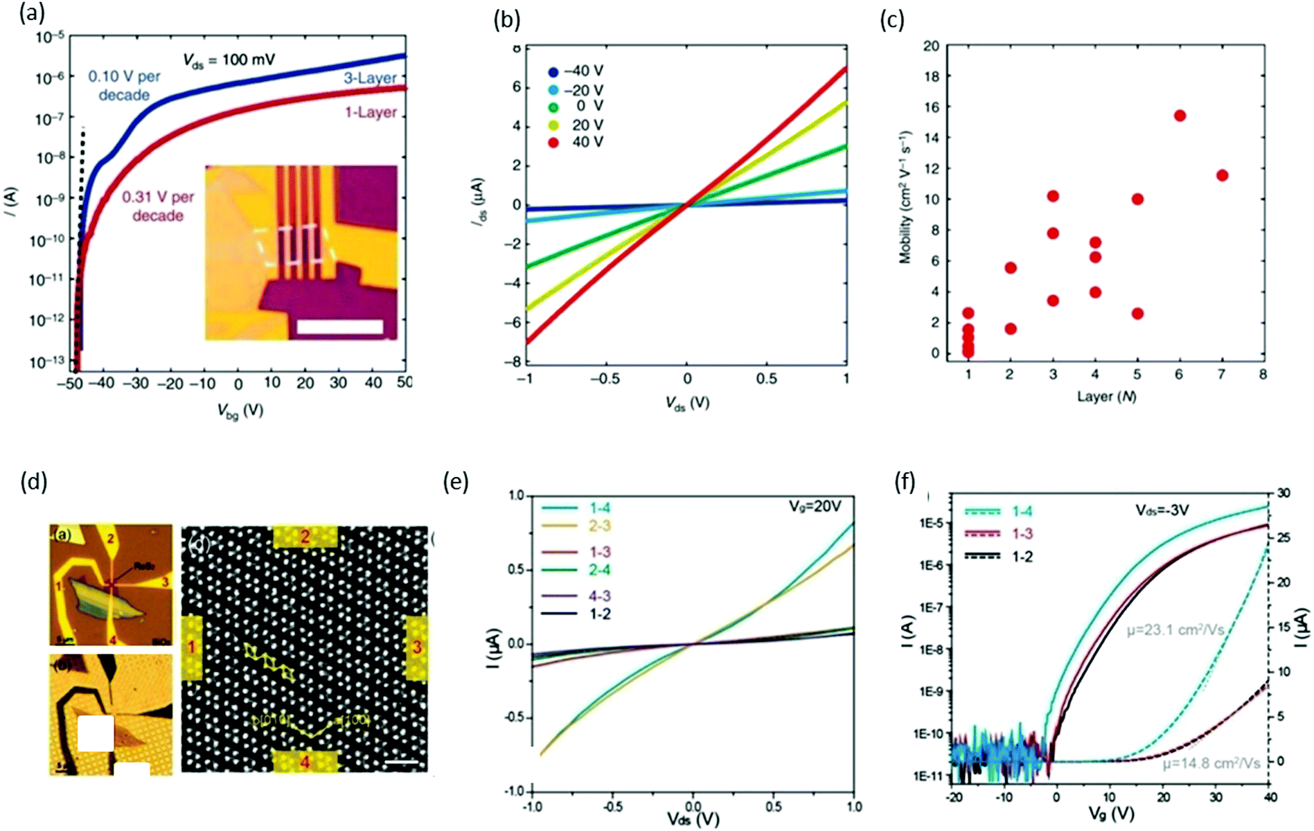 | ||
| Fig. 10 ReS2 field-effect transistor devices. (a) Transfer curves of monolayer (red) and trilayer (blue) ReS2 FET devices. Vds is fixed at 100 mV. The on/off ratio is ∼107 for the monolayer device and 107 for the seven-layer device. The subthreshold swings are 310 mV per decade (monolayer) and 100 mV per decade (trilayer), respectively. Inset: Optical image of a typical monolayer ReS2 FET device. Scale bar, 5 mm. (b) Ids–Vds curves of a monolayer ReS2 FET at different Vbg, with linear dependence indicating ohmic contact. (c) The dependence of device mobility on the number of layers. In general, the mobility increases monotonically with the number of layers with some scattering. Reproduced with permission.61 Copyright 2015, Nature Publishing Group. (d) Optical microscope image of a ReS2 four-probe transistor on a SiO2/Si substrate. Channel length and width of the device between the opposite contacts, e.g., 1–3 and 2–4, are 1 and 0.3 μm. The approximate channel length and width for adjacent contacts, e.g., 1–2, 2–3, 3–4, and 1–4, are 0.7 and 0.3 μm. (b) Back-lighting optical microscopic image of the identical ReS2 device transferred onto a TEM quantifoil. The magnified ADF images taken are at a scale bar of 1 nm. (e) The direction-dependent I–V characteristics with applied back gate voltage Vg = 20 V. (f) The direction-dependent transfer characteristics with drain–source bias of −3 V. Reproduced with permission.36 Copyright 2015, American Chemical Society. | ||
The intrinsic transport properties of ReSe2 were studied and showed ambipolar behaviour:98 two types of a four-terminal back-gate ReSe2 FETs devices were fabricated on, SiO2 (285 nm)/Si or hBN/SiO2 (7/285 nm). Fig. 11(a) and (d) display a schematic device structure of two kinds of devices; correspondingly, the optical images are provided in the insets of Fig. 11b and e. A four-probe configuration was used for the conductance measurement to avoid contact resistance, and hBN and SiO2 served as the gate dielectric. Parts b and e of Fig. 11 display the temperature-dependent conductance as a function of VBG of the devices built on SiO2 and hBN/SiO2 substrates, respectively. Both devices exhibited ambipolar behavior and the temperature-dependent electron and hole mobilities are plotted in Fig. 11c and f. The ReSe2 devices on hBN/SiO2 exhibited a significant increase in electron motility over 500 (3) times and hole mobility over 100 (60) times at low (room) temperature. This improvement in mobility from the devices on hBN/SiO2 can be attributed to less scattering from charged impurities.
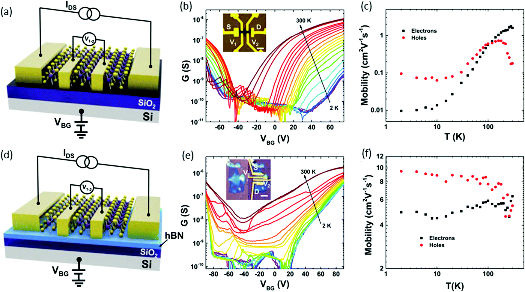 | ||
| Fig. 11 Temperature-dependent transport properties of four-terminal few-layer ReSe2 FETs on SiO2 and hBN substrates. (a) Schematic structure of a ReSe2 back-gate FET on a SiO2 substrate. (b) Temperature-dependent sheet conductance versus back-gate voltage showing evident ambipolar behavior of the device on a SiO2 (285 nm) substrate. The channel is 6 nm thick. Inset: Optical image of the FET device. Scale bar, 5 μm. (c) Extracted four-terminal field-effect electron and hole mobility versus temperature for the device on a SiO2 substrate. (d) Schematic structure of the device on a hBN/SiO2 substrate. (e) Temperature-dependent sheet conductance versus back-gate voltage of the device on a hBN/SiO2 (7 nm/285 nm) substrate with a channel thickness of 7 nm. Inset: Optical image of the sample before and after the electrode fabrication. Scale bar, 4 μm. (f) Extracted four-terminal field-effect electron and hole mobility versus temperature for the device on a hBN/SiO2 substrate. Reproduced with permission.98 Copyright 2016, American Chemical Society. | ||
Prospects for thermoelectric applications
The 2D structure and low symmetry-induced anisotropy have affected the thermoelectric performance significantly, as reported recently for the case of black phosphorus,101 SnSe102 and TaX2 (X = S, Se).103 Hence, these unique anisotropic ReX2 materials may also be useful for enhancing the thermoelectric performance. Unlike other 2D materials, these ReX2 have weak interlayer coupling, and the electronic free carriers may have to transport across the van der Waals interface through a tunneling effect whereas the phonon transport will go through van der Waals interfaces. Thus, the ratio between these two types of transport may be different from the usually strong interlayer coupling interfaces, which may result in an enhancement of the thermoelectric figure of merit (ZT).Conclusions
In this review, we have made a concise and comprehensive summary of the typical fundamental properties and potential applications of a new member, ReX2 (X = S, Se), in the 2D TMDs family. Compared with other methods, vapor deposition is considered to be the most successful method for high-quality ReX2 fabrication. Crystal orientation-dependent photodetector and FETs measurements revealed that the performance has a strong positive relationship with the b-axis direction. Raman spectroscopy can be a powerful tool for the determination of crystal orientation, which paves the way for future applications in the anisotropic properties of ReX2. With regard to synthesis, future research is expected to focus on large-area high-quality ReX2 film or pattern growth of ReX2 single crystals, which are the basic requirements for integrated circuits. For study of devices, (opto-)electronic properties combined with the anisotropic features of ReX2 could be a hot topic. Finally, the recent exciting achievements on the study of 2D ReX2 have opened up new opportunities for further research on 2D TMDs.Acknowledgements
This work was supported by the National Natural Science Foundation of China (91622117, 51472097, and 21501060), National Key Research and Development Program of “Strategic Advanced Electronic Materials” (2016YFB0401100), National Basic Research Program of China (2015CB932600), Program or HUST Interdisciplinary Innovation Team (2015ZDTD038) and the Fundamental Research Funds for the Central University. The authors are indebted for the kind permission from the corresponding publishers/authors to reproduce their materials (especially figures) in this review article.Notes and references
- L. Gan, X. Ou, Q. Zhang, R. Wu and Z. Luo, Chem. Mater., 2014, 26, 4137–4143 CrossRef CAS.
- I. Meric, M. Y. Han, A. F. Young, B. Ozyilmaz, P. Kim and K. L. Shepard, Nat. Nanotechnol., 2008, 3, 654–659 CrossRef CAS PubMed.
- G. Heo, Y. S. Kim, S.-H. Chun and M.-J. Seong, Nanoscale Res. Lett., 2015, 10, 45 CrossRef PubMed.
- X. Huang, Z. Zeng and H. Zhang, Chem. Soc. Rev., 2013, 42, 1934–1946 RSC.
- Y. Shi, H. Li and L.-J. Li, Chem. Soc. Rev., 2015, 44, 2744–2756 RSC.
- H. P. Komsa, J. Kotakoski, S. Kurasch, O. Lehtinen, U. Kaiser and A. V. Krasheninnikov, Phys. Rev. Lett., 2012, 109, 1–5 CrossRef PubMed.
- X. Zhou, Q. Zhang, L. Gan, H. Q. Li and T. Y. Zhai, Adv. Funct. Mater., 2016, 26, 4405–4413 CrossRef CAS.
- L. Li, W. K. Wang, L. Gan, N. Zhou, X. D. Zhu, Q. Zhang, H. Q. Li, M. L. Tian and T. Y. Zhai, Adv. Funct. Mater., 2016, 26, 8281–8289 CrossRef CAS.
- X. Zhou, Q. Zhang, L. Gan, H. Li, J. Xiong and T. Y. Zhai, Adv. Sci., 2016, 3, 1600177 CrossRef PubMed.
- Y. Ma, Sci. Bull., 2015, 60, 1789–1790 CrossRef.
- C. Ataca, H. Şahin and S. Ciraci, J. Phys. Chem. C, 2012, 116, 8983–8999 CAS.
- R. Pan, X. L. Fan, H. Zhang and Y. Yang, Comput. Mater. Sci., 2016, 122, 118–125 CrossRef CAS.
- R. Ganatra and Q. Zhang, ACS Nano, 2014, 8, 4074–4099 CrossRef CAS PubMed.
- C. M. Corbet, C. McClellan, A. Rai, S. S. Sonde, E. Tutuc and S. K. Banerjee, ACS Nano, 2015, 9, 363–370 CrossRef CAS PubMed.
- H. Wang, H. Yuan, S. Sae Hong, Y. Li and Y. Cui, Chem. Soc. Rev., 2015, 44, 2664–2680 RSC.
- Y. F. Lin, Y. Xu, S. T. Wang, S. L. Li, M. Yamamoto, A. Aparecido-Ferreira, W. Li, H. Sun, S. Nakaharai, W. Bin Jian, K. Ueno and K. Tsukagoshi, Adv. Mater., 2014, 26, 3263–3269 CrossRef CAS PubMed.
- X. Zhou, L. Gan, W. Tian, Q. Zhang, S. Jin, H. Li, Y. Bando, D. Golberg and T. Zhai, Adv. Mater., 2015, 22, 8035–8041 CrossRef PubMed.
- S. Yang, Y. Li, X. Wang, N. Huo, J.-B. Xia, S.-S. Li and J. Li, Nanoscale, 2014, 6, 2582–2587 RSC.
- P. Hu, Z. Wen, L. Wang, P. Tan and K. Xiao, ACS Nano, 2012, 6, 5988–5994 CrossRef CAS PubMed.
- P. Hu, L. Wang, M. Yoon, J. Zhang, W. Feng, X. Wang, Z. Wen, J. C. Idrobo, Y. Miyamoto, D. B. Geohegan and K. Xiao, Nano Lett., 2013, 13, 1649–1654 CrossRef CAS PubMed.
- H. Fang, S. Chuang, T. C. Chang, K. Takei, T. Takahashi and A. Javey, Nano Lett., 2012, 12, 3788–3792 CrossRef CAS PubMed.
- Z. Yin, H. Li, H. Li, L. Jiang, Y. Shi, Y. Sun, G. Lu, Q. Zhang, X. Chen and H. Zhang, ACS Nano, 2012, 6, 74–80 CrossRef CAS PubMed.
- Y. Yu, C. Li, Y. Liu, L. Su, Y. Zhang and L. Cao, Sci. Rep., 2013, 3, 1866 Search PubMed.
- S. Yang, C. Wang, H. Sahin, H. Chen, Y. Li, S. S. Li, A. Suslu, F. M. Peeters, Q. Liu, J. Li and S. Tongay, Nano Lett., 2015, 15, 1660–1666 CrossRef CAS PubMed.
- J. A. Wilson and A. D. Yoffe, Adv. Phys., 1969, 18, 193–335 CrossRef CAS.
- S. Tongay, H. Sahin, C. Ko, A. Luce, W. Fan, K. Liu, J. Zhou, Y.-S. Huang, C.-H. Ho, J. Yan, D. F. Ogletree, S. Aloni, J. Ji, S. Li, J. Li, F. M. Peeters and J. Wu, Nat. Commun., 2014, 5, 3252 Search PubMed.
- C. Ho, Cryst. Struct. Theory Appl., 2013, 2, 65–69 Search PubMed.
- D. Wolverson, S. Crampin, A. S. Kazemi, A. Ilie and S. J. Bending, ACS Nano, 2014, 8, 11154–11164 CrossRef CAS PubMed.
- H.-J. Lamfers, A. Meetsma, G. A. Wiegers and J. L. de Boer, J. Alloys Compd., 1996, 241, 34–39 CrossRef CAS.
- P. Mirõ, M. Ghorbani-Asl and T. Heine, Angew. Chem., Int. Ed., 2014, 53, 3015–3018 CrossRef PubMed.
- Z. Xu, Y. Zhang, S. Lin, C. Zheng, Y. L. Zhong, X. Xia, Z. Li, P. J. Sophia, M. S. Fuhrer, Y. Cheng and Q. Bao, ACS Nano, 2015, 9, 6178–6187 CrossRef CAS PubMed.
- Y. Chen, L. Gan, H. Q. Li, Y. Ma and T. Y. Zhai, Adv. Mater., 2017, 29, 1603550 CrossRef PubMed.
- J. Xia, X. Huang, L. Z. Liu, M. Wang, L. Wang, B. Huang, D. D. Zhu, J. J. Li, C. Z. Gu and X. M. Meng, Nanoscale, 2014, 6, 8949–8955 RSC.
- A. Abderrahmane, P. J. Ko, T. V. Thu, S. Ishizawa, T. Takamura and A. Sandhu, Nanotechnology, 2014, 25, 365202 CrossRef CAS PubMed.
- J. Chen, B. Liu, Y. Liu, W. Tang, C. T. Nai, L. Li, J. Zheng, L. Gao, Y. Zheng, H. S. Shin, H. Y. Jeong and K. P. Loh, Adv. Mater., 2015, 27, 6722–6727 CrossRef CAS PubMed.
- Y. You, X.-X. Zhang, T. C. Berkelbach, M. S. Hybertsen, D. R. Reichman and T. F. Heinz, Nat. Phys., 2015, 11, 477–481 CrossRef CAS.
- Y. C. Lin, H. P. Komsa, C. H. Yeh, T. Björkman, Z. Y. Liang, C. H. Ho, Y. S. Huang, P. W. Chiu, A. V. Krasheninnikov and K. Suenaga, ACS Nano, 2015, 9, 11249–11257 CrossRef CAS PubMed.
- K. K. Tiong, C. H. Ho and Y. S. Huang, Solid State Commun., 1999, 111, 635–640 CrossRef CAS.
- Y. C. Lin, H. P. Komsa, C. H. Yeh, T. Bjorkman, Z. Y. Liang, C. H. Ho, Y. S. Huang, P. W. Chiu, A. V. Krasheninnikov and K. Suenaga, ACS Nano, 2015, 9, 11249–11257 CrossRef CAS PubMed.
- D. Hou, Y. Ma, J. Du, J. Yan, C. Ji and H. Zhu, J. Phys. Chem. Solids, 2010, 71, 1571–1575 CrossRef CAS.
- A. Taube, A. Lapinska, J. Judek and M. Zdrojek, Appl. Phys. Lett., 2015, 107, 13105 CrossRef.
- Y. Feng, W. Zhou, Y. Wang, J. Zhou, E. Liu, Y. Fu, Z. Ni, X. Wu, H. Yuan, F. Miao, B. Wang, X. Wan and D. Xing, Phys. Rev. B: Condens. Matter Mater. Phys., 2015, 92, 1–6 Search PubMed.
- Y. Yu, S. Y. Huang, Y. Li, S. N. Steinmann, W. Yang and L. Cao, Nano Lett., 2014, 14, 553–558 CrossRef CAS PubMed.
- S. Walia, S. Balendhran, Y. Wang, R. Ab Kadir, A. Sabirin Zoolfakar, P. Atkin, J. Zhen Ou, S. Sriram, K. Kalantar-Zadeh and M. Bhaskaran, Appl. Phys. Lett., 2013, 103, 232105 CrossRef.
- Y. Zhang, Y. Zhang, Q. Ji, J. Ju, H. Yuan, J. Shi, T. Gao, D. Ma, M. Liu, Y. Chen, X. Song, H. Y. Hwang, Y. Cui and Z. Liu, ACS Nano, 2013, 7, 8963–8971 CrossRef CAS PubMed.
- S. Yang, S. Tongay, Y. Li, Q. Yue, J.-B. Xia, S.-S. Li, J. Li and S.-H. Wei, Nanoscale, 2014, 6, 7226–7231 RSC.
- K. Wu, B. Chen, S. Yang, G. Wang, W. Kong, H. Cai, T. Aoki, E. Soignard, X. Marie, A. Yano, A. Suslu, B. Urbaszek and S. Tongay, Nano Lett., 2016, 16, 5888–5894 CrossRef CAS PubMed.
- H. Murray, S. Kelty, R. Chianelli and C. Day, Inorg. Chem., 1994, 33, 4418–4420 CrossRef CAS.
- C. M. Fang, G. A. Wiegers, C. Haas and R. A. de Groot, J. Phys.: Condens. Matter, 1997, 9, 4411–4424 CrossRef CAS.
- D. Voiry, A. Mohite and M. Chhowalla, Chem. Soc. Rev., 2015, 44, 2702–2712 RSC.
- S. Tongay, W. Fan, J. Kang, J. Park, U. Koldemir, J. Suh, D. S. Narang, K. Liu, J. Ji, J. Li, R. Sinclair and J. Wu, Nano Lett., 2014, 14, 3185–3190 CrossRef CAS PubMed.
- L. Hart, S. Dale, S. Hoye, J. L. Webb and D. Wolverson, Nano Lett., 2016, 16, 1381–1386 CrossRef CAS PubMed.
- F. Liu, S. Zheng, A. Chaturvedi, V. Zólyomi, J. Zhou, Q. Fu, C. Zhu, P. Yu, Q. Zeng, N. D. Drummond, H. J. Fan, C. Kloc, V. I. Fal’ko, X. He and Z. Liu, Nanoscale, 2016, 8, 5826–5834 RSC.
- X. Wang, A. M. Jones, K. L. Seyler, V. Tran, Y. Jia, H. Zhao, H. Wang, L. Yang, X. Xu and F. Xia, Nat. Nanotechnol., 2015, 10, 517–521 CrossRef CAS PubMed.
- K. K. Liu, W. Zhang, Y. H. Lee, Y. C. Lin, M. T. Chang, C. Y. Su, C. S. Chang, H. Li, Y. Shi, H. Zhang, C. S. Lai and L. J. Li, Nano Lett., 2012, 12, 1538–1544 CrossRef CAS PubMed.
- W. Zhao, Z. Ghorannevis, K. K. Amara, J. R. Pang, M. Toh, X. Zhang, C. Kloc, P. H. Tan and G. Eda, Nanoscale, 2013, 5, 9677–9683 RSC.
- P. Nagler, G. Plechinger, C. Schüller and T. Korn, Phys. Status Solidi RRL, 2016, 10, 185–189 CrossRef CAS.
- O. B. Aslan, D. A. Chenet, A. M. van der Zande, J. C. Hone and T. F. Heinz, ACS Photonics, 2016, 3, 96–101 CrossRef CAS.
- Q. Zhang, S. Tan, R. G. Mendes, Z. Sun, Y. Chen, X. Kong, Y. Xue, M. H. Rümmeli, X. Wu, S. Chen and L. Fu, Adv. Mater., 2016, 28, 2616–2623 CrossRef CAS PubMed.
- E. Lorchat, G. Froehlicher and S. Berciaud, ACS Nano, 2016, 10, 2752–2760 CrossRef CAS PubMed.
- E. Liu, Y. Fu, Y. Wang, Y. Feng, H. Liu, X. Wan, W. Zhou, B. Wang, L. Shao, C.-H. Ho, Y.-S. Huang, Z. Cao, L. Wang, A. Li, J. Zeng, F. Song, X. Wang, Y. Shi, H. Yuan, H. Y. Hwang, Y. Cui, F. Miao and D. Xing, Nat. Commun., 2015, 6, 6991 CrossRef CAS PubMed.
- M. Hafeez, L. Gan, H. Li, Y. Ma and T. Zhai, Adv. Funct. Mater., 2016, 24, 4551–4560 CrossRef.
- Q. Zhang, W. Wang, X. Kong, R. G. Mendes, L. Fang, Y. Xue, Y. Xiao, M. H. Rümmeli, S. Chen and L. Fu, J. Am. Chem. Soc., 2016, 138, 11101–11104 CrossRef CAS PubMed.
- D. A. Chenet, O. B. Aslan, P. Y. Huang, C. Fan, A. M. van der Zande, T. F. Heinz and J. C. Hone, Nano Lett., 2015, 15, 5667–5672 CrossRef CAS PubMed.
- H. X. Zhong, S. Gao, J. J. Shi and L. Yang, Phys. Rev. B: Condens. Matter Mater. Phys., 2015, 92, 1–7 CrossRef.
- B. Jariwala, D. Voiry, A. Jindal, B. A. Chalke, R. Bapat, A. Thamizhavel, M. Chhowalla, M. Deshmukh and A. Bhattacharya, Chem. Mater., 2016, 28, 3352–3359 CrossRef CAS.
- Z. Yin, H. Li, H. Li, L. Jiang, Y. Shi, Y. Sun, G. Lu, Q. Zhang, X. Chen and H. Zhang, ACS Nano, 2012, 6, 74–80 CrossRef CAS PubMed.
- F. Qi, Y. Chen, B. Zheng, J. Zhou, X. Wang, P. Li and W. Zhang, Mater. Lett., 2016, 184, 324–327 CrossRef CAS.
- V. Nicolosi, M. Chhowalla, M. G. Kanatzidis, M. S. Strano and J. N. Coleman, Science, 2013, 340, 1226419 CrossRef.
- J. N. Coleman, M. Lotya, A. O’Neill, S. D. Bergin, P. J. King, U. Khan, K. Young, A. Gaucher, S. De, R. J. Smith, I. V. Shvets, S. K. Arora, G. Stanton, H.-Y. Kim, K. Lee, G. T. Kim, G. S. Duesberg, T. Hallam, J. J. Boland, J. J. Wang, J. F. Donegan, J. C. Grunlan, G. Moriarty, A. Shmeliov, R. J. Nicholls, J. M. Perkins, E. M. Grieveson, K. Theuwissen, D. W. McComb, P. D. Nellist and V. Nicolosi, Science, 2011, 331, 568–571 CrossRef CAS PubMed.
- J. Zheng, H. Zhang, S. Dong, Y. Liu, C. T. Nai, H. S. Shin, H. Y. Jeong, B. Liu and K. P. Loh, Nat. Commun., 2014, 5, 2995 Search PubMed.
- T. Fujita, Y. Ito, Y. Tan, H. Yamaguchi, D. Hojo, A. Hirata, D. Voiry, M. Chhowalla and M. Chen, Nanoscale, 2014, 6, 12458–12462 RSC.
- D. Voiry, M. Salehi, R. Silva, T. Fujita, M. Chen, T. Asefa, V. B. Shenoy, G. Eda and M. Chhowalla, Nano Lett., 2013, 13, 6222–6227 CrossRef CAS PubMed.
- D. Voiry, H. Yamaguchi, J. Li, R. Silva, D. C. B. Alves, T. Fujita, M. Chen, T. Asefa, V. B. Shenoy, G. Eda and M. Chhowalla, Nat. Mater., 2013, 12, 850–855 CrossRef CAS PubMed.
- Y. H. Lee, X. Q. Zhang, W. Zhang, M. T. Chang, C. Te Lin, K. Di Chang, Y. C. Yu, J. T. W. Wang, C. S. Chang, L. J. Li and T. W. Lin, Adv. Mater., 2012, 24, 2320–2325 CrossRef CAS PubMed.
- L. Chen, B. Liu, M. Ge, Y. Ma, A. N. Abbas and C. Zhou, ACS Nano, 2015, 9, 8368–8375 CrossRef CAS PubMed.
- Y. Wu, Y. Lin, A. A. Bol, K. A. Jenkins, F. Xia, D. B. Farmer, Y. Zhu and P. Avouris, Nature, 2011, 472, 74–78 CrossRef CAS PubMed.
- S. Karamat, S. Sonuşen, Ü. Çelik, Y. Uysallı, E. Özgönül and A. Oral, Prog. Nat. Sci.: Mater. Int., 2015, 25, 291–299 CrossRef CAS.
- S. S. Wang, Y. M. Rong, Y. Fan, M. Pacios, H. Bhaskaran, K. He and J. H. Warner, Chem. Mater., 2014, 26, 6371–6379 CrossRef CAS.
- K. Keyshar, Y. Gong, G. Ye, G. Brunetto, W. Zhou, D. P. Cole, K. Hackenberg, Y. He, L. Machado, M. Kabbani, A. H. C. Hart, B. Li, D. S. Galvao, A. George, R. Vajtai, C. S. Tiwary and P. M. Ajayan, Adv. Mater., 2015, 27, 4640–4648 CrossRef CAS PubMed.
- X. He, F. Liu, P. Hu, W. Fu, X. Wang, Q. Zeng, W. Zhao and Z. Liu, Small, 2015, 11, 5423–5429 CrossRef CAS PubMed.
- E. Zhang, Y. Jin, X. Yuan, W. Wang, C. Zhang, L. Tang, S. Liu, P. Zhou, W. Hu and F. Xiu, Adv. Funct. Mater., 2015, 16, 4076–4082 CrossRef.
- Y. C. Lin, W. Zhang, J. K. Huang, K. K. Liu, Y. H. Lee, C. T. Liang, C. W. Chud and L. J. Li, Nanoscale, 2012, 4, 6637–6641 RSC.
- Y. Kim, H. Bark, G. H. Ryu, Z. Lee and C. Lee, J. Phys.: Condens. Matter, 2016, 28, 6 Search PubMed.
- X. Wang, Y. Gong, G. Shi, W. L. Chow, K. Keyshar, G. Ye, R. Vajtai, J. Lou, Z. Liu, E. Ringe, B. K. Tay and P. M. Ajayan, ACS Nano, 2014, 8, 5125–5131 CrossRef CAS PubMed.
- A. Thangaraja, S. M. Shinde, G. Kalita and M. Tanemura, Mater. Lett., 2015, 156, 156–160 CrossRef CAS.
- F. Cui, C. Wang, X. Li, G. Wang, K. Liu, Z. Yang, Q. Feng, X. Liang, Z. Zhang, S. Liu, Z. Lei, Z. Liu, H. Xu and J. Zhang, Adv. Mater., 2016, 28, 5019–5024 CrossRef CAS PubMed.
- M. Hafeez, L. Gan, H. Li, Y. Ma and T. Zhai, Adv. Mater., 2016, 28, 8296–8301 CrossRef CAS PubMed.
- L. Chen, B. Liu, A. N. Abbas, Y. Ma, X. Fang, Y. Liu and C. Zhou, ACS Nano, 2014, 8, 11543–11551 CrossRef CAS PubMed.
- A. Zhuang, J. J. Li, Y. C. Wang, X. Wen, Y. Lin, B. Xiang, X. Wang and J. Zeng, Angew. Chem., Int. Ed., 2014, 53, 6425–6429 CrossRef CAS PubMed.
- E. Liu, M. Long, J. Zeng, W. Luo, Y. Wang, Y. Pan, W. Zhou, B. Wang, W. Hu, Z. Ni, Y. You, X. Zhang, S. Qin, Y. Shi, K. Watanabe, T. Taniguchi, H. Yuan, H. Y. Hwang, Y. Cui, F. Miao and D. Xing, Adv. Funct. Mater., 2016, 26, 1938–1944 CrossRef CAS.
- C. R. Dean, A. F. Young, I. Meric, C. Lee, L. Wang, S. Sorgenfrei, K. Watanabe, T. Taniguchi, P. Kim, K. L. Shepard and J. Hone, Nat. Nanotechnol., 2010, 5, 722–726 CrossRef CAS PubMed.
- X. Cui, G.-H. Lee, Y. D. Kim, G. Arefe, P. Y. Huang, C. Lee, D. A. Chenet, X. Zhang, L. Wang, F. Ye, F. Pizzocchero, B. S. Jessen, K. Watanabe, T. Taniguchi, D. A. Muller, T. Low, P. Kim and J. Hone, Nat. Nanotechnol., 2015, 10, 534–540 CrossRef CAS PubMed.
- O. Lopez-Sanchez, D. Lembke, M. Kayci, A. Radenovic and A. Kis, Nat. Nanotechnol., 2013, 8, 497–501 CrossRef CAS PubMed.
- F. Liu, H. Shimotani, H. Shang, T. Kanagasekaran, V. Zólyomi, N. Drummond, V. I. Fal’Ko and K. Tanigaki, ACS Nano, 2014, 8, 752–760 CrossRef CAS PubMed.
- T. Mueller, F. Xia and P. Avouris, Nat. Photonics, 2010, 4, 297–301 CrossRef CAS.
- S. H. Jo, H. Y. Park, D. H. Kang, J. Shim, J. Jeon, S. Choi, M. Kim, Y. Park, J. Lee, Y. J. Song, S. Lee and J. H. Park, Adv. Mater., 2016, 28, 6711–6718 CrossRef CAS PubMed.
- E. Zhang, P. Wang, Z. Li, H. Wang, C. Song, C. Huang, Z. G. Chen, L. Yang, K. Zhang, S. Lu, W. Wang, S. Liu, H. Fang, X. Zhou, H. Yan, J. Zou, X. Wan, P. Zhou, W. Hu and F. Xiu, ACS Nano, 2016, 10, 8067–8077 CrossRef CAS PubMed.
- B. Radisavljevic, A. Radenovic, J. Brivio, V. Giacometti and A. Kis, Nat. Nanotechnol., 2011, 6, 147–150 CrossRef CAS PubMed.
- L. Li, Y. Yu, G. J. Ye, Q. Ge, X. Ou, H. Wu, D. Feng, X. H. Chen and Y. Zhang, Nat. Nanotechnol., 2014, 9, 372–377 CrossRef CAS PubMed.
- H. H. Fu, D. D. Wu, L. Gu, M. Wu and R. Wu, Phys. Rev. B: Condens. Matter Mater. Phys., 2015, 92, 045418 CrossRef.
- L. D. Zhao, S. H. Lo, Y. Zhang, H. Sun, G. Tan, C. Uher, C. Wolverton, V. P. Dravid and M. G. Kanatzidis, Nature, 2014, 508, 373–377 CrossRef CAS PubMed.
- M. Souheyr, F. Houda, O. Tarik and E. Claude, J. Alloys Compd., 2013, 581, 731–740 CrossRef.
| This journal is © the Partner Organisations 2017 |