
Ultrathin few layer oxychalcogenide BiCuSeO nanosheets†‡
Manisha
Samanta
,
Satya N.
Guin
and
Kanishka
Biswas
*
New Chemistry Unit, Jawaharlal Nehru Centre for Advanced Scientific Research (JNCASR), Jakkur P.O., Bangalore 560064, India. E-mail: kanishka@jncasr.ac.in
First published on 1st November 2016
Abstract
Layered materials with intrinsically low thermal conductivity are promising candidates for thermoelectric waste heat to electrical energy conversion. Recently bulk form BiCuSeO, a layered oxychalcogenide, has drawn attention for thermoelectric applications. However, synthesis of a two dimensional nanosheet of BiCuSeO and study of its thermoelectric properties have not been explored yet. Here, we present a facile surfactant free low temperature solvothermal synthesis of few layered ultrathin BiCuSeO nanosheets for the first time. Nanosheets of BiCuSeO exhibit a semiconducting band gap of 0.9 eV and p-type conduction. A dense hot pressed pellet of BiCuSeO nanosheets exhibits a superior power factor and lower lattice thermal conductivity compared to that of the bulk sample in the temperature range of 300–723 K.
Introduction
Inorganic solids with layered structures are one of the major untapped sources of two dimensional (2D) materials, which can produce new 2D nanosheets with exotic properties. The graphene boom motivated researchers to search for new non-carbon based ultrathin 2D inorganic solids.1–8 The high surface to volume ratio and quantum confinement effect of charge carriers in two dimensions result in various interesting properties and applications such as electronic devices, catalysis, energy storage and energy conversion.1–8Thermoelectric materials will play a pivotal role in future energy management by harvesting waste heat and converting it into electrical energy.9–11 Narrow band gap semiconducting inorganic solids are important materials for thermoelectric applications.9–11 Anisotropic materials with layered structures such as Bi2Te3, Sb2Te3 and Bi2Se3 have been enormously explored for thermoelectric applications.12–14 The anisotropic crystal structure and bonding result in substantial differences in the thermoelectric properties in different crystallographic directions. For example, SnSe, which is a layered narrow band gap semiconductor, exhibits ultralow thermal conductivity with a record high zT ∼ 2.6 along the crystallographic b axis.15–17
Layered quaternary metal oxychalcogenides, MCuXO (M = La, Ce, Nd, Pr, Bi, and In; X = Te, Se and S) have been found to be important materials for thermoelectrics, superconductivity and interesting electronic transport.18,19 The presence of covalent metal–chalcogen and ionic metal–oxygen units in the layered structure leads to unique structural chemistry and exciting properties. Preferential bonding of chalocogen and oxygen with one particular type of cation results in low dimensional structures in MCuXO, which leads to anisotropic electronic structures and properties.
BiCuSeO is an interesting material from the oxychalcogenide family and has recently gained attention for thermoelectric applications due to its low thermal conductivity.20 BiCuSeO is a multiband semiconductor and crystallizes in a ZrCuSiAs type layered structure with a tetragonal unit cell (space group P4/nmm).18–22 The crystal structure of BiCuSeO consists of insulating (Bi2O2)2+ and conductive (Cu2Se2)2− layers, which are stacked along the crystallographic c axis of the tetragonal cell (Fig. 1a). The (Bi2O2)2+ layers consist of distorted Bi4O tetrahedra (fluorite type structure), whereas (Cu2Se2)2− layers consist of distorted CuSe4 tetrahedra (anti-fluorite type structure).20,21 The phonon–phonon Umklapp processes originate from the scattering of phonons from the interface due to the layered structure, soft bonding and lattice anharmonicity, which result in low thermal conductivity in BiCuSeO.20 The thermoelectric properties of bulk BiCuSeO have been improved by a carrier engineering strategy using metal ion (e.g. Mg2+, Ca2+, Sr2+ and Ba2+) doping or introducing single and dual vacancies.21,23–27
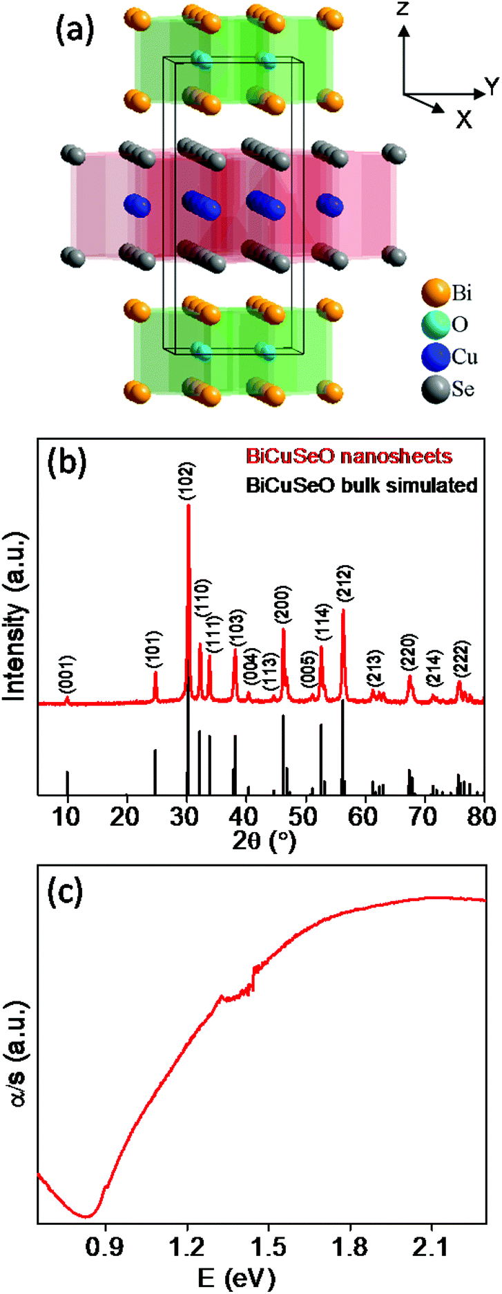 | ||
| Fig. 1 (a) Crystal structure of BiCuSeO demonstrating the layered structure.19 (b) Powder XRD patterns of as synthesized BiCuSeO nanosheets. (c) Optical absorption spectrum of as synthesized BiCuSeO nanosheets. | ||
A bottom-up wet chemical synthesis of inorganic solids in the form of 2D nanosheets/nanoplates is an effective strategy for tuning the thermoelectric properties of bulk layered materials.14,28,29 The ultrathin 2D form of layered materials can lead to the quantum confinement of carriers, which can cause an enhancement in the Seebeck coefficient. Effective phonon scattering from the interfaces of nanosheets may result in reduction of lattice thermal conductivity. The free standing single layered Bi2Se3 showed excellent thermoelectric properties compared to that of its bulk counterpart due to improved electronic transport and reduced thermal conductivity.28–31 Kinetically synthesized few layered nanosheets of intergrowth (MX)m(E2X3)n [where M = Pb; E = Bi; X = Te, Se] homologous compounds exhibit ultra-low thermal conductivity due to phonon scattering by the heterostructure interface.32,33 Recently, ultrathin nanosheets of SnSe and SnSe2 were synthesized by soft chemical synthesis, and showed a high power factor and low thermal conductivity.34,35 This motivated us to synthesize and study the thermoelectric properties of pristine BiCuSeO nanosheets.
Herein, we demonstrate a low temperature surfactant-free soft chemical synthesis of ultrathin (∼4–5 layers and 3–4 nm thick) BiCuSeO nanosheets for the first time. Large scale few layered BiCuSeO nanosheets were synthesized by the reaction of Bi(NO3)2·5H2O, Cu(NO3)2·3H2O and selenourea in the presence of KOH/NaOH under solvothermal conditions. Transmission electron microscopy (TEM) and atomic force microscopy (AFM) characterizations indicate the 2D nanosheet morphology of the sample. Room temperature optical absorption studies indicate that as-synthesized BiCuSeO nanosheets exhibit a band gap of ∼0.9 eV. A significantly low lattice thermal conductivity in the range of 0.55–0.4 W m−1 K−1 was measured in a hot pressed dense pellet of BiCuSeO nanosheets in the 300–700 K range, which is lower than that of the bulk BiCuSeO. Extensive phonon scattering from the interfaces of the layers, bond anharmonicity and nanoscale grain boundaries resulted in low thermal conductivity in BiCuSeO nanosheets. Undoped BiCuSeO nanosheets exhibit p-type conduction (carrier concentration ∼3.8 × 1018 cm−3) and a higher average power factor value than that of the bulk sample.
Experimental section
Chemicals
Bismuth nitrate – Bi(NO3)3·5H2O (Alfa Aesar, 99.9%), selenourea – SeC(NH2)2 (Alfa Aesar, 99%), copper nitrate – Cu(NO3)2·3H2O (Alfa Aesar, 99%), potassium hydroxide – KOH, sodium hydroxide – NaOH and ethanol were used without further purification.Synthesis of BiCuSeO nanosheets
In order to synthesize BiCuSeO nanosheets, 100 mg of Bi(NO3)2·5H2O (0.206 mmol) is dissolved in a mixture of 5 ml water and 5 ml ethanol upon stirring, which resulted in a milky white solution. To the resulting solution, 25.4 mg of selenourea (0.206 mmol) is added with stirring, which produced an orange colour. Finally, 120 mg of KOH, 320 mg of NaOH and 49.8 mg of Cu(NO3)2·3H2O (0.206 mmol) are subsequently added with continuous stirring. The resulting black solution is then transferred into a 50 ml Teflon lined stainless steel autoclave and kept in a hot air oven at 180 °C for 1 day. The obtained as synthesized black coloured product is then washed 3 times with distilled water and ethanol and the purified product is then dried under ambient conditions.Powder X-ray diffraction
Room temperature powder X-Ray diffraction of all the samples was carried out in a Rigaku diffractometer using Cu-Kα radiation (λ = 1.5406 Å). Data were collected in the 2θ range of 20° to 80° with a step of 1° per minute.Band gap measurement
In order to probe the optical band gap of the powder sample, diffuse reflectance spectroscopy was carried out using a Perkin Elmer Lambda 900, UV/VIS/NIR spectrometer in reflectance mode. Absorption (α/S) data were estimated from reflectance data using the Kubelka–Munk equation: α/S = (1 − R)2/2R, where R is reflectance and α and S are the absorption and scattering co-efficient, respectively. The energy band gap was obtained from a α/S (a.u.) vs. Eg (eV) plot.Field emission scanning electron microscopy (FESEM)
For FESEM imaging, a NOVA NANO SEM 600 (FEI, Germany) instrument, operated at 15 kV, was used and energy dispersive spectroscopy (EDAX) analysis was performed with an EDAX Genesis instrument attached to the FESEM column. A drop of BiCuSeO nanosheets dispersed in toluene was placed on a silicon substrate and dried for FESEM imaging.Transmission electron microscopy (TEM)
The TEM experiment was performed using a JEOL (JEM3010) TEM operating at a 300 kV accelerating voltage fitted with a Gatan CCD camera. Along with this, additional TEM images were taken using a FEI TECNAI G2 20 STWIN TEM operating at 200 kV and elemental mapping was performed in STEM imaging mode. For sample preparation for TEM imaging, one drop of BiCuSeO nanosheets dispersed in toluene was drop casted on a holey carbon coated Cu grid.X-ray photoelectron spectroscopy (XPS)
An Omicron Nanotechnology spectrometer with an Mg-Kα (1253.6 eV) X-ray source was used for XPS measurements.Atomic force microscopy (AFM)
AFM was performed on a Bruker Innova Microscope in tapping mode using an antimony doped silicon tip.Thermoelectric properties measurements
In order to measure the thermoelectric properties of BiCuSeO nanosheets, BiCuSeO nanosheets were hot pressed at 723 K in a vacuum (10−3 Torr) in a graphite die with a pressure of 40 MPa for 30 min. The density of the hot pressed sample was ∼8.2 g cm−3, which is ∼92% of the theoretical density (ρ = 8.9 g cm−3).20 Electrical conductivity (σ) and Seebeck coefficients (S) of the hot-pressed sample with the dimensions 2 mm × 3 mm × 8 mm, were measured using a ULVAC-RIKO ZEM-3 instrument under helium gas from room temperature to ∼770 K.Thermal diffusivity, D, of the hot pressed sample with a 10 mm diameter and 2 mm thickness, was measured in the range of 300–723 K by using a laser flash diffusivity method in a Netzsch LFA-457 instrument. Temperature dependent heat capacity, Cp, was obtained using a standard sample (pyroceram) in LFA-457, and is slightly higher than the Dulong–Petit Cp value of BiCuSeO. The total thermal conductivity, κ, was calculated using the equation, κ = DCp·ρ, where ρ is the density of the sample. Electrical and thermal transport was measured in the same direction of hot pressing of the pellet.
Hall measurement
The carrier concentration of the hot pressed sample of BiCuSeO nanosheets was obtained by measuring the Hall coefficient of the sample at room temperature using a four-contact Hall-bar geometry by an Excel instrument Hall measurement system. A variable magnetic field in the range of 0.1 to 0.57 Tesla and a current of ∼100 mA were applied during the measurements. At 300 K, the carrier concentration, nh, of the sample was calculated from the formula: nh = 1/e RH, where e is the electronic charge and RH is Hall coefficient.Results and discussion
Ultrathin, ∼4–5 layers thick, BiCuSeO nanosheets were synthesized using easily available precursors: Bi(NO3)2·5H2O, Cu(NO3)2·3H2O, selenourea and green solvents: water and ethanol in the presence of KOH/NaOH under solvothermal conditions. KOH and NaOH were used as mineralizer agents in order to increase the solubility of the reactant species.22 In the synthesis procedure, no surfactant was used as we were rather interested in measuring the transport properties of the product.Powder X-ray diffraction patterns (PXRD) of as synthesized BiCuSeO nanosheets could be indexed based on pure tetragonal BiCuSeO with the P4/nmm space group, with no other impurity phase being observed within the detection limits of PXRD (Fig. 1b). The time dependent study of the reaction indicates that 24 h is the optimum time required for the formation of pure BiCuSeO nanosheets (see the PXRD in Fig. S1, ESI‡). The optical absorption spectrum of BiCuSeO nanosheets shows a well-defined band gap of ∼0.9 eV (Fig. 1c), which is higher compared to that of bulk BiCuSeO (∼0.8 eV).20
In order to confirm the presence of Bi, Cu, Se and O elements and their oxidation states, XPS of the as synthesized BiCuSeO nanosheets was performed (Fig. 2). Two strong peaks at 157.8 eV and 163.2 eV with a peak splitting of 5.4 eV are due to spin–orbit coupling and can be best assigned to Bi 4f7/2 and Bi 4f5/2, respectively, which is in good agreement with the value of Bi(III). The doublet peaks at 932 eV and 952 eV correspond to Cu(I) 2p3/2 and 2p1/2, respectively. An additional small intensity peak located at 942.4 eV is due to the presence of a minor amount of Cu(II). The reason for the presence of the minor amount of Cu(II) is because of the surface oxidation of Cu(I) to the more stable Cu(II).36 The peak at 529.9 eV arises due to O 1s. Peaks due to Se 3d5/2 and 3d3/2 are observed at 53.1 eV and 58.1 eV, respectively. We have presented the total XPS survey scan spectra from the nanosheets in Fig. S2 in ESI.‡
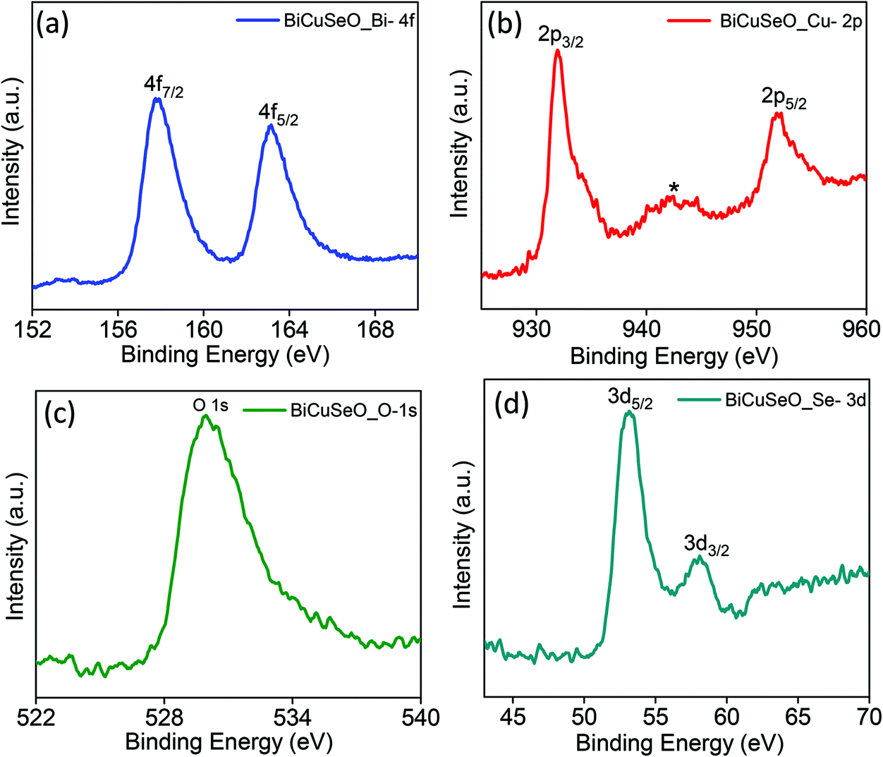 | ||
| Fig. 2 X-ray photoelectron spectra of BiCuSeO nanosheets showing the (a) Bi 4f, (b) Cu 2p, (c) O 1s and (d) Se 3d peaks. An additional peak (* marked) in the Cu 2p XPS spectrum is attributed to the presence of a small amount of Cu(II) at the surface. | ||
FESEM, TEM and AFM microscopy studies have been performed to understand the nanoscale morphology and the structure of the synthesized BiCuSeO sample. The FESEM image reveals the 2D nanosheet morphology of the sample (Fig. 3a). EDAX analysis of the BiCuSeO sample indicates the presence of Bi, Cu, Se and O (inset of Fig. 3a). The weight percentage (wt%) and atomic percentage (at%) of all the elements present in BiCuSeO, calculated from EDAX analysis, are given in Table 1. The TEM micrograph further confirms the thin nanosheet morphology of the synthesised BiCuSeO (Fig. 3b and c). The lateral dimensions of the nanosheets range from 0.5 to 1 μm. The selected-area electron diffraction (SAED) pattern taken from a single sheet region depicts the single crystalline nature of the BiCuSeO nanosheets (inset of Fig. 3b). The inset of Fig. 3c shows a TEM image of the bent edges of BiCuSeO, which indicate the stacking of a few nanosheets, one over another. A high resolution TEM (HRTEM) image (Fig. 3d) of the BiCuSeO nanosheets shows a clear lattice spacing of 2.67 Å, which corresponds to the (111) interplanar distance of tetragonal BiCuSeO. The ultra-thin nature of the nanosheets was further confirmed by AFM (inset of Fig. 3d). The height profile obtained from a typical AFM micrograph indicates that a thickness of ∼3.4 nm corresponds to 4 layers of BiCuSeO with a lateral dimension of ∼1 μm. Fig. 3e shows the scanning transmission electron microscopy (STEM) image of the BiCuSeO nanosheets. Additionally, EDAX elemental mapping analysis on a selected area of the BiCuSeO nanosheets (Fig. 3e), which is presented in Fig. 3f, points out the homogeneous distribution of all the elements in the BiCuSeO nanosheets.
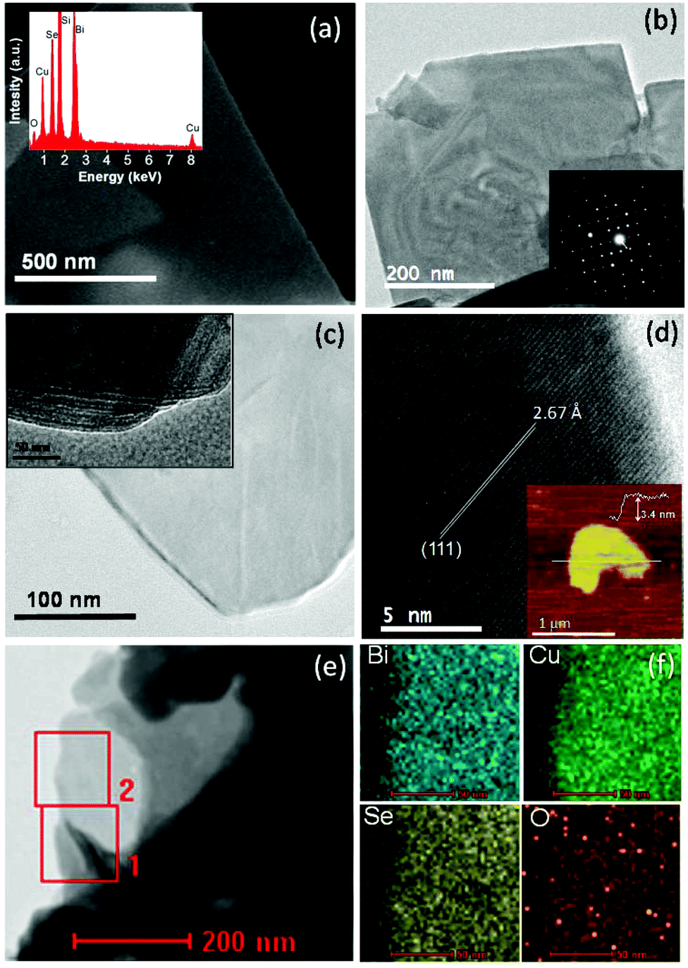 | ||
| Fig. 3 (a) FESEM image of the BiCuSeO nanosheets. The inset in (a) shows the EDAX of the BiCuSeO nanosheets. (b) TEM image of the BiCuSeO nanosheets. The inset of (b) shows the SAED pattern of a single nanosheet. (c) Another TEM image of the BiCuSeO nanosheets. Inset of (c) shows the bent edges of several BiCuSeO nanosheets which are stacked one over another. (d) HRTEM image of the BiCuSeO nanosheets showing the crystalline nature and spacing between (111) planes. The inset of (d) demonstrates an AFM image of the BiCuSeO nanosheets and the height profile showing a thickness of ∼3.4 nm. (e) STEM image of the BiCuSeO nanosheets (f) EDAX color mapping for Bi, Cu, Se and O in the BiCuSeO nanosheets during STEM imaging (from the highlighted portion (numbered as 2) of the STEM image). | ||
| Element | wt% | at% |
|---|---|---|
| O | 3.83 | 22.35 |
| Se | 21.82 | 25.81 |
| Bi | 56.15 | 25.09 |
| Cu | 18.2 | 26.75 |
| Total | 100 | 100 |
The layered structure and low thermal conductivity of bulk BiCuSeO motivate us to measure the thermoelectric properties of the BiCuSeO nanosheets. In order to measure thermoelectric properties, pellets of the BiCuSeO nanosheets were made by hot pressing of the as synthesized nanosheet powder sample. Fig. 4 represents the temperature dependent thermoelectric properties of the BiCuSeO nanosheets. Temperature dependent electrical conductivity (σ) and the Seebeck coefficient (S) of the BiCuSeO nanosheets are shown in Fig. 4a. BiCuSeO nanosheets show superior σ values to the bulk sample throughout the measured temperature range (Fig. S3a‡).20 We have measured the p-type carrier in BiCuSeO to be ∼3.8 × 1018 cm−3 at room temperature, which is higher than that of the bulk BiCuSeO.20 We have estimated the carrier mobility (μ) in BiCuSeO nanosheets using the formula σ = nheμ, where e is the electronic charge. The estimated carrier mobility value is ∼25 cm2 V−1 s−1, which is slightly higher than that of the bulk pristine BiCuSeO (22 cm2 V−1 s−1).20 This is attributed to the increase in electrical conductivity in the nanosheet sample compared to that in the bulk.20 At room temperature, a σ value of ∼15 S cm−1 was measured for the BiCuSeO nanosheets, and remains almost the same with a value of ∼13 S cm−1 at 722 K. The positive value of S depicts p-type conduction in the BiCuSeO nanosheets. An S value of ∼223 μV K−1 is measured at room temperature which increases to ∼267 μV K−1 at 722 K (Fig. 4a). Although the S value for the nanosheets is lower than that of the bulk sample (due to an increase in the carrier concentration in the nanosheet sample), a large increase in the σ value resulted in a significant improvement of the average power factor (σS2) in the nanosheet sample compared to that in its bulk counterpart20 (see Fig. S3c, ESI‡).
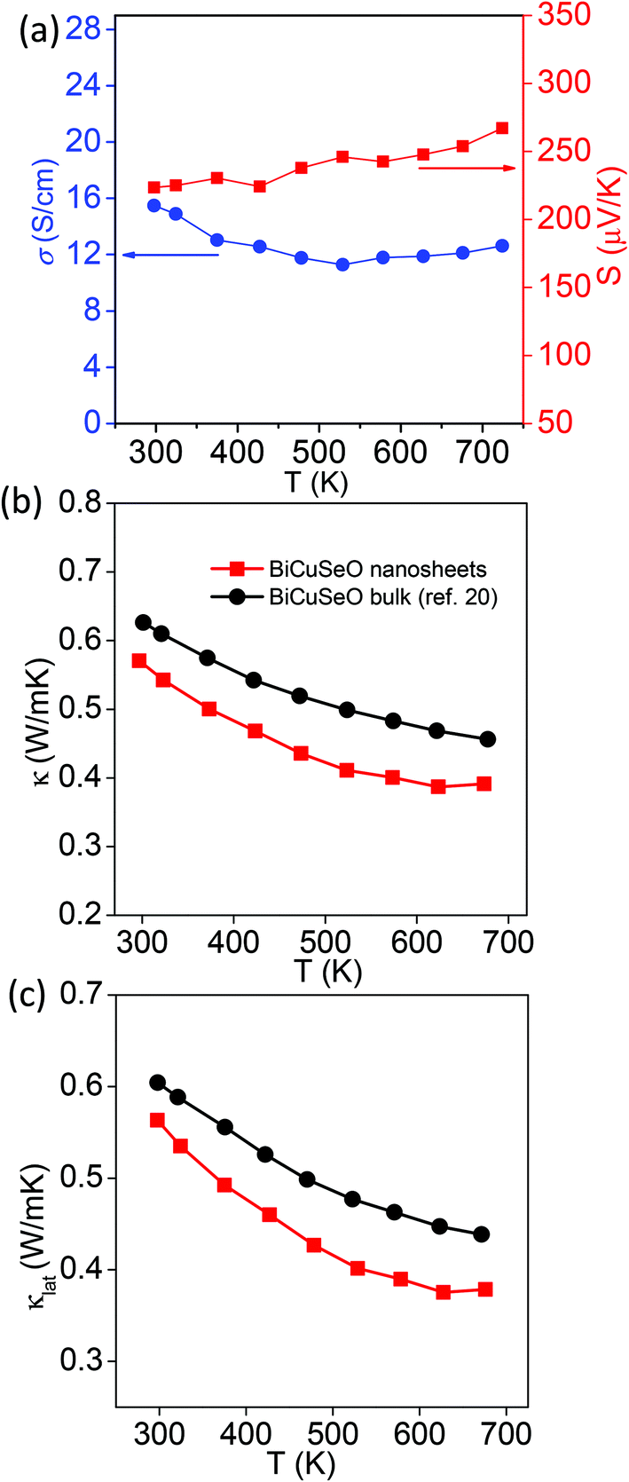 | ||
| Fig. 4 (a) Temperature dependent Seebeck coefficient (S) and electrical conductivity (σ) of the BiCuSeO nanosheets. Temperature dependent (b) total thermal conductivity (κ) and (c) lattice thermal conductivity (κlat) of the BiCuSeO nanosheets and bulk BiCuSeO.20 | ||
The total thermal conductivity (κ) of the BiCuSeO nanosheet sample in the range of 300–700 K along with κ of the previously reported bulk sample20 are presented in Fig. 4b, whereas thermal diffusivity (D) and Cp values of the BiCuSeO nanosheets are presented in Fig. S4, ESI.‡ We found that the BiCuSeO nanosheets exhibit a lower κ value throughout the measured temperature range compared to the bulk counterpart. A κ value of ∼0.56 W m−1 K−1 was measured at room temperature, which further decreased to 0.4 W m−1 K−1 at 675 K. The large decrease in temperature dependent κ compared to the bulk sample is attributed to the significant reduction of the lattice thermal conductivity (κlat) in BiCuSeO nanosheets (Fig. 4c). The κlat of BiCuSeO nanosheets is obtained by subtracting electrical thermal conductivity (κel) from the total thermal conductivity (κ), whereas κel is calculated using the Wiedemann–Franz law, κel = LσT, where L is the Lorenz number. L is derived by the fitting of the respective Seebeck coefficients, which estimate the reduced chemical potential assuming a single parabolic band, which is described elsewhere.37 Such a low κlat in the nanosheet sample originates from phonon scattering by the nano/meso-scale interfaces and grains in the hot pressed samples in addition to the interfaces of the layers and bond anharmonicity in the bulk BiCuSeO. A thermoelectric figure of merit (zT) value was estimated to be 0.2 at 722 K for the BiCuSeO nanosheet, which is higher than that of the bulk sample20 at that temperature.
Conclusions
In conclusion, we have synthesized few layered ultrathin (3–4 nm thick and ∼1 μm long) nanosheets of BiCuSeO for the first time using a simple, high yielding and surfactant-free soft chemical method. BiCuSeO nanosheets exhibit an optical band gap of ∼0.9 eV and p-type conduction. The nanosheet sample exhibits superior electronic transport and low lattice thermal conductivity compared to the bulk sample in the measured temperature range. BiCuSeO nanosheets show a higher average σS2 in the 300–723 K range than that of the bulk sample due to higher electronic conductivity compared to bulk BiCuSeO. Furthermore, low lattice thermal conductivity in the BiCuSeO nanosheets originates from extensive phonon scattering from the nano/meso-scale interfaces and grain boundaries in addition to the interfaces of the layers and bond anharmonicity of the bulk BiCuSeO. Thus, pristine nanosheets of BiCuSeO demonstrate promising potential application in thermoelectric energy harvesting. We would like to note that the nanosheet sample used in the present study is not doped and hence the performance of these nanoheets could be further improved by aliovalent chemical doping in the future.Acknowledgements
This work was supported by SERB, DST (EMR/2016/000651), the New Chemistry Unit and the Sheikh Saqr Laboratory. M. S. thanks UGC for her research fellowship. S. N. G. acknowledges JNCASR for his research fellowship.References
- K. S. Novoselov, V. I. Falko, L. Colombo, P. R. Gellert, M. G. Schwab and K. Kim, Nature, 2012, 490, 192 CrossRef CAS PubMed.
- K. S. Novoselov, A. Mishchenko, A. Carvalho and A. H. C. Neto, Science, 2016, 353, 461 CrossRef CAS PubMed.
- M. Chhowalla, H. S. Shin, G. Eda, L. J. Li, K. P. Loh and H. Zhang, Nat. Chem., 2013, 5, 263 CrossRef PubMed.
- (a) Y. Liu, C. Xiao, Z. Li and Y. Xie, Adv. Energy Mater., 2016 DOI:10.1002/aenm.201600436; (b) Y. Sun, S. Gao and Y. Xie, Chem. Soc. Rev., 2014, 43, 530 RSC.
- C. Tan and H. Zhang, Nat. Commun., 2015, 6, 7873 CrossRef CAS PubMed.
- H. Zhang, ACS Nano, 2015, 9, 9451 CrossRef CAS PubMed.
- C. N. R. Rao, H. S. S. R. Matte and U. Maitra, Angew. Chem., Int. Ed., 2013, 52, 13162 CrossRef CAS PubMed.
- (a) X. Cao, C. Tan, X. Zhang, W. Zhao and H. Zhang, Adv. Mater., 2016, 28, 6167 CrossRef CAS PubMed; (b) L. Nie, Y. Zhang, W.-W. Xiong, T.-T. Lim, R. Xu, Q. Yan and Q. Zhang, Inorg. Chem. Front., 2016, 3, 111 RSC; (c) J. Gao, Q. Tay, P.-Z. Li, W.-W. Xiong, Y. Zhao, Z. Chen and Q. Zhang, Chem. – Asian J., 2014, 9, 131 CrossRef CAS PubMed.
- (a) G. Tan, L. Zhao and M. G. Kanatzidis, Chem. Rev., 2016, 116, 12123 CrossRef CAS PubMed; (b) W. G. Zeier, A. Zevalkink, Z. M. Gibbs, G. Hautier, M. G. Kanatzidis and G. J. Snyder, Angew. Chem., Int. Ed., 2016, 55, 2 CrossRef PubMed; (c) L. D. Zhao, V. P. Dravid and M. G. Kanatzidis, Energy Environ. Sci., 2014, 7, 251 RSC; (d) Y. Sun, S. Gao, F. Lei, C. Xiao and Y. Xie, Acc. Chem. Res., 2015, 48, 3 CrossRef CAS PubMed.
- (a) K. Biswas, J. He, I. D. Blum, C. I. Wu, T. P. Hogan, D. N. Seidman, V. P. Dravid and M. G. Kanatzidis, Nature, 2012, 489, 414 CrossRef CAS PubMed; (b) K. Biswas, J. He, Q. Zhang, G. Wang, C. Uher, V. P. Dravid and M. G. Kanatzidis, Nat. Chem., 2011, 3, 160 CrossRef CAS PubMed.
- (a) A. Banik, U. S. Shenoy, S. Saha, U. V. Waghmare and K. Biswas, J. Am. Chem. Soc., 2016, 138, 13068 CrossRef CAS PubMed; (b) A. Banik, B. Vishal, S. Perumal, R. Datta and K. Biswas, Energy Environ. Sci., 2016, 9, 2011 RSC; (c) M. K. Jana, K. Pal, U. V. Waghmare and K. Biswas, Angew. Chem., Int. Ed., 2016, 55, 7592 Search PubMed; (d) S. Roychowdhury, U. S. Shenoy, U. V. Waghmare and K. Biswas, Angew. Chem., Int. Ed., 2015, 54, 15241 CrossRef CAS PubMed; (e) S. N. Guin, J. Pan, A. Bhowmik, D. Sanyal, U. V. Waghmare and K. Biswas, J. Am. Chem. Soc., 2014, 136, 12712 CrossRef CAS PubMed.
- B. Poudel, Q. Hao, Y. Ma, Y. Lan, A. Minnich, B. Yu, X. Yan, D. Wang, A. Muto, D. Vashaee, X. Chen, J. Liu, M. S. Dresselhaus, G. Chen and Z. Ren, Science, 2008, 320, 634 CrossRef CAS PubMed.
- S. Kim, K. H. Lee, H. A. Mun, H. S. Kim, S. W. Hwang, J. W. Roh, D. J. Yang, W. Ho Shin, X. S. Li, Y. H. Lee, G. J. Snyder and S. W. Kim, Science, 2015, 348, 109 CrossRef CAS PubMed.
- R. J. Mehta, Y. Zhang, C. Karthik, B. Singh, R. W. Siege, T. B. Tasciuc and G. Ramanath, Nat. Mater., 2012, 11, 233 CrossRef CAS PubMed.
- L. D. Zhao, S. H. Lo, Y. Zhang, H. Sun, G. Tan, C. Uher, C. Wolverton, V. P. Dravid and M. G. Kanatzidis, Nature, 2014, 508, 373 CrossRef CAS PubMed.
- L. D. Zhao, G. Tan, S. Hao, J. He, Y. Pei, H. Chi, H. Wang, S. Gong, H. Xu, V. P. Dravid, C. Uher, G. J. Snyder, C. Wolverton and M. G. Kanatzidis, Science, 2016, 351, 141 CrossRef CAS PubMed.
- K. Peng, X. Lu, H. Zhan, S. Hui, X. Tang, G. Wang, J. Dai, C. Uher, G. Wang and X. Zhou, Energy Environ. Sci., 2016, 9, 454 CAS.
- S. D. N. Luu and P. Vaqueiro, J. Materiomics, 2016, 2, 131–140 CrossRef.
- A. M. Kusainova, P. S. Berdonosov, L. G. Akselrud, L. N. Kholodkovskaya, V. A. Dolgikh and B. A. Popovkin, J. Solid State Chem., 1994, 112, 189 CrossRef CAS.
- L. D. Zhao, J. He, D. Berardan, Y. Lin, J. F. Li, C. W. Nanc and N. Dragoe, Energy Environ. Sci., 2014, 7, 2900 CAS.
- (a) Y. Liu, L. D. Zhao, Y. Liu, J. Lan, W. Xu, F. Li, B. P. Zhang, D. Berardan, N. Dragoe, Y. H. Lin, C. W. Nan, J. F. Li and H. Zhu, J. Am. Chem. Soc., 2011, 133, 20112 CrossRef CAS PubMed; (b) Z. Li, C. Xiao, S. Fan, Y. Deng, W. Zhang, B. Ye and Y. Xie, J. Am. Chem. Soc., 2015, 137, 6587 CrossRef CAS PubMed.
- E. S. Stampler, W. C. Sheets, M. I. Bertoni, W. Prellier, T. O. Mason and K. R. Poeppelmeier, Inorg. Chem., 2008, 47, 10009 CrossRef CAS PubMed.
- J. Li, J. Sui, C. Barreteau, D. Berardan, N. Dragoe, W. Cai, Y. Pei and L. D. Zhao, J. Alloys Compd., 2013, 551, 649–653 CrossRef CAS.
- Y. L. Pei, J. He, J. F. Li, F. Li, Q. Liu, W. Pan, C. Barreteau, D. Berardan, N. Dragoe and L. D. Zhao, NPG Asia Mater., 2013, 5, e47 CrossRef CAS.
- C. Barreteau, D. B. Rardan, E. Amzallag, L. D. Zhao and N. Dragoe, Chem. Mater., 2012, 24, 3168 CrossRef CAS.
- J. L. Lan, Y. C. Liu, B. Zhan, Y. H. Lin, B. Zhang, X. Yuan, W. Zhang, W. Xu and C. W. Nan, Adv. Mater., 2013, 25, 5086 CrossRef CAS PubMed.
- D. Yang, X. Su, Y. Yan, T. Hu, H. Xie, J. He, C. Uher, M. G. Kanatzidis and X. Tan, Chem. Mater., 2016, 28, 4628 CrossRef CAS.
- J. S. Son, M. K. Choi, M. K. Han, K. Park, J. Y. Kim, S. J. Lim, M. Oh, Y. Kuk, C. Park, S. J. Kim and T. Hyeon, Nano Lett., 2012, 12, 640 CrossRef CAS PubMed.
- Y. Sun, H. Cheng, S. Gao, Q. Liu, Z. Sun, C. Xiao, C. Wu, S. Wei and Y. Xie, J. Am. Chem. Soc., 2012, 134, 20294 CrossRef CAS PubMed.
- M. K. Jana, K. Biswas and C. N. R. Rao, Chem. – Eur. J., 2013, 19, 9110 CrossRef CAS PubMed.
- Y. Zhao, R. W. Hughes, Z. Su, W. Zhou and D. H. Gregory, Angew. Chem., Int. Ed., 2011, 50, 10397 CrossRef CAS PubMed.
- A. Chatterjee and K. Biswas, Angew. Chem., Int. Ed., 2015, 54, 5623 CrossRef CAS PubMed.
- A. Chatterjee, S. N. Guin and K. Biswas, Phys. Chem. Chem. Phys., 2014, 16, 14635 RSC.
- G. Han, S. R. Popuri, H. F. Greer, J. W. G. Bos, W. Zhou, A. R. Knox, A. Montecucco, J. Siviter, E. A. Man, M. Macauley, D. J. Paul, W. Li, M. C. Paul, M. Gao, T. Sweet, R. Freer, F. Azough, H. Baig, N. Sellami, T. K. Mallick and D. H. Gregory, Angew. Chem., Int. Ed., 2016, 55, 6433 CrossRef CAS PubMed.
- S. Saha, A. Banik and K. Biswas, Chem. – Eur. J., 2016, 22, 15634 CrossRef CAS PubMed.
- S. N. Guin, D. Sanyal and K. Biswas, Chem. Sci., 2016, 7, 534 RSC.
- (a) L. D. Zhao, S. H. Lo, J. He, H. Li, K. Biswas, J. Androulakis, C. I. Wu, T. P. Hogan, D. Y. Chung, V. P. Dravid and M. G. Kanatzidis, J. Am. Chem. Soc., 2011, 133, 20476 CrossRef CAS PubMed; (b) W. S. Liu, Q. Zhang, Y. Lan, S. Chen, X. Yan, Q. Zhang, H. Wang, D. Wang, G. Chen and Z. Ren, Adv. Energy Mater., 2011, 1, 577 CrossRef CAS; (c) A. F. May, E. S. Toberer, A. Saramat and G. J. Snyder, Phys. Rev. B: Condens. Matter Mater. Phys., 2009, 80, 125205 CrossRef.
Footnotes |
| † We dedicate this paper to Prof. Mercouri G. Kanatzidis on his 60th birthday. |
| ‡ Electronic supplementary information (ESI) available. See DOI: 10.1039/C6QI00435K |
| This journal is © the Partner Organisations 2017 |