
 Open Access Article
 This Open Access Article is licensed under a
 Creative Commons Attribution 3.0 Unported Licence
Electronic properties of single-layer tungsten disulfide on epitaxial graphene on silicon carbide†
Stiven
Forti
 *a,
Antonio
Rossi
ab,
Holger
Büch
a,
Tommaso
Cavallucci
b,
Francesco
Bisio
c,
Alessandro
Sala
d,
Tevfik Onur
Menteş
d,
Andrea
Locatelli
d,
Michele
Magnozzi
e,
Maurizio
Canepa
e,
Kathrin
Müller
f,
Stefan
Link
f,
Ulrich
Starke
f,
Valentina
Tozzini
b and
Camilla
Coletti
ag
*a,
Antonio
Rossi
ab,
Holger
Büch
a,
Tommaso
Cavallucci
b,
Francesco
Bisio
c,
Alessandro
Sala
d,
Tevfik Onur
Menteş
d,
Andrea
Locatelli
d,
Michele
Magnozzi
e,
Maurizio
Canepa
e,
Kathrin
Müller
f,
Stefan
Link
f,
Ulrich
Starke
f,
Valentina
Tozzini
b and
Camilla
Coletti
ag
aCenter for Nanotechnology Innovation @ NEST, Istituto Italiano di Tecnologia, Piazza San Silvestro 12, 56127 Pisa, Italy. E-mail: stiven.forti@iit.it
bNEST, Istituto Nanoscienze-CNR and Scuola Normale Superiore, Piazza S. Silvestro 12, 56127 Pisa, Italy
cCNR-SPIN, Corso F. Perrone 24, 16152 Genova, Italy
dElettra – Sincrotrone Trieste S.C.p.A., Basovizza, Trieste 34149, Italy
eOPTMATLAB and Dipartimento di Fisica, Universitá degli Studi di Genova, via Dodecaneso 33 16146, Genova, Italy
fMax-Planck-Institut für Festkörperforschung, Heisenbergstr. 1, D-70569 Stuttgart, Germany
gGraphene Labs, Istituto Italiano di Tecnologia, via Morego 30, 16163 Genova, Italy
First published on 23rd October 2017
Abstract
This work reports an electronic and micro-structural study of an appealing system for optoelectronics: tungsten disulfide (WS2) on epitaxial graphene (EG) on SiC(0001). The WS2 is grown via chemical vapor deposition (CVD) onto the EG. Low-energy electron diffraction (LEED) measurements assign the zero-degree orientation as the preferential azimuthal alignment for WS2/EG. The valence-band (VB) structure emerging from this alignment is investigated by means of photoelectron spectroscopy measurements, with both high space and energy resolution. We find that the spin–orbit splitting of monolayer WS2 on graphene is of 462 meV, larger than what is reported to date for other substrates. We determine the value of the work function for the WS2/EG to be 4.5 ± 0.1 eV. A large shift of the WS2 VB maximum is observed as well, due to the lowering of the WS2 work function caused by the donor-like interfacial states of EG. Density functional theory (DFT) calculations carried out on a coincidence supercell confirm the experimental band structure to an excellent degree. X-ray photoemission electron microscopy (XPEEM) measurements performed on single WS2 crystals confirm the van der Waals nature of the interface coupling between the two layers. In virtue of its band alignment and large spin–orbit splitting, this system gains strong appeal for optical spin-injection experiments and opto-spintronic applications in general.
1 Introduction
In recent times, combining two-dimensional (2D) materials with different properties in order to obtain novel van der Waals (vdW) heterostacks with tailored and tunable features1 has become a possible and tantalizing goal. At present, the most successfully combined 2D materials have been graphene and hexagonal boron nitride (h-BN). The latter provides a great substrate for enhancing graphene's electrical properties and the encapsulation of graphene within h-BN has been proved to be very effective in doing this.2,3 However, 2D encapsulating layers alternative to h-BN, with better prospects in terms of synthesis and scalability and which might open novel research avenues are being actively seeked for. In this respect, tungsten disulfide (WS2) combined with graphene is a vdW heterostack which hosts a great appeal for applications in optoelectronics. For example, the mobility of graphene encapsulated between WS2 and h-BN is very promising,4i.e. about 60![[thin space (1/6-em)]](https://www.rsc.org/images/entities/char_2009.gif) 000 cm2 V−1 s−1. Improving the mobility of graphene by providing an extremely flat substrate and a defect-free interface is only one possible application out of plenty that might emerge. WS2 has a layer-number dependent band gap and when going from 2 to 1 layer, it exhibits a transition from indirect- to direct-gap semiconductor.5,6 The gap in single layer WS2 measures about 2.1 eV (ref. 5, 7 and 8) at the two non-equivalent
000 cm2 V−1 s−1. Improving the mobility of graphene by providing an extremely flat substrate and a defect-free interface is only one possible application out of plenty that might emerge. WS2 has a layer-number dependent band gap and when going from 2 to 1 layer, it exhibits a transition from indirect- to direct-gap semiconductor.5,6 The gap in single layer WS2 measures about 2.1 eV (ref. 5, 7 and 8) at the two non-equivalent ![[K with combining overline]](https://www.rsc.org/images/entities/i_char_004b_0305.gif) -points of its Brillouin Zone (BZ). The neutral exciton in WS2 has a large binding energy,9 making it a good candidate for the realization of exciton-polariton lasers.10 In virtue of such a long-lived exciton, WS2 shows a remarkably high room-temperature photoluminescence.11 In the vicinity of the two valleys the bands are energy separated because of spin–orbit coupling. The spin-valley coupling is robust enough to observe spontaneous magnetoluminescence at zero magnetic field.12 Combining semimetallic graphene and semiconducting single-layer WS2 in a vertical heterostack brings together massless Dirac particles with long spin-lifetimes and strongly spin-polarized electrons with great potential for spintronics and optospintronics. Indeed, when placed in close contact, these materials have already shown interesting results in this direction. The high spin–orbit interaction in WS2 bands has been observed to induce an enhancement of the intrinsic graphene spin–orbit coupling via proximity effect.13 Moreover, single-layer WS2 was observed to preserve the polarization in photoluminescence experiments.14 Charge transfer between WS2 and graphene was seen to be fast and efficient under optical pump.15 Very recently, a first evidence of tunable spin-injection for stacked flakes of WS2 and graphene has been reported.16 The system has therefore a serious appeal for a wide number of applications, ranging from photodetection17 to flexible and transparent electronics,18 to optospintronics.19 However, an in-depth investigation of its electronic properties is still missing.
-points of its Brillouin Zone (BZ). The neutral exciton in WS2 has a large binding energy,9 making it a good candidate for the realization of exciton-polariton lasers.10 In virtue of such a long-lived exciton, WS2 shows a remarkably high room-temperature photoluminescence.11 In the vicinity of the two valleys the bands are energy separated because of spin–orbit coupling. The spin-valley coupling is robust enough to observe spontaneous magnetoluminescence at zero magnetic field.12 Combining semimetallic graphene and semiconducting single-layer WS2 in a vertical heterostack brings together massless Dirac particles with long spin-lifetimes and strongly spin-polarized electrons with great potential for spintronics and optospintronics. Indeed, when placed in close contact, these materials have already shown interesting results in this direction. The high spin–orbit interaction in WS2 bands has been observed to induce an enhancement of the intrinsic graphene spin–orbit coupling via proximity effect.13 Moreover, single-layer WS2 was observed to preserve the polarization in photoluminescence experiments.14 Charge transfer between WS2 and graphene was seen to be fast and efficient under optical pump.15 Very recently, a first evidence of tunable spin-injection for stacked flakes of WS2 and graphene has been reported.16 The system has therefore a serious appeal for a wide number of applications, ranging from photodetection17 to flexible and transparent electronics,18 to optospintronics.19 However, an in-depth investigation of its electronic properties is still missing.
Here we report on the structural and electronic properties of the WS2/graphene system synthesized over large areas via CVD.14 Investigations are carried out using synchrotron-based X-ray photoemission electron microscopy (XPEEM) for chemical and electronic-structure characterisation, combined with structurally sensitive low-energy electron microscopy20 (LEEM). The electronic structure is further probed using angle-resolved photoelectron spectroscopy (ARPES), which provides higher energy resolution. The experimental results are supported by DFT calculations.
2 Methods
2.1 Experimental details
Nominally on-axis Si-face polished 6H-SiC(0001) purchased from SiCrystal GmbH was used as a substrate for all the experiments. Epitaxial graphene (EG) was grown by thermal decomposition, adapting the recipe of Emtsev and coworkers21 in an Aixtron Black Magic reaction chamber. WS2 was synthesized by CVD in a hot-wall quartz furnace, similar to the system described in ref. 22 (cf. also Fig. S9 in the ESI†), heating up WO3 powder at 900 °C for 1 hour and using thermally vaporized sulfur powder as precursor. Argon was used as carrier gas with a flow of 0.5 slm, while the pressure in the reactor was kept at 1 mbar.14The microscopy measurements were carried out at the Nanospectroscopy beamline (Elettra Synchrotron, Italy) using the Spectroscopic Photoemission and Low Energy Electron Microscope (SPELEEM) set-up. The SPELEEM combines LEEM with energy-filtered XPEEM. LEEM is a structure-sensitive technique which uses elastically backscattered electrons to image the surface. In the SPELEEM, a focused, collimated electron beam is generated by a LaB6 gun; the electron energy is precisely set by applying a voltage bias, referred to as start voltage (STV), to the sample.23 The lateral resolution of the microscope in LEEM is better than 10 nm.24,25 Along with imaging, microscopic low-energy electron diffraction (μLEED) measurements (also known as microprobe-LEED) are performed using illumination apertures to restrict the electron beam to a minimum size of 500 nm. The SPELEEM is equipped with a bandpass energy filter, allowing to carry out laterally resolved ultra-violet (UV) and soft X-ray photoelectron spectroscopy. In imaging mode, the lateral resolution approaches 30 nm, the energy resolution 300 meV. XPEEM data at core level energies were evaluated to obtain microscopic photoelectron spectroscopy (μXPS) spectra. The system is illuminated with photons linearly polarized in the synchrotron's ring plane. The sample is mounted vertical with respect to that plane and the photon beam impinge at 16° onto the sample. The light is therefore mostly p-polarized. The SPELEEM allows also to carry out microprobe (also known as microspot) ARPES (μARPES) measurements.26 With this technique the band structure of the system can be probed on areas as small as ∼2 μm in diameter, allowing the imaging of the angular distribution of photoemitted electrons.
In order to resolve the spin–orbit splitting of the WS2 bands at the -point, we carried out ARPES measurements at the Max Planck Institute (MPI) for Solid State Research in Stuttgart. There, ARPES spectra were recorded with a hemispherical SPECS Phoibos 150 electron analyzer in combination with a Scienta VUV5000 lamp. A monochromator selects the He I emission line of the lamp (21.22 eV). 2D dispersion sets E(k) were recorded with the display detector, through a 0.2 mm entrance slit in low angular dispersion mode, corresponding to ±13° range. With this technique the probed area is of the order of 1 mm2. The mapping of the WS2 BZ was done by measuring single spectra perpendicularly to the high-symmetry direction and varying the photoemission angle. The spectra were acquired at different azimuthal orientations along the Γ–, Γ–![[M with combining overline]](https://www.rsc.org/images/entities/i_char_004d_0305.gif) , – directions. The three different band branches were then put together via software. In this geometrical configuration, the graphene π-bands intersect the WS2 VB for a small portion. Considering their low cross section at 21 eV and the high emission angle needed close to , the π-bands are not to be seen unless the contrast is strongly enhanced, as in the inset Fig. 2(e).
, – directions. The three different band branches were then put together via software. In this geometrical configuration, the graphene π-bands intersect the WS2 VB for a small portion. Considering their low cross section at 21 eV and the high emission angle needed close to , the π-bands are not to be seen unless the contrast is strongly enhanced, as in the inset Fig. 2(e).
X-ray photoelectron spectroscopy (XPS) spectra were acquired with a Kratos hemispherical analyzer coupled to a monochromatized Al Kα X-ray source. The atomic force microscopy (AFM) images were acquired with a Bruker Dimension Icon microscope used in ScanAsyst tapping mode. Spatially averaged LEED measurements were carried out using an ErLEED system from SPECS GmbH.
All measurements were performed at room temperature.
2.2 Core-level fitting procedures
In section 3.3 we display the results of local XPEEM measurements. For those measurements, photons at 400 eV were used. For every spectrum a Shirley-type background was considered. We used the reference position of the C 1s peak of SiC in monolayer graphene (MLG) on SiC(0001) (i.e., 283.7 eV (ref. 27)), in order to align the binding energy of the spectra extracted for the XPEEM scans. The symmetric peaks were fitted with Voigt functions. To take into account the asymmetry of the peaks coming from conductive layers, such as graphitic carbon, a Doniach-Šunjić (DS) line shape was used. The C 1s on MLG was fitted taking into account the following components: SiC (Voigt), graphene (DS), S1 (Voigt) and S2 (Voigt), where S1 and S2 are the components associated with the buffer layer.27–292.3 Computational methods
The electronic band structure of the system was evaluated within the Density Functional Theory (DFT) framework, using the code Quantum ESPRESSO.30 The simulation setup is similar to the one we previously used and tested for similar systems.31 We used a plane wave expansion of the wavefunctions within the pseudopotential32,33 approach and a PBEsol34 vdW corrected35 density functional, both scalar and fully relativistic for spin orbit calculations, using a calculation setup which was previously well tested in similar systems.31,36 Both the isolated (i.e. free-standing) WS2 and WS2 on top of graphene were studied. To match the graphene and WS2 lattice parameters a supercell was used, with a periodicity of (7 × 7) with respect to WS2 and (9 × 9) with respect to graphene. At variance with a similar previous calculations37 we included vdW correction, which were proven of utmost importance in reproducing inter-layer interactions in graphene-based systems.31 The model systems, the supercells and all the simulation setup information are described in detail in the ESI.†3 Results and discussion
3.1 Structure and morphology
Fig. 1(a) displays a representative image of the typical μm-sized triangularly-shaped WS2 single-crystals obtained with our growth approach. This LEEM micrograph, acquired over a field of view (FOV) of 30 μm, indicates that the majority of the WS2 crystals are aligned along the same crystallographic direction. In Fig. 1(b) we show an AFM image with a WS2 triangle to highlight the morphology of the system. The average height of the single-layer WS2 is estimated to be 0.84 nm. The LEEM micrograph in panel (c) is a zoom-in of the image of panel (a) on a single triangle over a 6 μm FOV. The different contrast results from the different electron energy used (STV 4.8 instead of 3.2 V of (a)). μLEED measurements were performed on the same region, the results of which are shown in panels (d) and (e) for WS2 and graphene, respectively. Because of the very low intensity of the graphene spots when measured on the triangle, we show a measurement acquired outside of the triangle, on a MLG region nearby it. Both measured regions are indicated with dashed circles on the figure. In μLEED, the (10) spots of WS2 are 3-fold symmetric, resulting from the broken inversion symmetry of the real space lattice, as visible from the sketch in panel (g). In spatially averaged LEED measurements shown in panel (f), the 3-fold symmetry is lost because of the presence of crystals rotated by nπ/3, as visible in panel (a). The preferential alignment of the WS2 along the graphene's crystalline axes is apparent by looking at the (10) diffraction spots of WS2, indicated by wi,j in the figure. The minority orientations are visible as a ring passing through the (10) spots of WS2. The ring is very faint in intensity and its diameter is slightly smaller – about 2.6% – than the SiC reciprocal lattice vectors (si,j in the figure). Moreover, the (10) spots of WS2 appear to be slightly elongated along the azimuthal direction, possibly suggesting an equilibrium position fluctuating about the zero degrees orientation. In panel (g) we display the 2D projection of the real and reciprocal space structures of the system as derived from the μLEED and LEED measurements, assuming the equilibrium value of the graphene's lattice parameter to be 2.461 Å and that of SiC to be 3.08 Å. We find the WS2 lattice parameter to be 3.16 ± 0.1 Å. However, no evidence of superperiodicity (moiré pattern) was found in μLEED (at higher energies as well), in contrast with WS2/Au(111).38 From diffraction measurements we also determine that the edges of the triangular WS2 crystals on epitaxial graphene are aligned along the [1,0] (zigzag) direction, as apparent by comparing panels (c) and (g).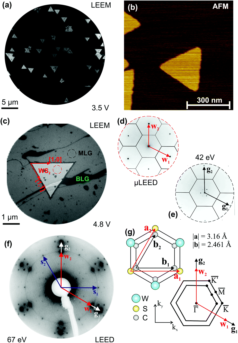 | ||
| Fig. 1 (a) LEEM micrograph recorded at STV 3.5 eV on a 30 μm FOV. (b) AFM image centered on a single WS2 triangle on MLG over a (770 × 770) nm2 area. (c) LEEM micrograph of a single WS2 crystal imaged at STV 4.8 eV on a 6 μm FOV. Areas with different contrast are labeled MLG, BLG and WS2, respectively. (d) and (e) μLEED pattern acquired on the dashed-circle areas for WS2 and MLG, respectively. (f) LEED pattern at electron energy of 67 eV. WS2, graphene and SiC reciprocal lattice vectors are indicated as w, g and s, respectively. (g) Real and reciprocal space sketch derived from μLEED. Crystal directions are drawn in panel (c), according to this sketch. | ||
3.2 Electronic properties
The band structure of WS2/MLG was measured by means of μARPES on a single WS2 crystal. In particular, the results for the triangle of Fig. 1(c) obtained with photons of 70 eV are shown in Fig. 2(a). The graphene π- and π*-bands are well visible and also highlighted by orange dots, corresponding to the DFT calculated bands on the graphene single cell. Calculated graphene σ-bands are not superimposed as in the experimental data they are not detectable due to their low intensity. The bands visible in Γ belong to WS2 as also indicated by DFT calculations (see Fig. S4 and S6 in the ESI†). Interestingly, at the points where the bands of graphene and WS2 cross (indicated by green arrows in the panel), no apparent splitting or gap is observed. In order to confirm this finding, DFT calculations were carried out, the result of which is summarized in Fig. 2(b), where we display the bands “unfolded” onto graphene's BZ, for better readability. The smallest coincidence lattice for the WS2/graphene system was found to be (7 × 7) WS2 unit cells (u.c.) on (9 × 9) of graphene, as sketched in Fig. 2(c). DFT calculations were carried out on this supercell and as a result, no mini-gap opening was predicted for this system (cf. Fig. S4 in the ESI† for further details), contrary to what was recently observed for MoS2 on graphene.39 However, the calculations predict that a gap of about 4 meV can be opened at the Dirac point when the distance between WS2 and graphene becomes small enough (see ESI†), a result which might open interesting scenarios for low-temperature measurements. To better match the experimental data the DFT spectrum was artificially “doped” by an energy shift of about 200 meV. The results of the calculations displayed in panel (b) do not include matrix-element effects depending on the incident photons and thus the intensity distribution cannot be directly compared with the experimental ARPES data. To better visualize the relation between the graphene π-bands and the WS2 bands, we show constant energy surfaces (CESs) in Fig. 2(d), extracted starting from the Fermi surface (FS) at binding energies indicated in the figure. The CESs in this case are small volumes in k space integrated over about 250 meV, corresponding to the resolution of the instrument. The data were acquired with a photon energy of 27.5 eV in order to maximize the intensity of the WS2 bands with respect to graphene (see Fig. S6†).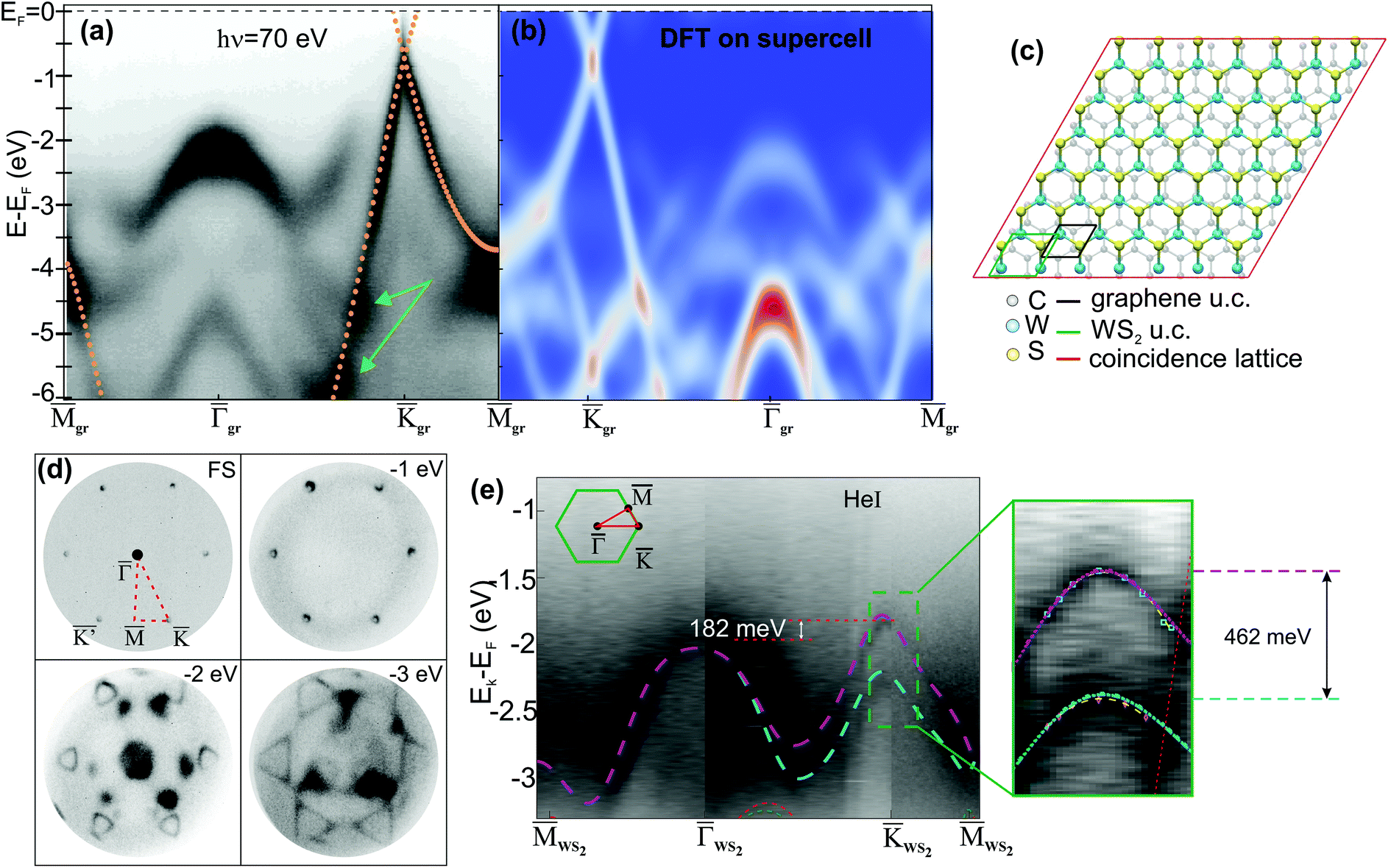 | ||
| Fig. 2 Band structure of WS2/MLG. (a) μARPES measured on a single WS2 triangle with photons of 70 eV. (b) Theoretical DFT band structure evaluated on the WS2/graphene supercell depicted in panel (c) and unfolded into graphene's BZ. (c) Coincidence supercell (7 × 7) over (9 × 9) of WS2/graphene. (d) Experimental ARPES CESs recorded with p-polarized photons at 27.5 eV (e) Experimental ARPES band structure of WS2/EG measured with He I light along the path indicated in the inset by the red line. DFT calculated bands including spin–orbit effects are overlapped to the raw data. On the right: zoom-in of the region around WS2 (green-dashed line in panel (e)). Both DFT calculated bands and experimental band fit are overimposed to the raw data. The red-dashed line is on the graphene's π-bands. | ||
We display the results of the ARPES measurements recorded at the MPI with He I radiation in Fig. 2(e), together with the DFT-calculated bands including spin–orbit coupling. The image was obtained by scanning the BZ of the system along the red line traced within the green hexagon in the inset (cf. Fig. S6(d) of the ESI† for the raw data). Note that in this image the high symmetry points are for the WS2 BZ, whereas for panels (a) and (b) we referred to graphene's BZ. Single spectra were measured perpendicular to the red line.
We have fitted the experimental data in proximity (±∼0.1 Å−1) of with a parabolic function in order to extract the effective mass values of the holes. The result along the Γ–– direction is displayed on the right side of Fig. 2(e), representing the zoom-in of the region framed with a green-dashed line in the panel. We find mh1 ≃ 0.39me for the low energy band and mh2 ≃ 0.53me for the high energy band, confirming the asymmetry reported in other publications.38
The spin–orbit splitting of the WS2 bands in was retrieved from integrated energy distribution curves (EDCs) to be 462 ± 5 meV (see also Fig. S7 in the ESI†). Notably, this value is about 10% larger than what was measured for monolayer WS2 on Au(111) and Ag(111)38,40 and about 7% larger than the highest value reported so far.41 The value measured on our system is comparable only with measurements carried out on bulk WS2.42
In Fig. 3(a) we show LEEM-IV spectra recorded on WS2, MLG and bilayer graphene (BLG) areas, as labeled in Fig. 1(c). LEEM-IV curves give information about the electronic properties of the system for energies above EF and their dips, at least in the case of graphene, indicate the number of layers.43–46 In the WS2 spectrum we observe three dips modulated by a linear decay of the intensity, possibly reflecting the three-layer structure of the single-layer WS2.
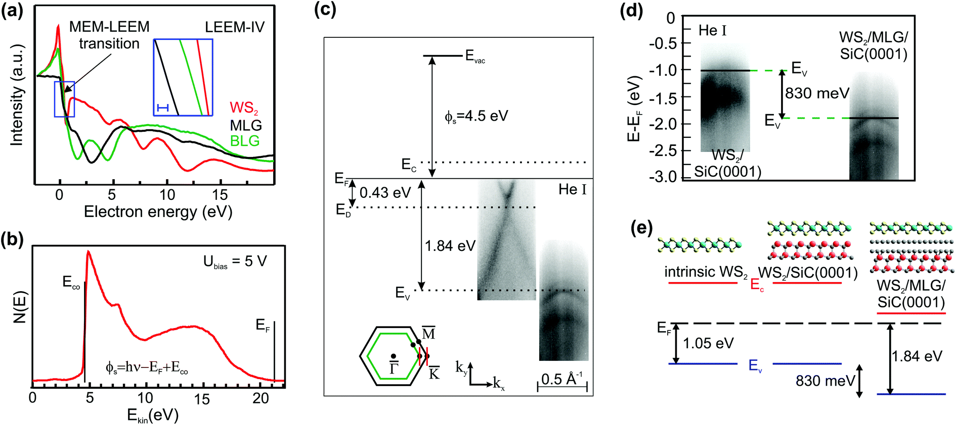 | ||
| Fig. 3 (a) LEEM-IV curves measured on and outside the triangle on the MLG, BLG and WS2 regions defined in Fig. 1(c). In the inset, the bar is 50 meV. (b) Experimental UPS data acquired with a 5 V bias voltage applied to the sample. (c) Scheme of the band alignment derived from the ARPES spectra measured with He I light along the red lines shown in the inset. (d) On the left, bands of WS2/SiC(0001) and on the right WS2/MLG/SiC(0001). Both measurements are aligned to the Fermi energy and the energy scale is the same. (e) Simple scheme of the different energy alignments for intrinsic (ideal) WS2, WS2/SiC(0001) and WS2/MLG. On the top, a schematic representation of each considered system. | ||
LEEM-IV curves can also provide a direct and local measurement of the surface potential difference between different regions looking at the transition between mirror mode (MEM) and LEEM.24 In the inset of the figure we show a zoom-in of the MEM-LEEM transition region with an energy scale-bar of 50 meV. We observe that the WS2/MLG exhibits a value of work function slightly larger (about 150 meV) than of pristine (or as grown) MLG. The value of the work function instead, was obtained over the entire sample from HeI UV photoelectron spectroscopy (UPS) measurements of the VB. The VB spectrum is shown in panel (b) and was acquired with the sample biased at 5 V in order to access the secondary electrons cut-off energy. The work function of the analyzer is constant and the acquisition software compensate for it in a way that the kinetic energy of the electrons at the Fermi level, essentially coincide with the photon energy. The work function of the sample ϕS is then hν − EF + Eco, where Eco is the cut-off energy beyond which no electron is emitted from the sample. The value obtained in this way is 4.35 ± 0.05 eV. By combining these information we could determine the band alignment of the system, which is displayed in Fig. 3(c).
Although the role of the substrate requires further investigation, in Fig. 3(d) we provide a first proof of its relevance. On the left side we show the ARPES spectrum of WS2 grown directly on 6H-SiC(0001) following the procedure described in section 2.1. The bands are recorded in in the same geometry as shown in the inset of panel (a). On the right side, we show again the ARPES of WS2/MLG as in panel (c). The energy difference between the two valence band maxima (Ev) is about 830 meV. This indicates that the WS2, when grown on SiC(0001), exhibits a band alignment very close to the one expected for isolated WS2, i.e. Fermi level in the middle of the bandgap. For the size of the bandgap we refer to recent time-resolved ARPES measurements,40 which set the bandgap value for single layer WS2 at 2.1 eV. To make this visually more clear, in panel (e) we show a scheme of the band alignment for the three situations: isolated WS2, WS2/SiC(0001) and WS2/MLG. On top of every sketch, a simple ball-stick model of each system is shown. For the WS2/MLG, the conduction band minimum (Ec) lays then ∼260 meV above the Fermi level. In the case of WS2/SiC(0001) instead, the valence band maximum (Ev) is found at 1.00 ± 0.05 eV below EF, which means that the donor states of the graphene/buffer layer system47,48 “pin” the Fermi level of WS2 on MLG, thereby lowering its work function. The spin–orbit splitting of the bands in remains instead unaltered. Indeed, for the WS2/SiC(0001), the ΔE between the fitted maxima of the peaks of the integrated intensity yields 458 ± 5 meV.
The population of the conduction band via transfer of negative charge to TMDs leads to unconventional phenomena as negative electronic compressibility (NEC), as observed in WSe249 and more recently also in WS2.41 The NEC reduces the size of the gap and since bilayer WS2 has a smaller band-gap, it could be readily metallic on EG, opening up the possibility for the observation of predicted exotic phenomena such as the transition to a superconductive phase.50,51 In addition, the energy difference between the maxima of the VB in Γ and is found to be ΔΓK = 182 meV (cf.Fig. 2(e)), about a third of what was observed for the same material on Au(111),38 possibly implying the occurrence of many-body renormalization effects of the bands or due to the graphene–WS2 interaction. As a comparison, we note that for the WS2/SiC(0001) system the same quantity was found to be ΔΓK = (250 ± 20) meV (not shown).
Despite the recent popularity of vdW vertical heterostructures and the variety of investigated TMDs, the system presented and studied in this work represents an unicum as referred to the potential applications in opto-spintronics. Graphene has a large spin relaxation time,52 but the electrical injection of spin in graphene suffers of problems arising from the quality of the contacts, defects at the interfaces, minority spin injection or the definition of a tunnel barrier to minimize it.53 A cleaner way to inject spin polarized carriers into graphene would be optically, i.e. by exploiting the optical selection rules introduced by the use of photons with a specific helicity. We propose that the WS2/MLG described in this work has the ideal band alignment for such applications using photons in the visible range.
3.3 Chemical properties
The chemical properties of the system are investigated locally, i.e. measuring each core level spectrum on and outside a single WS2 crystal, by means of XPEEM. The outcome of those measurements are summarized in Fig. 4(a–e). Laterally averaged chemical properties were instead collected via XPS, as described in the methods section and the data are summarized in Fig. S8 of the ESI.†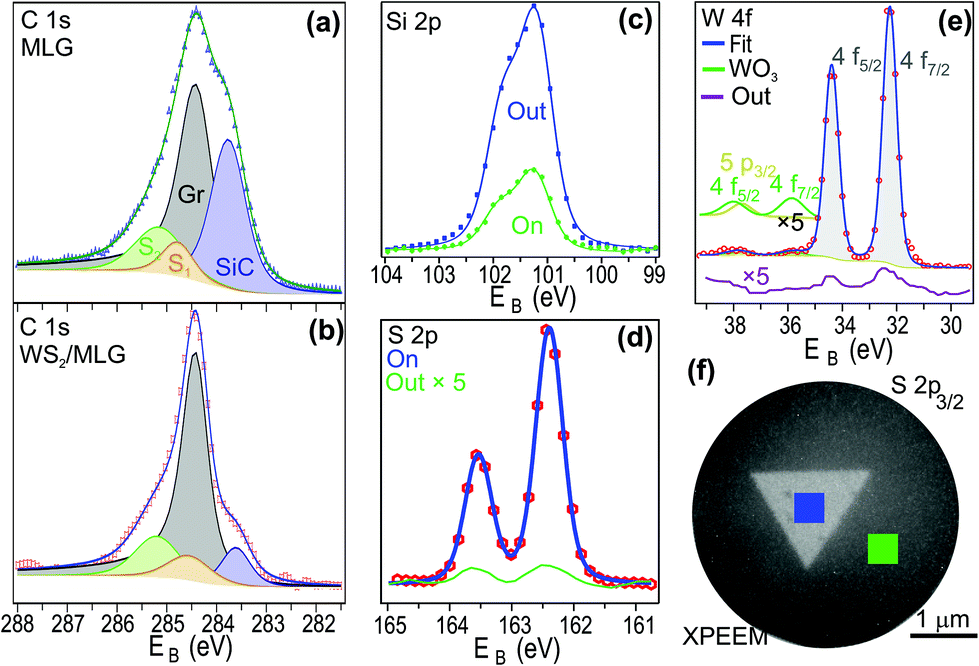 | ||
| Fig. 4 Panels (a–e): Core level photoemission spectroscopy spectra extracted from XPEEM scan at 400 eV. The label “out” indicates that the spectrum was recorded outside the triangle. (f) XPEEM snapshot of S 2p extracted on the high-spin component highlighting the areas from which the spectra are extracted. The same areas are valid for the W 4f spectra. | ||
In Fig. 4(a) and (b) we compare the C 1s spectra recorded on MLG and WS2/MLG, respectively. Intensities are area normalized so that line-shape and peak positions can be better compared. We point out that, within the experimental error, the positions of the C 1s components do not shift. In particular, the sp2 graphitic peak remains at 284.4 ± 0.1 eV, confirming the absence of doping variation in graphene (cf. section 3.2) and at the same time excluding strong chemical interaction between the two 2D layers. Because their shape is not explicitly evident at this particular photon energy, the S1 and S2 components – characterizing the buffer layer – were assigned from literature data.27 We find S1 at 284.7 ± 0.2 eV and S2 at 285.2 ± 0.1 eV. Again, their positions are stable on and outside the WS2 island. The SiC component is found at 283.7 ± 0.1 eV in both cases, meaning that the WS2 layer does not induce any band bending of the SiC core-level bands. Such a fact is further confirmed by the Si 2p peak, shown in Fig. 4(c). Also in that case, the 2p doublet remains at 101.2 ± 0.1 eV. Panels (d) and (e) display the S 2p and W 4f spectra, respectively. The S 2p is well fitted with a single Voigt doublet with Lorentian width 0.09 eV and Gaussian width 0.2 eV, with the 2p3/2 component centered at 262.2 ± 0.1 eV. This is symptomatic of the fact that the sulphur atoms of both top and bottom layers are in the same chemical environment and the interaction with the graphene pz orbitals does not induce a measurable chemical shift. The W 4f contains a visible second component that we ascribe to a high-oxidation state, namely WO3. The intensity of the oxide doublet is about 4.5% of that of the 4f disulfide doublet. The energy position of the WS2 W 4f7/2 component is measured as 32.2 ± 0.1 eV and the spin–orbit splitting 2.15 ± 0.05 eV. As for the other peaks, we measured W 4f and S 2p also outside the WS2 triangle and we report those spectra with intensity multiplied by a factor 5 in the figures. We find some sulphur and tungsten with energies compatible with those of WS2. The WO3 was instead detected only on the island, leading us to the conclusion that some unreacted material is embedded into the WS2 or underneath it. In panel (f) we display the XPEEM snapshot acquired at the S 2p3/2 energy, showing the regions where the spectra in and outside the triangle were acquired from.
4 Conclusions
In this article we investigate the properties of CVD-grown WS2 crystals on epitaxial graphene on SiC(0001) by means of microscopy techniques such as LEEM/PEEM and AFM as well as laterally averaging methods as ARPES and XPS. The set of measurements we carry out converges on defining the WS2/MLG a low-interacting system. Indeed, μLEED does not show moiré-like diffraction spots and neither μARPES nor ARPES show replica bands. DFT calculations support the experimental findings by evidencing the absence of gaps (either due to band anticrossing or to superperiodicity effects), which have instead been recently reported for a similar system, e.g. MoS2/graphene. The analysis of core level data excludes substantial chemical shifts and line-shape modifications such as peak broadening or splitting, further confirming the weak interaction between WS2 and graphene. The band alignment between WS2 and graphene is determined. We find that the position of the MLG Dirac point does not change, behavior observed also for MoS2 on MLG,54 and the Ev of WS2 is located 1.84 eV below EF. This strong downshift of about 830 meV of the VB maximum depends on the substrate and it alters the value of work function for the WS2. The band structure of the system is measured through the entire BZ. We extract the effective masses in, finding mh1 ≃ 0.39me for the low energy band and mh2 ≃ 0.53me for the high energy band. The spin–orbit splitting of the VB at is found to be 462 meV, the highest values reported for this material in its monolayer form. Together with the observed 0° azimuthal alignment of the two crystals, the band structure of the system results to be promising for applications in the realm of opto-, spin- and valleytronics.
Conflicts of interest
There are no conflicts to declare.Acknowledgements
The research leading to these results has received funding from the European Union's Horizon 2020 research and innovation program under grant agreement No. 696656 – GrapheneCore1. We gratefully acknowledge CINECA for providing HPC resources under the ISCRA-C grants “Quasi free standing graphene monolayer on SiC with H-coverage vacancies: a density functional theory study” (2016–2017), and “Electro-mechanical manipulation of graphene” (2015–2016), and for technical support. This work was partly supported by the German Research Foundation (DFG) in the framework of the Priority Program 1459 Graphene. The authors also thank the PRIN project 20105ZZTSE_003 for financial support. We thank Alberto Morgante for useful discussions.Notes and references
- A. K. Geim and I. V. Grigorieva, Nature, 2013, 499, 419 CrossRef CAS PubMed.
- A. S. Mayorov, R. V. Gorbachev, S. V. Morozov, L. Britnell, R. Jalil, L. A. Ponomarenko, P. Blake, K. S. Novoselov, K. Watanabe, T. Taniguchi and A. K. Geim, Nano Lett., 2011, 11, 2396–2399 CrossRef CAS PubMed.
- L. Banszerus, M. Schmitz, S. Engels, J. Dauber, M. Oellers, F. Haupt, K. Watanabe, T. Taniguchi, B. Beschoten and C. Stampfer, Sci. Adv., 2015, 1, e1500222–e1500222 Search PubMed.
- A. V. Kretinin, Y. Cao, J. S. Tu, G. L. Yu, R. Jalil, K. S. Novoselov, S. J. Haigh, A. Gholinia, A. Mishchenko, M. Lozada, T. Georgiou, C. R. Woods, F. Withers, P. Blake, G. Eda, A. Wirsig, C. Hucho, K. Watanabe, T. Taniguchi, A. K. Geim and R. V. Gorbachev, Nano Lett., 2014, 14, 3270 CrossRef CAS PubMed.
- A. Kuc, N. Zibouche and T. Heine, Phys. Rev. B: Condens. Matter, 2011, 83, 245213 CrossRef.
- W. Zhao, Z. Ghorannevis, L. Chu, M. Toh, C. Kloc, P.-H. Tan and G. Eda, ACS Nano, 2013, 7, 791–797 CrossRef CAS PubMed.
- H. Jiang, J. Phys. Chem. C, 2012, 116, 7664–7671 CAS.
- S. Jo, N. Ubrig, H. Berger, A. B. Kuzmenko and A. F. Morpurgo, Nano Lett., 2014, 14, 2019 CrossRef CAS PubMed.
- A. Chernikov, T. C. Berkelbach, H. M. Hill, A. Rigosi, Y. Li, O. B. Aslan, D. R. Reichman, M. S. Hybertsen and T. F. Heinz, Phys. Rev. Lett., 2014, 113, 076802 CrossRef PubMed.
- M. D. Fraser, S. Hofling and Y. Yamamoto, Nat. Mater., 2016, 15, 1049 CrossRef CAS PubMed.
- H. R. Gutiérrez, N. Perea-López, A. L. Elías, A. Berkdemir, B. Wang, R. Lv, F. López-Urías, V. H. Crespi, H. Terrones and M. Terrones, Nano Lett., 2013, 13, 3447 CrossRef PubMed.
- T. Scrace, Y. Tsai, B. Barman, L. Schweidenback, A. Petrou, G. Kioseoglou, I. Ozfidan, M. Korkusinski and P. Hawrylak, Nat. Nanotechnol., 2015, 10, 603 CrossRef CAS PubMed.
- A. Avsar, J. Y. Tan, T. Taychatanapat, J. Balakrishnan, G. Koon, Y. Yeo, J. Lahiri, A. Carvalho, A. S. Rodin, E. O'Farrell, G. Eda, A. H. Castro Neto and B. Özyilmaz, Nat. Commun., 2014, 5, 4875 CrossRef CAS PubMed.
- A. Rossi, H. Büch, C. D. Rienzo, V. Miseikis, D. Convertino, A. Al-Temimy, V. Voliani, M. Gemmi, V. Piazza and C. Coletti, 2D Mater., 2016, 3, 031013 CrossRef.
- J. He, N. Kumar, M. Z. Bellus, H.-Y. Chiu, D. He, Y. Wang and H. Zhao, Nat. Commun., 2014, 5, 5622 CrossRef CAS PubMed.
- S. Omar and B. J. van Wees, Phys. Rev. B: Condens. Matter, 2017, 95, 081404 CrossRef.
- H. Tan, Y. Fan, Y. Zhou, Q. Chen, W. Xu and J. H. Warner, ACS Nano, 2016, 10, 7866–7873 CrossRef CAS PubMed.
- T. Georgiou, R. Jalil, B. D. Belle, L. Britnell, R. V. Gorbachev, S. V. Morozov, Y.-J. Kim, A. Gholinia, S. J. Haigh, O. Makarovsky, L. Eaves, L. A. Ponomarenko, A. K. Geim, K. S. Novoselov and A. Mishchenko, Nat. Nanotechnol., 2013, 8, 100 CrossRef CAS PubMed.
- M. Gmitra and J. Fabian, Phys. Rev. B: Condens. Matter, 2015, 92, 155403 CrossRef.
- E. Bauer, Surface Microscopy with Low Energy Electrons, Springer-Verlag NewYork, 2014 Search PubMed.
- K. V. Emtsev, A. Bostwick, K. Horn, J. Jobst, G. L. Kellog, L. Ley, J. McChesney, T. Ohta, S. A. Reshanov, J. Röhrl, E. Rotenberg, A. Schmid, D. Waldmann, H. B. Weber and T. Seyller, Nat. Mater., 2009, 8, 203 CrossRef CAS PubMed.
- Y. Rong, Y. Fan, A. L. Koh, A. W. Robertson, K. He, S. Wang, H. Tan, R. Sinclair and J. H. Warner, Nanoscale, 2014, 6, 12096 RSC.
- The actual electron energy can be defined by performing a LEEM-IV scan. In particular, the electron energy is defined as the start voltage minus the start voltage of the MEM-LEEM transition. cf.Fig. 3(a).
- T. O. Menteş, G. Zamborlini, A. Sala and A. Locatelli, Beilstein J. Nanotechnol., 2014, 5, 1873 CrossRef PubMed.
- A. Locatelli, L. Aballe, T. O. Menteş, M. Kiskinova and E. Bauer, Surf. Interface Anal., 2006, 38, 1554–1557 CrossRef CAS.
- T. O. Menteş and A. Locatelli, J. Electron Spectrosc. Relat. Phenom., 2012, 185, 323 CrossRef.
- K. V. Emtsev, F. Speck, T. Seyller, L. Ley and J. D. Riley, Phys. Rev. B: Condens. Matter, 2008, 77, 155303 CrossRef.
- C. Riedl, C. Coletti and U. Starke, J. Phys. D: Appl. Phys., 2010, 43, 374009 CrossRef.
- S. Forti and U. Starke, J. Phys. D: Appl. Phys., 2014, 47, 094013 CrossRef.
- P. Giannozzi, S. Baroni, N. Bonini, M. Calandra, R. Car, C. Cavazzoni, D. Ceresoli, G. L. Chiarotti, M. Cococcioni, I. Dabo, A. D. Corso, S. de Gironcoli, S. Fabris, G. Fratesi, R. Gebauer, U. Gerstmann, C. Gougoussis, A. Kokalj, M. Lazzeri, L. Martin-Samos, N. Marzari, F. Mauri, R. Mazzarello, S. Paolini, A. Pasquarello, L. Paulatto, C. Sbraccia, S. Scandolo, G. Sclauzero, A. P. Seitsonen, A. Smogunov, P. Umari and R. M. Wentzcovitch, J. Phys.: Condens. Matter, 2009, 21, 395502 CrossRef PubMed.
- T. Cavallucci and V. Tozzini, J. Phys. Chem. C, 2016, 120, 7670–7677 CAS.
- D. Vanderbilt, Phys. Rev. B: Condens. Matter, 1990, 41, 7892 CrossRef.
- A. M. Rappe, K. M. Rabe, E. Kaxiras and J. Joannopoulos, Phys. Rev. B: Condens. Matter, 1990, 41, 1227 CrossRef.
- J. P. Perdew, A. Ruzsinszky, G. I. Csonka, O. A. Vydrov, G. E. Scuseria, L. A. Constantin, X. Zhou and K. Burke, Phys. Rev. Lett., 2008, 100, 136406 CrossRef PubMed.
- S. Grimme, J. Comput. Chem., 2006, 27, 1787–1799 CrossRef CAS PubMed.
- A. Rossi, S. Piccinin, V. Pellegrini, S. de Gironcoli and V. Tozzini, J. Phys. Chem. C, 2015, 119, 7900–7910 CAS.
- Z. Wang, D.-K. Ki, H. Chen, H. Berger, A. H. MacDonald and A. F. Morpurgo, Nat. Commun., 2015, 6, 8339 CrossRef CAS PubMed.
- M. Dendzik, M. Michiardi, C. Sanders, M. Bianchi, J. A. Miwa, S. S. Grønborg, J. V. Lauritsen, A. Bruix, B. Hammer and P. Hofmann, Phys. Rev. B: Condens. Matter, 2015, 92, 245442 CrossRef.
- D. Pierucci, H. Henck, J. Avila, A. Balan, C. H. Naylor, G. Patriarche, Y. J. Dappe, M. G. Silly, F. Sirotti, A. T. C. Johnson, M. C. Asensio and A. Ouerghi, Nano Lett., 2016, 16, 4054 CrossRef CAS PubMed.
- S. Ulstrup, A. G. Čabo, D. Biswas, J. M. Riley, M. Dendzik, C. E. Sanders, M. Bianchi, C. Cacho, D. Matselyukh, R. T. Chapman, E. Springate, P. D. C. King, J. A. Miwa and P. Hofmann, Phys. Rev. B: Condens. Matter, 2017, 95, 041405(R) CrossRef.
- J. Katoch, S. Ulstrup, R. J. Koch, S. Moser, K. M. McCreary, S. Singh, J. Xu, B. T. Jonker, R. K. Kawakami, A. Bostwick, E. Rotenberg and C. Jozwiak, 2017, ArXiv e-prints.
- H. Yuan, Z. Liu, G. Xu, B. Zhou, S. Wu, D. Dumcenco, K. Yan, Y. Zhang, S.-K. Mo, P. Dudin, V. Kandyba, M. Yablonskikh, A. Barinov, Z. Shen, S. Zhang, Y. Huang, X. Xu, Z. Hussain, H. Y. Hwang, Y. Cui and Y. Chen, Nano Lett., 2016, 16, 4738 CrossRef CAS PubMed.
- H. Hibino, H. Kageshima, F. Maeda, M. Nagase, Y. Kobayashi and H. Yamaguchi, Phys. Rev. B: Condens. Matter, 2008, 77, 075413 CrossRef.
- N. Srivastava, Q. Gao, M. Widom, R. M. Feenstra, S. Nie, K. F. McCarty and I. V. Vlassiouk, Phys. Rev. B: Condens. Matter, 2013, 87, 245414 CrossRef.
- R. Feenstra and M. Widom, Ultramicroscopy, 2013, 130, 101 CrossRef CAS PubMed.
- R. M. Feenstra, N. Srivastava, Q. Gao, M. Widom, B. Diaconescu, T. Ohta, G. L. Kellogg, J. T. Robinson and I. V. Vlassiouk, Phys. Rev. B: Condens. Matter, 2013, 87, 041406 CrossRef.
- J. Ristein, S. Mammadov and T. Seyller, Phys. Rev. Lett., 2012, 108, 246104 CrossRef CAS PubMed.
- S. Kopylov, A. Tzalenchuk, S. Kubatkin and V. I. Fal'ko, Appl. Phys. Lett., 2010, 97, 112109 CrossRef.
- J. M. Riley, W. Meevasana, L. Bawden, M. Asakawa, T. Takayama, T. Eknapakul, T. K. Kim, M. Hoesch, S.-K. Mo, H. Takagi, M. S. Sasagawa, T. Bahramy and P. D. C. King, Nat. Nanotechnol., 2015, 10, 1043 CrossRef CAS PubMed.
- S. Jo, D. Costanzo, H. Berger and A. F. Morpurgo, Nano Lett., 2015, 15, 1197 CrossRef CAS PubMed.
- R. Zhang, I.-L. Tsai, J. Chapman, E. Khestanova, J. Waters and I. V. Grigorieva, Nano Lett., 2016, 16, 629 CrossRef CAS PubMed.
- N. Tombros, C. Jozsa, M. Popinciuc, H. T. Jonkman and B. J. van Wees, Nature, 2007, 448, 571 CrossRef CAS PubMed.
- Q. Wu, L. Shen, Z. Bai, M. Zeng, M. Yang, Z. Huang and Y. P. Feng, Phys. Rev. Appl., 2014, 2, 044008 CrossRef.
- S. Ulstrup, A. G. Čabo, J. A. Miwa, J. M. Riley, S. S. Grønborg, J. C. Johannsen, C. Cacho, O. Alexander, R. T. Chapman, E. Springate, M. Bianchi, M. Dendzik, J. V. Lauritsen, P. D. C. King and P. Hofmann, ACS Nano, 2016, 10, 6315 CrossRef CAS PubMed.
Footnote |
| † Electronic supplementary information (ESI) available. See DOI: 10.1039/C7NR05495E |
| This journal is © The Royal Society of Chemistry 2017 |