
 Open Access Article
 This Open Access Article is licensed under a
 Creative Commons Attribution 3.0 Unported Licence
Real-time atomic scale observation of void formation and anisotropic growth in II–VI semiconducting ribbons†
Xing
Huang
 *a,
Travis
Jones
a,
Hua
Fan
a and
Marc-Georg
Willinger
*b
*a,
Travis
Jones
a,
Hua
Fan
a and
Marc-Georg
Willinger
*b
aDepartment of Inorganic Chemistry, Fritz-Haber Institute of Max-Planck Society, Faradayweg 4-6, 14195, Berlin, Germany. E-mail: xinghuang0214@mail.ipc.ac.cn; xinghuang@fhi-berlin.mpg.de
bDepartment of Colloid Chemistry, Max Planck Institute of Colloids and Interfaces, Research Campus Golm, 14424, Potsdam, Germany. E-mail: willinger@fhi-berlin.mpg.de
First published on 25th July 2017
Abstract
Void formation in semiconductors is generally considered to be deteriorating. However, for some systems, void formation and evolution are beneficial and can be used for the fabrication of novel nanostructures. In either scenario, the understanding of void formation and evolution is of both scientific and technical high importance. Herein, using ZnS ribbons as an example, we report real-time observations of void formation and the kinetics of growth at the nano- and atomic scales upon heating. Direct imaging reveals that voids, created by a focused electron beam in wurtzite (WZ) ribbons, have a rectangular shape elongated along the <0001> direction. The voids are enclosed by low-surface-energy planes including {01−10} and {2−1−10}, with minor contribution from the higher-energy {0001} planes. Driven by thermodynamics to minimize surface energy, the voids grow straight along the [000±1] directions, exhibiting a strong anisotropy. Occasionally, we observe oscillatory kinetics involving periodic void growth and shrinkage, likely due to the fluctuation of the local chemical potential leading to a transitional kinetic state. We also reveal that the morphology and growth kinetics of voids are highly structure-dependent. Real-time observation during void growth through the complex WZ–zinc blende (ZB)–WZ structure shows that the void, with an initial elongated rectangular morphology in the WZ domain, transforms into a different shape, dominated by the {110} surfaces, after migrating to a domain of the ZB structure. However, when the void moves from the ZB to the WZ domain, it transforms back into a rectangular shape followed by fast growth along the [0001] direction. Our experimental results, together with density functional theory (DFT) calculations, provide valuable insights into the mechanistic understanding of void formation and evolution in semiconductors. More importantly, our study may shed light on new pathways for the morphological modulation of nanostructures by utilizing the intrinsic anisotropy of void evolution in WZ semiconductors.
Introduction
Post-growth annealing is an important technique used to modulate and tune the physical properties of semiconductors.1 Thermal treatment becomes operative above reconstruction temperatures, where the diffusion processes of atoms in the crystal lattices set in.2,3 The changes effected by annealing are improving the crystallinity,4 activating dopants,5 healing defects,6 releasing strain,7 and modifying morphology, composition and structure,8–10etc., depending on the nature and state of the semiconductors.Annealing can also lead to unwanted side effects, such as the formation of so called “annealing voids” within the matrix.11 These voids are three-dimensional clusters of vacancies, which evolve through capturing or emitting vacancies on the void surfaces.12,13 In most cases, one would try to suppress void formation because they tend to induce deleterious effects and cause structural failure.13
There are, however, specific cases in which void formation is beneficial and can be used for the fabrication of nanostructures.14 Through the interplay with crystallography, controlled void formation may serve as a means to produce nanostructures with desired morphologies that are usually difficult to achieve by direct bottom-up synthesis.15,16 In our previous work, we realized the direct transformation of bulk II–VI semiconducting crystals into crystallographically oriented nanowire arrays by taking advantage of a process typically seen as devastating.14 Here, the anisotropic growth of voids (or holes) through semiconductor crystals upon thermal annealing led to the desired transformation. However, due to lack of atomic level understanding of void formation and evolution, fine control is still lacking. The atomic process of void-mediated morphological transformation in semiconductors, which can only be captured by real-time imaging at the atomic scale, has so far not been revealed.
Herein, we report in situ transmission electron microscopy (TEM) experiments performed on planar ZnS ribbons. Using atomic-scale imaging, we were able to monitor the kinetics of void evolution upon heating. In addition to the observation of anisotropic void growth, the oscillatory kinetics of void growth and shrinkage, as well as crystallography-governed void morphological transformation, have been revealed.
Materials and methods
ZnS ribbons were synthesized by a H2-assisted thermal evaporation method in a tube furnace. The details of the synthetic process can be found in our previous work.17 SEM images were obtained by using a Hitachi S-4800 scanning electron microscope equipped with a field emission gun. In situ heating experiments were performed inside an aberration-corrected FEI 80-300 transmission electron microscope operated at 300 kV. The TEM samples were prepared by drop casting a few drops of suspensions onto a Micro-Electro-Mechanical System (MEMS)-based heating chip, which was later mounted into a low drift TEM heating holder (DENSsolutions). In situ TEM movies are shown at 7(M1), 5(M2), 10(M3), 7(M4), and 5(M5) frames per second. All the movies were recorded at 600 °C.DFT calculations were performed with the PBE exchange and correlation potential18 using the Quantum ESPRESSO (QE) package19 using the Zn ultrasoft pseudopotential (USPP) from the original QE library and the S USPP from the PS library.20 A kinetic energy (charge density) cutoff of 30 Ry (300 Ry) was employed. Surfaces were modeled as symmetric slabs where the central 2 layers were held fixed during ionic relaxation and periodic images were separated by ca. 15 Å of vacuum. In all the cases, we ensured that the surface energies were converged within 5 meV Å−2 with respect to slab thickness and k-point meshes—up to (16 × 16 × 16) for the WZ unit-cell—while using cold smearing21 with a smearing parameter of 0.001 Ry. The surface energies were computed as:
Results and discussion
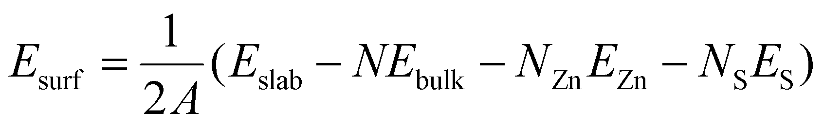
The ZnS ribbons used in our experiments were synthesized by a thermal evaporation method as reported elsewhere by our group.17 The ribbons are about several tens of microns long and 1–7 microns in width, with a typical thickness of about 90–120 nm (Fig. S1†). The TEM overview and the corresponding high-resolution TEM (HRTEM) image in Fig. 1a and b show a ribbon that is oriented along the [0001] direction of the WZ structure. It has a well-defined geometry with rather smooth surfaces, indicating good crystallinity. The marked lattice fringes, with d-spacings of 0.63 and 0.38 nm, correspond to the (0001) and (01−10) planes of the WZ structure. While a majority of the ribbons are purely WZ-structured (Fig. 1a and b), ribbons with structural polymorphism were also observed. Fig. 1c shows an HRTEM image of a ribbon containing both the WZ and ZB phases. Structural analysis reveals that the two phases have an orientation relationship, that is, [0001]WZ//[111]ZB.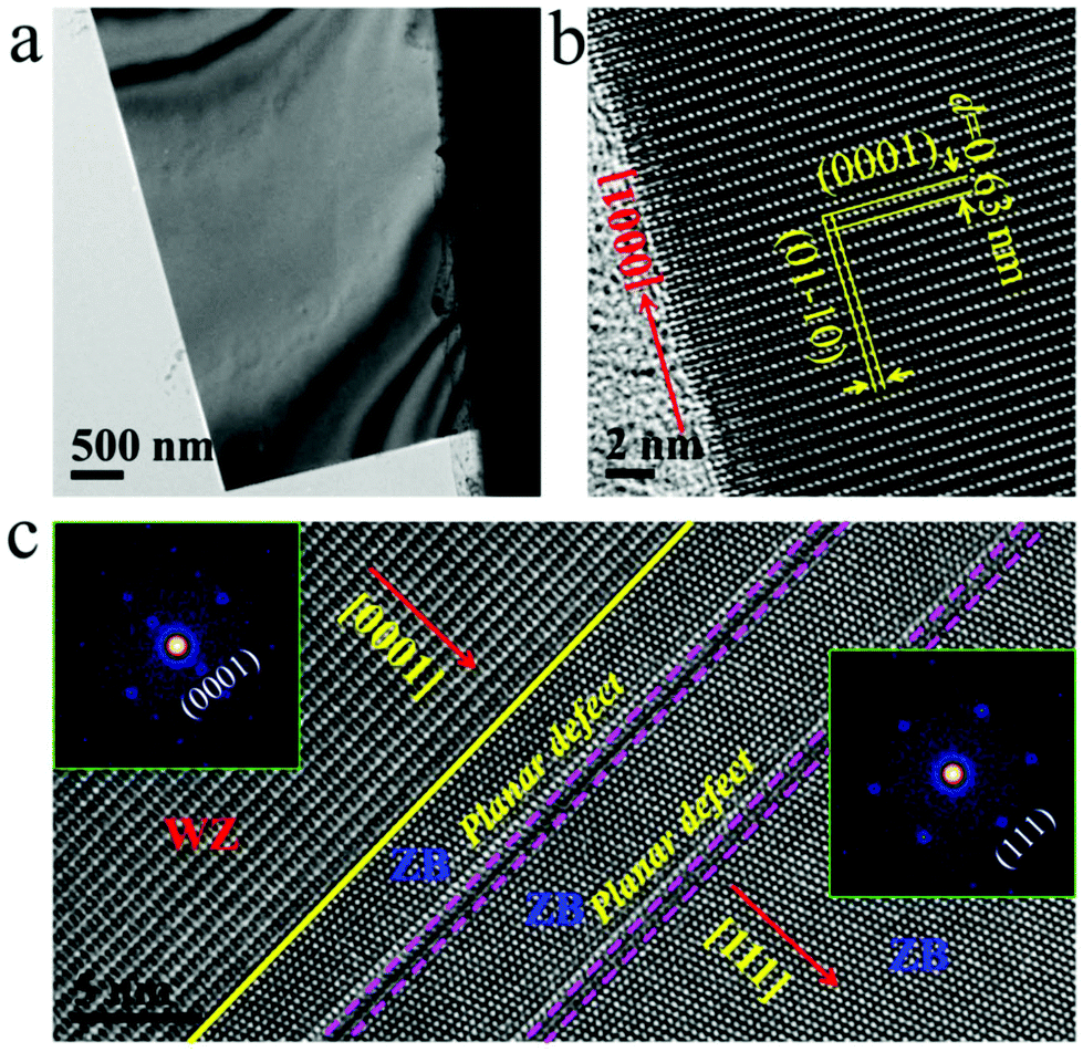 | ||
| Fig. 1 (a) Bright-field TEM image of a planar ZnS ribbon taken at room temperature; (b) HRTEM image of the ZnS ribbon, showing that the ZnS ribbon has a WZ structure and orientates along the [0001] direction; (c) HRTEM image of a ZnS ribbon containing both the ZB and WZ phases. Insets show the fast-Fourier transform (FFT) patterns derived from the WZ ZnS and ZB ZnS segments, respectively. The yellow line indicates the phase boundary of the WZ and ZB segments. The pink dotted lines indicate the planar defect in the ZB structured domain. | ||
In order to investigate the kinetic process of void formation and evolution in ZnS ribbons upon annealing, we performed in situ heating experiments inside the TEM column using a Micro-Electro-Mechanical System (MEMS)-based heating holder (see Fig. 2a). The heating chip (Fig. 2b and c) contains a suspended SiNx ceramic thin membrane with an embedded metallic spiral coil as the heater. The ceramic contains small elongated holes across which the ribbons were suspended for background-free TEM imaging. It was found that the ZnS ribbon remained stable upon heating (at 600 °C) and electron beam irradiation (1.3 × 10⁵ e per nm2 per s); no quantitative variations were observed except for slight carbon contamination on the surface (Fig. S2, ESI†). However, when a focused electron beam was applied on the ZnS ribbon for several seconds during heating (Fig. 2d), significant structural changes occurred (note: during imaging, the electron beam was spread again). A number of well-aligned, rectangular-shaped structures appeared in the region where the ZnS ribbon was pre-irradiated by a focused beam (Fig. 2f). These structures show a very different image contrast compared to the other regions of the ribbon, which was characterized due to the formation of voids (Fig. S3†). Because of the fast kinetics, the void nucleation process was not captured. However, according to previous reports, the stable nuclei are supposed to evolve from the vacancies that were induced by the intense electron beam irradiation.12 Interestingly, the voids did not remain stationary. Instead, anisotropic void growth along one direction was observed (Fig. 2f and Movie M1).
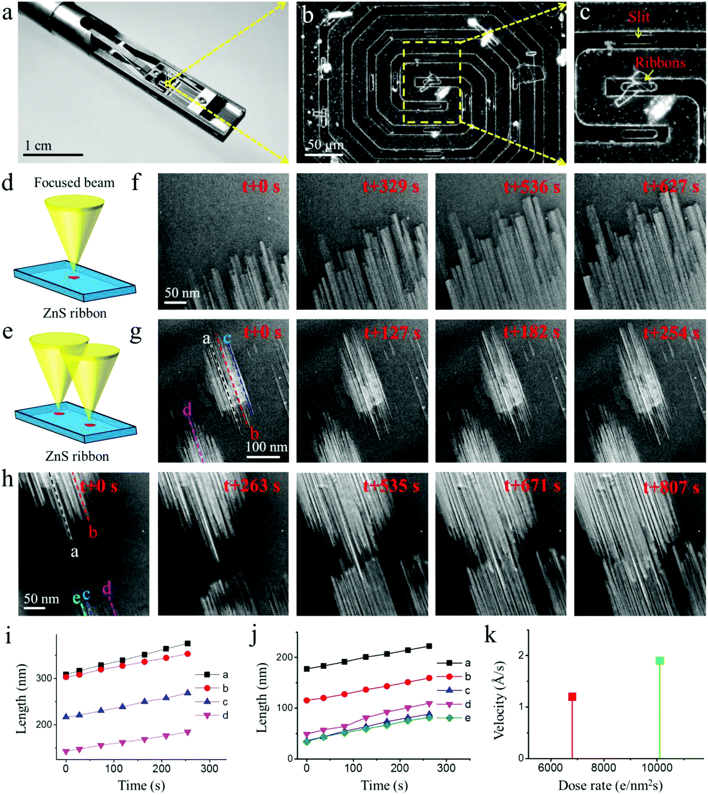 | ||
Fig. 2 (a) Optical images of a TEM heating holder and (b, c) a heating chip loaded with ZnS ribbons; (d, e) schematic drawing to illustrate how structural defects (voids) were created by a focused electron beam; serial TEM images recorded during real-time observation on growth kinetics of one set of voids (f) and different sets of voids (g, h) at 600 °C and at electron dose rates of (f) 10![[thin space (1/6-em)]](https://www.rsc.org/images/entities/char_2009.gif) 700 e per nm2 per s, (g) 6810 e per nm2 per s and (h) 10100 e per nm2 per s; (i, j) growth length of voids as a function of time; the voids used for plotting the diagrams are marked by dotted lines in (g) and (h), respectively; (k) average growth velocity of voids at different electron dose rates. 700 e per nm2 per s, (g) 6810 e per nm2 per s and (h) 10100 e per nm2 per s; (i, j) growth length of voids as a function of time; the voids used for plotting the diagrams are marked by dotted lines in (g) and (h), respectively; (k) average growth velocity of voids at different electron dose rates. | ||
Furthermore, we found that not only the voids in one set, but also the voids in different sets share a common axis in the ribbon (Fig. 2g and h). We sequentially converged the electron beam onto two different spots of the ribbon (Fig. 2e). As such, two sets of voids formed in the ribbon, which was followed by growth along their axes (Movies M2 and 3). Clearly, all the voids of different sets are parallel, irrespective of their locations in the ribbon (Fig. 2g and h). This observation strongly suggests that the observed kinetics relate to the characteristics of the WZ structure. In Fig. 2h, one can observe that the growth of the voids of different sets leads to their intersection (Movie M3). Notably, most of the voids kept growing without interruption, which suggests that the voids locate in different depth positions in the ribbon. Fig. 2i and j show the void length as a function of time. The approximate linear fit suggests that the void growth is a detachment-limited process of the ribbon. In addition, the void growth was found to be influenced by the intensity of the electron beam. The average growth velocity at different electron dose rates is plotted in Fig. 2k. According to the diagram, the growth speed is positively correlated with the electron dose rate. It is probably the case that at a higher electron dose rate more structural defects were induced through knock-on damage and radiolysis,22 which accelerates the kinetic process, thus giving rise to a faster growth speed. Temperature is another parameter that influences the growth. An increased temperature (from 600 to 700 °C) was found to be able to cause a faster growth speed of voids (see Fig. S4†).
Above we have revealed the preferential growth behavior of voids in the ZnS ribbon. However, the growth orientation of voids is still unknown. In order to unveil this information, as well as to learn more about void growth kinetics, an in situ TEM observation during void growth was performed at atomic-resolution. A series of time-sequence HRTEM images are shown in Fig. 3a–c. Although the contrast variation due to the void in the figure is not particularly strong, the intensity profiles (Fig. S5, ESI†) reveal clear variations in the intensity that are sufficient to track the changes in length with time. The marked lattice fringes along the length correspond to the {0001} planes of ZnS, suggesting that the void advanced along the <0001> direction of the WZ structure (Fig. 3a). Structural analysis further reveals that the void is enclosed by the {01−10} and {2−1−10} planes (Fig. 3b and c). The corresponding atomic models for void growth are shown in Fig. 3d–f (plane view) and 3g–i (cross-sectional view), respectively. It should be mentioned that the voids have a plate-like polyhedron shape according to the Wulff construction (Fig. 3j). Due to their elongated geometry, the voids are rich in the {01−10} and {2−1−10} planes, with minor contribution from the {0001} planes. The surface energies of the {01−10} and {2−1−10} planes are much lower than those of the {0001} planes (see Table 1). The voids thus tend to minimize their free energy through this shape. In addition, the growth of the void along the <0001> direction shows a tendency to lower the total surface energy of the system, suggesting that the process is thermodynamically driven.
 | ||
| Fig. 3 (a–c) Serial HRTEM images recorded during void growth along the [0001] direction of the WZ structure at 600 °C and at an electron dose rate of 1.3 × 10⁵ e per nm2 per s; (d–f, g–i) atomic models of void growth viewed along the [2−1−10] and [01−10] projections, respectively; (j) geometry of a void based on the Wulff construction; (k) atomic models of the WZ structure, showing a staking sequence of ABABAB… along the [0001] direction. | ||
| Surface of WZ | Energy/meV Å−2 |
|---|---|
| (0001) Zn terminated | 100 |
| (000−1) S terminated | 107 |
| (01−10) | 23 |
| (2−1−10) | 23 |
WZ ZnS can be described as a number of alternating planes with tetrahedrally coordinated Zn2+ and S2− stacking along the [0001] direction (see Fig. 3k). The oppositely charged ions produce positively charged Zn-terminated (0001) and negatively charged S-terminated (000−1) polar surfaces.23 Owing to the difference in surface free energy, the reactivity of the (0001) and (000−1) planes is different. We accordingly would expect a difference in the speed of void growth along the [000±1] directions in our system. To examine whether this expectation holds true, we selected three voids growing simultaneously along the [0001] and [000−1] directions, and monitored the growth in length as a function of time (Fig. S6, ESI†). Our kinetic study shows that after 254 s the increased lengths towards [000−1] and [0001] are about 31.77 vs. 35.79 nm, 29.26 vs. 23.67 nm, and 25.4 vs. 25.66 nm for voids 1, 2 and 3, respectively. Thus, there is no preference for growth along either the [0001] direction or the [000−1] direction in the current system. The absence of such a preferential growth mode is likely related to the electron beam irradiation that diminishes the reactivity difference originating from the structural polarity. Other factors, such as different local environment (depth position, neighboring condition), can also influence the kinetics of void growth. The observation of diverse growth lengths of voids 1, 2 and 3 may be supportive of this speculation.
In principle, the observed void growth is a process of preferential sublimation on the (0001) and (000−1) facets upon heating and electron beam irradiation. During sublimation, the atoms are detached from the crystal lattice sites and enter the gas phase. As long as the detachment is the dominant process, void growth will be the main kinetic process that we will observe, as these cases shown in Fig. 2 and 3. However, the example in Fig. 4a–g shows not only void growth, but also, more interestingly, void shrinkage as well as switching of these two competition processes (see the Movie M4). Specifically, it was observed that the preformed voids (marked by i, ii and iii), instead of advancing ahead, retreated back along the [000−1] direction (the direction of void retreat is denoted as the [000−1] direction). This observation is indicative of the detachment no longer being the dominant process; its opposite, i.e., attachment, prevailed instead. The source for the refilling of void largely originates from a re-deposition of gas phase atoms. Alternately, surface diffusion can also lead to void shrinkage. In addition, the observation of void shrinkage without changing their width reveals that the nucleation initialized preferentially on the (0001) facet of the void. This is due to the higher surface energy of the (0001) facet that is favorable for void nucleation (Table 1). However, the shrinkage of the void did not last long for void iii. After 72 s, it started to grow along the [0001] direction again. Similar events also occurred for void ii at 82 s. It is interesting to note that, with voids ii and iii both switched to growth mode, void i, however, kept shrinking during this period. Thus, reverse processes occurred in this local area. The voids ii and iii grew for a short time and then shrank once again. The alternation of the voids’ length as a function of time is plotted in the diagram shown in Fig. 4h. The schematic illustration of void oscillatory behavior is shown in Fig. 4i–l. The occurrence of such kinetics is probably due to the fluctuation of the local chemical potential that leads to a transitional kinetic state. As such, both sublimation and regrowth occur spontaneously, giving rise to the phenomenon of void growth and shrinkage.
 | ||
| Fig. 4 (a–g) Real-time TEM observation of the oscillatory kinetics of void shrinkage and growth in WZ structured ZnS at 600 °C and at an electron dose rate of 1.89 × 10⁵ e per nm2 per s; (h) a diagram showing length variation of a void as a function of time; (i–l) schematic illustration of void oscillatory kinetics. | ||
As mentioned above, ZnS can exist in two crystal structures, i.e., WZ and ZB.24 For nanowires or nanoribbons grown from the vapor phase, it is often observed that the WZ and ZB structures coexist in a single nanowire with an orientation relationship.25,26 This is likely due to the structural similarity of WZ and ZB phases, i.e., they both are tetrahedrally coordinated, and the nearest neighbor coordination is the same (see the Fig. S7†). The difference lies in the second nearest neighbor positions within the Zn or S sub-lattice. Along the close packed direction ([0001] for WZ and [111] for ZB), the stacking sequence of the WZ structure is AB, whereas for the ZB structure it becomes ABC, as illustrated in Fig. S7.† The observation of kinetic processes during void evolution in WZ ZnS warrants a comparative study in its structural polymorph, ZB ZnS. In particular, when considering the difference between the WZ and ZB phases, a diverse mode in void evolution is expected. In fact, an in situ ESEM study in our previous work has revealed that heating of the ZB crystal will lead to the formation of low surface energy steps and terraces on the crystal surface.14 However, owing to the low resolution of SEM, the atomic details of the morphological transformation are still missing. To fill this gap in our knowledge, we performed an in situ TEM experiment on ZB structured ZnS under the same conditions as conducted on the WZ ZnS. Instead of using a phase pure ZB ribbon, we selected ribbons where the ZB and WZ phases co-existed (Fig. 1c). The advantage of using such ribbons is that it not only allows the observation of void formation and evolution in ZB ZnS, but also offers an opportunity to study the kinetic process of void evolution in a complex WZ–ZB–WZ structure upon heating.
We first created voids by focusing the electron beam in a WZ domain that is close to a ZB domain. The voids were observed to grow straight along the [0001] direction after their formation, similar to what is shown in Fig. 3. When the void arrived at the ZB domain, its elongated shape transformed into a shape that is enclosed with a pair of newly generated {110} planes and a (111) plane as its basal plane (Fig. 5a and Movie M5). As time passed by, the void became thicker along the projection, leading to the formation of more {110} generations (Fig. 5b). Since the {110} planes have the lowest surface energy compared to those of the {100} and {111} planes in ZB ZnS according to our DFT calculation (see Table 2), dominance of the {110} surfaces suggests that the void configuration in the ZB structure is driven by thermodynamics. The void kept increasing its area in the ZB domain until the tip of the void reached the upper ZB/WZ phase boundary. After that, the void quickly moved into the WZ region with an accompanying shape transformation from a quasi-parallelogram in the ZB structure into an elongated rectangle in the WZ structure (Fig. 5c and Movie M5). It is also noteworthy that the void in the ZB domain accordingly showed a significant morphological change during the transfer (Fig. 5d). It gradually shrank its area through shortening the gap between the {110} planes and finally, it vanished. The whole morphological transformation during void transfer through the WZ–ZB–WZ structure is schematically illustrated in Fig. 5e. On the basis of the above observation, we can conclude that the morphology and evolution behavior of voids are highly structure-dependent, and can be very different among structures. This character may allow one to modulate the void-mediated morphological transformation accordingly for a desired morphology of nanostructures.
 | ||
| Fig. 5 (a–d) Real-time TEM observation of a void's morphological evolution in the ZB and WZ co-existed ZnS ribbon at 600 °C and at an electron dose rate of 1.97 × 10⁵ e per nm2 per s. The morphology of the void is sensitive to the crystal structure. It starts with an elongated rectangular shape in the WZ structure, which transforms into a quasi-parallelogram shape dominated with {110} planes in the ZB structure. When the void moves from the ZB to the WZ structure, it changes back to its original shape, i.e., an elongated rectangular shape; (e) schematic model of a void's morphological transformation in the WZ–ZB–WZ structured domain. | ||
Conclusion
In summary, void formation and evolution in semiconducting ribbons upon heating were directly observed at nano- and atomic scales by in situ TEM for the first time. Real-time observation reveals that the voids, initiated by an irradiation with a focused electron beam, present an elongated rectangular shape (projection view) in the WZ structure with (000±1) as top and bottom surfaces and {01−10} and {2−1−10} as its side surfaces, respectively. The DFT calculations indicate that the morphology of the void resembles the energetic differences in the planes in thermodynamic equilibrium. Driven by thermodynamics to lower the surface energy, the voids grow straight along the <0001> directions from both sides of the voids. Moreover, owing to the fluctuation of the local chemical potential, a transitional state that simultaneously includes void growth and shrinkage is observed. In contrast, voids in the ZB structure show a different morphological evolution pattern. We find that voids in the ZB region are dominated by {110} surfaces. In this region, the morphological evolution of the void is accompanied by the formation of more {110} generations through thickening along the projection. Therefore, the void shape and evolution behavior show high sensitivity with respect to the crystallography of ZnS. Our experimental results, together with ab initio calculations, provide important insights into understanding the mechanism of void-mediated morphological transformations, which is of both scientific and technical importance for developing new techniques for fabricating unique nanostructures.14 Additionally, void formation and anisotropic evolution upon sublimation can be regarded as inverse growth, which opens up new possibilities to study the growth mechanism of crystals.27Acknowledgements
We thank Dr Elena Willinger and Dr Gerardo Algara-Siller for valuable discussions. Open Access funding provided by the Max Planck Society.References
- Y. N. Robert Doering, Handbook of Semiconductor Manufacturing Technology, CRC Press, Second edn, 2007 Search PubMed.
- A. F. W. Willoughby, Rep. Prog. Phys., 1978, 41, 1665–1705 CrossRef CAS.
- G. Tammann, F. Westerhold, B. Garre, E. Kordes and H. Kalsing, Z. Anorg. Allg. Chem., 1925, 149, 21–98 CrossRef CAS.
- S. A. Rutledge, A. A. Farah, J. Dinglasan, D. J. Anderson, A. Das, J. Goh, C. Goh and A. S. Helmy, J. Phys. Chem. C, 2009, 113, 20208–20213 CAS.
- C. Domke, P. Ebert and K. Urban, Phys. Rev. B: Condens. Matter, 1998, 57, 4482–4485 CrossRef CAS.
- N. Moriya, I. Brener, R. Kalish, W. Pfeiffer, M. Deicher, R. Keller, R. Magerle, E. Recknagel, H. Skudlik, T. Wichert and H. Wolf, J. Appl. Phys., 1993, 73, 4248–4256 CrossRef CAS.
- L. Manna, E. C. Scher, L. S. Li and A. P. Alivisatos, J. Am. Chem. Soc., 2002, 124, 7136–7145 CrossRef CAS PubMed.
- L. De Trizio, F. De Donato, A. Casu, A. Genovese, A. Falqui, M. Povia and L. Manna, ACS Nano, 2013, 7, 3997–4005 CrossRef CAS PubMed.
- W. T. Yuan, Y. Wang, H. B. Li, H. L. Wu, Z. Zhang, A. Selloni and C. H. Sun, Nano Lett., 2016, 16, 132–137 CrossRef CAS PubMed.
- A. O. Yalcin, Z. Fan, B. Goris, W.-F. Li, R. S. Koster, C.-M. Fang, A. van Blaaderen, M. Casavola, F. D. Tichelaar, S. Bals, G. Van Tendeloo, T. J. H. Vlugt, D. Vanmaekelbergh, H. W. Zandbergen and M. A. van Huis, Nano Lett., 2014, 14, 3661–3667 CrossRef CAS PubMed.
- J. S. Vermaak and J. Petruzzello, J. Appl. Phys., 1984, 55, 1215–1217 CrossRef CAS.
- Z. Z. Zhang, T. Y. Liu, A. E. Smith, N. V. Medhekar, P. N. H. Nakashima and L. Bourgeois, J. Appl. Crystallogr., 2016, 49, 1459–1470 CAS.
- W. Z. Xu, Y. F. Zhang, G. M. Cheng, W. W. Jian, P. C. Millett, C. C. Koch, S. N. Mathaudhu and Y. T. Zhu, Nat. Commun., 2013, 4, 6 Search PubMed.
- X. Huang, Y. Q. Yu, T. Jones, H. Fan, L. Wang, J. Xia, Z. J. Wang, L. D. Shao, X. M. Meng and M. G. Willinger, Adv. Mater., 2016, 28, 7603–7612 CrossRef CAS PubMed.
- R. Agarwal, D. N. Zakharov, N. M. Krook, W. J. Liu, J. S. Berger, E. A. Stach and R. Agarwal, Nano Lett., 2015, 15, 3303–3308 CrossRef CAS PubMed.
- S. Yoo, S. A. Akbar and K. H. Sandhage, Adv. Mater., 2004, 16, 260–264 CrossRef CAS.
- X. Huang, Y. Q. Yu, J. Xia, H. Fan, L. Wang, M. G. Willinger, X. P. Yang, Y. Jiang, T. R. Zhang and X. M. Meng, Nanoscale, 2015, 7, 5311–5319 RSC.
- J. P. Perdew, K. Burke and M. Ernzerhof, Phys. Rev. Lett., 1996, 77, 3865–3868 CrossRef CAS PubMed.
- P. Giannozzi, S. Baroni, N. Bonini, M. Calandra, R. Car, C. Cavazzoni, D. Ceresoli, G. L. Chiarotti, M. Cococcioni, I. Dabo, A. Dal Corso, S. de Gironcoli, S. Fabris, G. Fratesi, R. Gebauer, U. Gerstmann, C. Gougoussis, A. Kokalj, M. Lazzeri, L. Martin-Samos, N. Marzari, F. Mauri, R. Mazzarello, S. Paolini, A. Pasquarello, L. Paulatto, C. Sbraccia, S. Scandolo, G. Sclauzero, A. P. Seitsonen, A. Smogunov, P. Umari and R. M. Wentzcovitch, J. Phys.: Condens. Matter, 2009, 21, 19 CrossRef PubMed.
- A. Dal Corso, Comput. Mater. Sci., 2014, 95, 337–350 CrossRef CAS.
- N. Marzari, D. Vanderbilt, A. De Vita and M. C. Payne, Phys. Rev. Lett., 1999, 82, 3296–3299 CrossRef CAS.
- R. F. Egerton, P. Li and M. Malac, Micron, 2004, 35, 399–409 CrossRef CAS PubMed.
- X. Y. Meng, H. Xiao, X. H. Wen, W. A. Goddard, S. Li and G. W. Qin, Phys. Chem. Chem. Phys., 2013, 15, 9531–9539 RSC.
- Z. W. Wang, L. L. Daemen, Y. S. Zhao, C. S. Zha, R. T. Downs, X. D. Wang, Z. L. Wang and R. J. Hemley, Nat. Mater., 2005, 4, 922–927 CrossRef CAS PubMed.
- Y. Jiang, X. M. Meng, J. Liu, Z. R. Hong, C. S. Lee and S. T. Lee, Adv. Mater., 2003, 15, 1195–1198 CrossRef CAS.
- Y. F. Hao, G. W. Meng, Z. L. Wang, C. H. Ye and L. D. Zhang, Nano Lett., 2006, 6, 1650–1655 CrossRef CAS PubMed.
- J. Buha, R. Gaspari, A. E. Del Rio Castillo, F. Bonaccorso and L. Manna, Nano Lett., 2016, 16, 4217–4223 CrossRef CAS PubMed.
Footnote |
| † Electronic supplementary information (ESI) available. See DOI: 10.1039/c7nr02231j |
| This journal is © The Royal Society of Chemistry 2017 |