
 Open Access Article
 This Open Access Article is licensed under a
 Creative Commons Attribution 3.0 Unported Licence
Resonant silicon nanoparticles for enhancement of light absorption and photoluminescence from hybrid perovskite films and metasurfaces†
E.
Tiguntseva
a,
A.
Chebykin
a,
A.
Ishteev
ab,
R.
Haroldson
c,
B.
Balachandran
c,
E.
Ushakova
a,
F.
Komissarenko
a,
H.
Wang
c,
V.
Milichko
a,
A.
Tsypkin
a,
D.
Zuev
a,
W.
Hu
c,
S.
Makarov
 *a and
A.
Zakhidov
ac
*a and
A.
Zakhidov
ac
aITMO University, St Petersburg 197101, Russia. E-mail: s.makarov@metalab.ifmo.ru
bNational University of Science and Technology MISiS, Moscow, 119049, Russia
cUniversity of Texas at Dallas, Richardson, Texas 75080, USA
First published on 17th August 2017
Abstract
Recently, hybrid halide perovskites have emerged as one of the most promising types of materials for thin-film photovoltaic and light-emitting devices because of their low-cost and potential for high efficiency. Further boosting their performance without detrimentally increasing the complexity of the architecture is critically important for commercialization. Despite a number of plasmonic nanoparticle based designs having been proposed for solar cell improvement, inherent optical losses of the nanoparticles reduce photoluminescence from perovskites. Here we use low-loss high-refractive-index dielectric (silicon) nanoparticles for improving the optical properties of organo-metallic perovskite (MAPbI3) films and metasurfaces to achieve strong enhancement of photoluminescence as well as useful light absorption. As a result, we observed experimentally a 50% enhancement of photoluminescence intensity from a perovskite layer with silicon nanoparticles and 200% enhancement for a nanoimprinted metasurface with silicon nanoparticles on top. Strong increase in light absorption is also demonstrated and described by theoretical calculations. Since both silicon nanoparticle fabrication/deposition and metasurface nanoimprinting techniques are low-cost, we believe that the developed all-dielectric approach paves the way to novel scalable and highly effective designs of perovskite based metadevices.
1 Introduction
Interest in organic–inorganic perovskites of the methylammonium lead trihalide (MAPbI3) family increased when their conversion efficiency for photovoltaic (PV) devices increased rapidly from 6.5 to 19% in 2012–2015.1 Solution-based perovskite solar cells demonstrated efficiencies of more than 16–18%.2,3 These impressive performances allowed the perovskites to compete with the leading solar materials of the third generation.4 Advances in film formation and optimized perovskite PV architectures have led to a further conversion efficiency increase to 22.1%.5 Moreover, new applications of these hybrid materials have been investigated, including light emitting diodes, optical amplifiers and lasers.6,7Plasmonic enhancement of light harvesting in perovskite based solar cells and photodetectors has been extensively employed during the last few years.8–26 The perovskite solar cells with incorporated plasmonic nanoparticles (NPs) demonstrate improved efficiencies up to 16.3%![[thin space (1/6-em)]](https://www.rsc.org/images/entities/char_2009.gif) 13 as low-cost designs. Gold NPs are also useful for improving the electronic properties in a hole transport layer for perovskite solar cells.14,27 However, plasmon-induced reduction of exciton binding energy8 of hybrid perovskites and high optical losses in the visible spectral region make the plasmonic NPs harmful for photoluminescence (PL).8,28 Parasitic absorption refers to the loss of photoexcited carriers and generated photons in the metal particles that decay via non-radiative channels that produce heat.29 Therefore, increasing of PL from hybrid perovskite films by incorporating resonant NPs is still a challenge.
13 as low-cost designs. Gold NPs are also useful for improving the electronic properties in a hole transport layer for perovskite solar cells.14,27 However, plasmon-induced reduction of exciton binding energy8 of hybrid perovskites and high optical losses in the visible spectral region make the plasmonic NPs harmful for photoluminescence (PL).8,28 Parasitic absorption refers to the loss of photoexcited carriers and generated photons in the metal particles that decay via non-radiative channels that produce heat.29 Therefore, increasing of PL from hybrid perovskite films by incorporating resonant NPs is still a challenge.
In contrast to plasmonics, all-dielectric nanophotonics based on resonant high-index dielectric NPs is a novel paradigm for light enhancement and manipulation at the nanoscale.30,31 Indeed, excitation of Mie type resonances in such NPs results in strong light scattering and near-field enhancement,32 along with low Ohmic losses. The resonant frequency can be controlled by changing the size and shape of the NPs.33 Silicon NPs are a building block for all-dielectric nanophotonics, being a high-index (n > 3) material in the visible and IR ranges, whereas their optical losses are almost negligible as compared with small plasmonic NPs.34 Therefore, silicon based nanoantennas were successfully used for PL enhancement from dyes.35 Even organometallic perovskites can be considered as a material with a high refractive index, which was recently used for the fabrication of perovskite-based metasurfaces by focused ion beam36 and high-throughput nanoimprint37 lithographies, which demonstrate enhanced PL properties. Moreover, nanoimprinted perovskite metasurfaces significantly improve photodetector characteristics.38
The aim of this work is to apply for the first time resonant dielectric NPs to improve the optical properties of hybrid (organo-metallic) perovskite films. In particular, we show that silicon nanoparticles (Si NPs) on the perovskite surface increase PL by more than 30%. Incorporation of Si NPs into a nanoimprinted perovskite metasurface (shown schematically in Fig. 1) leads to 50% PL enhancement, whereas overall enhancement for a metasurface with Si NPs is about 200% as compared with a smooth perovskite film. Additionally, we show significantly improved light absorption in the near-IR range in a perovskite layer with incorporated Si NPs. Since we use cheap and high throughput methods for Si NPs39 and perovskite metasurface37 fabrication, we believe that our findings pave the way for low-cost and highly efficient perovskite based optoelectronic devices.
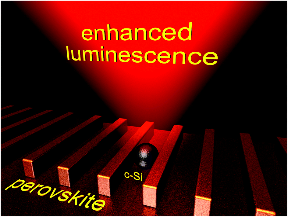 | ||
| Fig. 1 Schematic illustration of luminescence enhancement from a hybrid perovskite metasurface decorated by resonant silicon nanoparticles. | ||
2 Modeling
As shown in the ESI (Fig. S1†), the real part of the refractive index of silicon (n ≈ 3–4) is significantly higher than that of MAPbI3 (n ≈ 2.5) in the visible range. Therefore, optical contrast is enough to excite optical resonances in the silicon sphere even embedded into the perovskite. Our modeling based on Mie theory proves this assumption (see Fig. S2–S4 in the ESI†), revealing the advantage of silicon over widely used titanium dioxide (TiO2 with n ≈ 2.5–2.7) nanoparticles,40,41 where optical contrast with the perovskite is negligibly small.In order to rigorously study the optical properties of Si NPs on top and inside the perovskite film, we carried out numerical simulations using Lumerical FDTD Solutions software. The calculations were performed for the finite computation volume of 5 × 5 × 2 μm surrounded by a perfectly-matched layer (for details, see the ESI†). The thickness of the perovskite film was kept at 800 nm and the radius of randomly distributed Si NPs was varied from R = 25 nm to R = 150 nm to achieve strong resonances in the visible and near-IR ranges (λ = 400–1000 nm). Since the MAPbI3 perovskite has both weaker light absorption and strong PL in the spectral range of 650–950 nm and 770 nm, respectively, we focused our simulations on this range.
First of all, we simulated absorption spectra for the case when NPs were placed on the surface (Fig. 2a). The calculated absorption significantly increases in the spectral range from 650 nm to 950 nm in the case when the NP radius is equal to 100 nm (Fig. 2a). The radius of Si NPs allows for excitation of the first Mie type optical resonance (magnetic dipole resonance, as shown in Fig. S3†) around λ = 750 nm, which requires fulfilling the following conditions in air R ≈ λ/2n, where n is the refractive index of NPs.42 Furthermore, with the increase of NP size, this resonance shifts to the red region, whereas the electric dipole and electric/magnetic quadruple resonances cover the range of λ > 650 nm. Such a broadband resonant behavior can provide near-field enhancement inside the perovskite film and support increased scattering inside the film. Fig. 2b shows the electric field distribution in the sample with Si NPs on the surface. As can be seen from Fig. 2b and Fig. S5,† in the vicinity of the particles, the electric field is enhanced by up to 4.5 times in air, and 3.1 times at the surface underneath as compared with that without the nanoparticles. As a result of the resonance excitation in low-loss Si NPs, there is useful light absorption and field enhancement in the perovskite film.
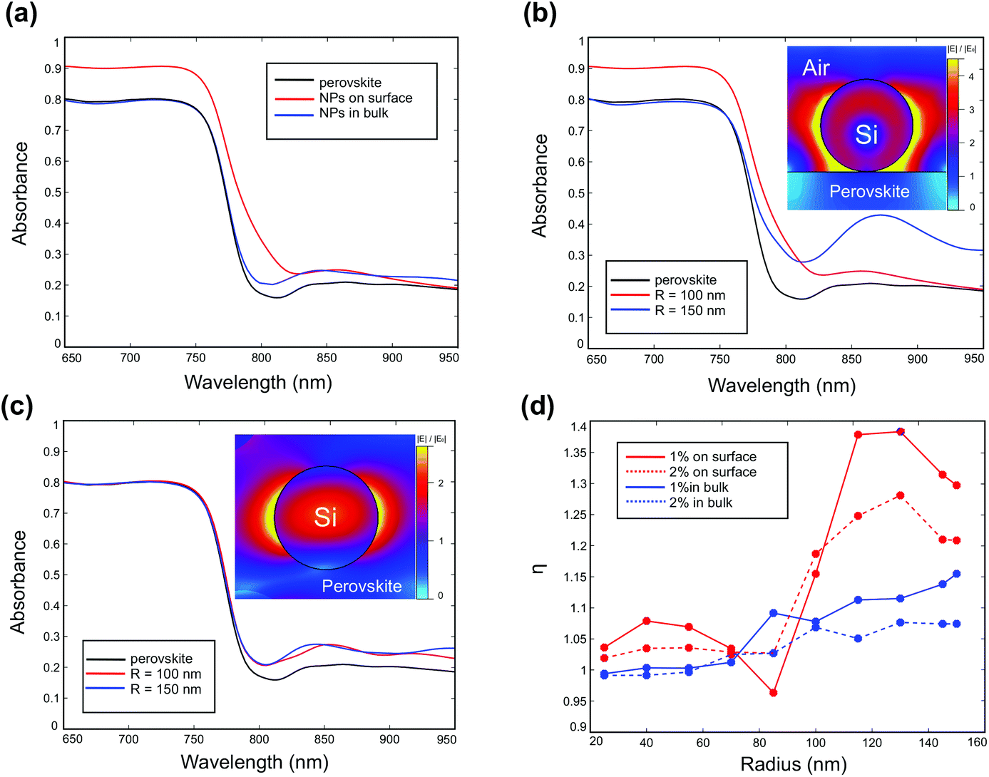 | ||
| Fig. 2 (a) Numerically calculated absorbance spectra for a 800 nm MAIPb3 perovskite film (black line), the same film covered by Si NPs on the surface (red line) and inside the perovskite film (blue line). (b) Modeled absorbance spectra of the perovskite film (black line) with Si NPs on the surface with various radii: 100 nm (red line) and 150 nm (blue line). The inset shows the electrical field distribution at a wavelength of 760 nm for NPs on the surface of the perovskite film. (c) Modeled absorbance spectra of the perovskite film (black line) with embedded Si NPs with radii of 100 nm (red line) and 150 nm (blue line). The inset shows the electrical field distribution at a wavelength of 900 nm for NPs in the bulk of a perovskite film. (d) Dependence of the integral absorption on the Si NP radius (R) at different concentrations of Si NPs: 1% (red solid line) and 2% (red dotted line) on the film surface, and 1% (blue dotted line) and 2% (blue solid line) inside the perovskite film. | ||
The second possibility to increase light absorption and the local electric field in the perovskite layer is to place Si NPs inside the perovskite. In this case, one can expect improved photoexcitation of the perovskite owing to near-field enhancement at resonant conditions. However, owing to reduced optical contrast for the silicon NPs inside the perovskite, the resonances are broadened and overlapped in the optical region (see Fig. S4 in the ESI†). The increase of film absorption is observed only in the range of wavelengths from 780 nm to 950 nm (Fig. 2c). As shown in Fig. 2c, the electric field distributions show field enhancement in the sample with embedded particles in the near-IR range up to 2.5 times, which is similar to the case of TiO2 in air (see Fig. S5†). This fact is also related to the reduction of optical contrast between the Si NPs and surrounding medium, being even more harmful for NPs from materials with a lower refractive index (e.g., TiO2 as shown in the ESI†). When Si NPs are located on the perovskite surface the resonant conditions are not strongly affected by the dielectric substrate,43,44 whereas light confinement and the Mie resonances become much weaker for Si NPs inside the dielectric surrounding medium with a relatively large value of refractive index.
In order to compare the absorption increase in different geometries, it is reasonable to compare the integrals over a broad spectral range (650–950 nm) by using the following formula:
 | (1) |
Fig. 2d shows the dependence of the integral absorption increase from the Si NP radius for two different concentrations of the particles. The highest absorption enhancement is equal to about 39% for the 2% concentration of NPs with a radius of 130 nm deposited on the film surface. At the same time, the embedding or deposition of particles with a radius less or equal to 90 nm makes the integral absorption relatively weaker, i.e. the value of absorbance enhancement varies from 0 to 8%. In the case of the NPs embedded in the perovskite, the maximum of integral absorption (about 17%) is observed for Si NPs with a radius of 150 nm. From our numerical results, one can conclude that the Si NP deposition on the surface of a perovskite film is more effective as compared to NPs embedded in the volume.
3 Experimental results
3.1 Silicon nanoparticles on the perovskite surface
Perovskite films prepared by a solution processing method (for details, see the Experimental section) are investigated by scanning electron microscopy (SEM). The SEM images reveal that the surface consists of non-uniform perovskite grains with an average size around 50–100 nm (Fig. 3a), which is confirmed by our atomic force microscopy measurements (see Fig. S9 in the ESI†). We provide laser printing for crystalline silicon (c-Si) NPs39 on the perovskite surface under specific conditions to obtain more resonant Si NPs for visible and near-IR ranges (for details, see the Experimental section). Based on the SEM images, it is seen that the surface of the perovskite layer is covered by Si NPs randomly. The distribution and sizes of the NPs are studied by SEM. The NP average size varies from 50 to 400 nm, and the size distribution of Si NPs on the surface of the sample is presented in the histogram shown in Fig. 3b.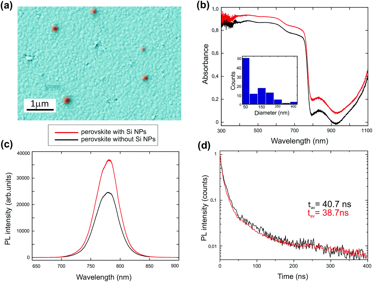 | ||
| Fig. 3 (a) Colored SEM image of a perovskite film with Si NPs on the surface. (b) Absorbance spectra of the perovskite film with (red line) and without (black line) Si NPs. The inset shows the size distribution of the Si NPs in the SEM image. (c) Photoluminescence from perovskites with Si NPs: signal from perovskites with Si NPs (red line), signal from reference perovskites (black line). (d) Time-resolved photoluminescence of perovskites with (red line) and without (black line) Si NPs. | ||
Measurements of the optical properties (reflection and transmission) of the perovskite samples with and without Si NPs show the increase of absorbance values by approximately 0.10–0.20 (Fig. 3b). This correlates with our theoretical analysis (Fig. 2), indicating the important role of the Si NPs for light trapping in their near-field. Indeed, Si NPs with diameters around 150–200 nm possess strong Mie resonances in the spectral range around 700–800 nm (see Fig. 2b).
Excellent near-field enhancement properties of Si NPs can be used not only for absorption enhancement, but also for improving light emission from the perovskite film. Therefore, we study PL resulting from the perovskite covered by Si NPs. The measurements show that the PL signal in the area with Si NPs is stronger than in the area of the sample without nanoparticles (Fig. 3c). Since silicon is an indirect semiconductor, it has a very low quantum efficiency of PL by itself, and generates photons around λ ≈ 1 μm. Therefore, the PL enhancement is mostly attributed to near-field enhancement around the nanoparticles. However, the near-field enhancement is not homogeneous over the film thickness, decaying from top to bottom exponentially. Thus, our value of the PL enhancement of 1.5 is in reasonable agreement with the theoretical estimations.
Time-resolved photoluminescence measurements show almost no changes in the PL decay after Si NP deposition (Fig. 3d), pointing to the absence of any considerable changes in the mobility of photogenerated carriers. This is one of the advantages of laser printing, which does not require any chemical treatment for the perovskite film.
3.2 Silicon nanoparticles embedded inside the perovskite film volume
The laser ablation can be applied not only for Si NP deposition on top of the perovskite layer, but also for embedding them inside the perovskite. For this purpose, several steps have to be performed. Firstly, laser ablation of a single crystalline Si slab in a liquid is provided, generating colloids of spherical crystalline Si NPs with a relatively broad size distribution (for details, see the Experimental section). Toluene is chosen as the host liquid, because it is used during our perovskite film formation and doesn't dissolve the perovskite. The second step is the deposition of the colloids on a liquid layer of a spin-coated perovskite, as shown schematically in Fig. 4. After annealing, the perovskite layer with Si NPs becomes dark and ready for further utilization (for more details of sample preparation, see the Experimental section). As shown in Fig. 5a, Si NPs are distributed randomly inside the perovskite. The average size of the Si NPs is about 140 nm, as shown in Fig. 5b.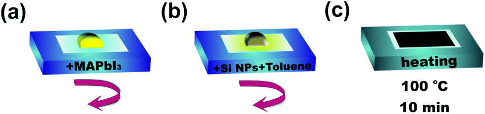 | ||
| Fig. 4 Multistage fabrication of the perovskite film with embedded Si NPs inside. (a) MAPbI3 drop deposition on a substrate by spin-coating. (b) Deposition of Si NP colloids in toluene onto the perovskite film. (c) Heating of the resulting composite film for 10 minutes. | ||
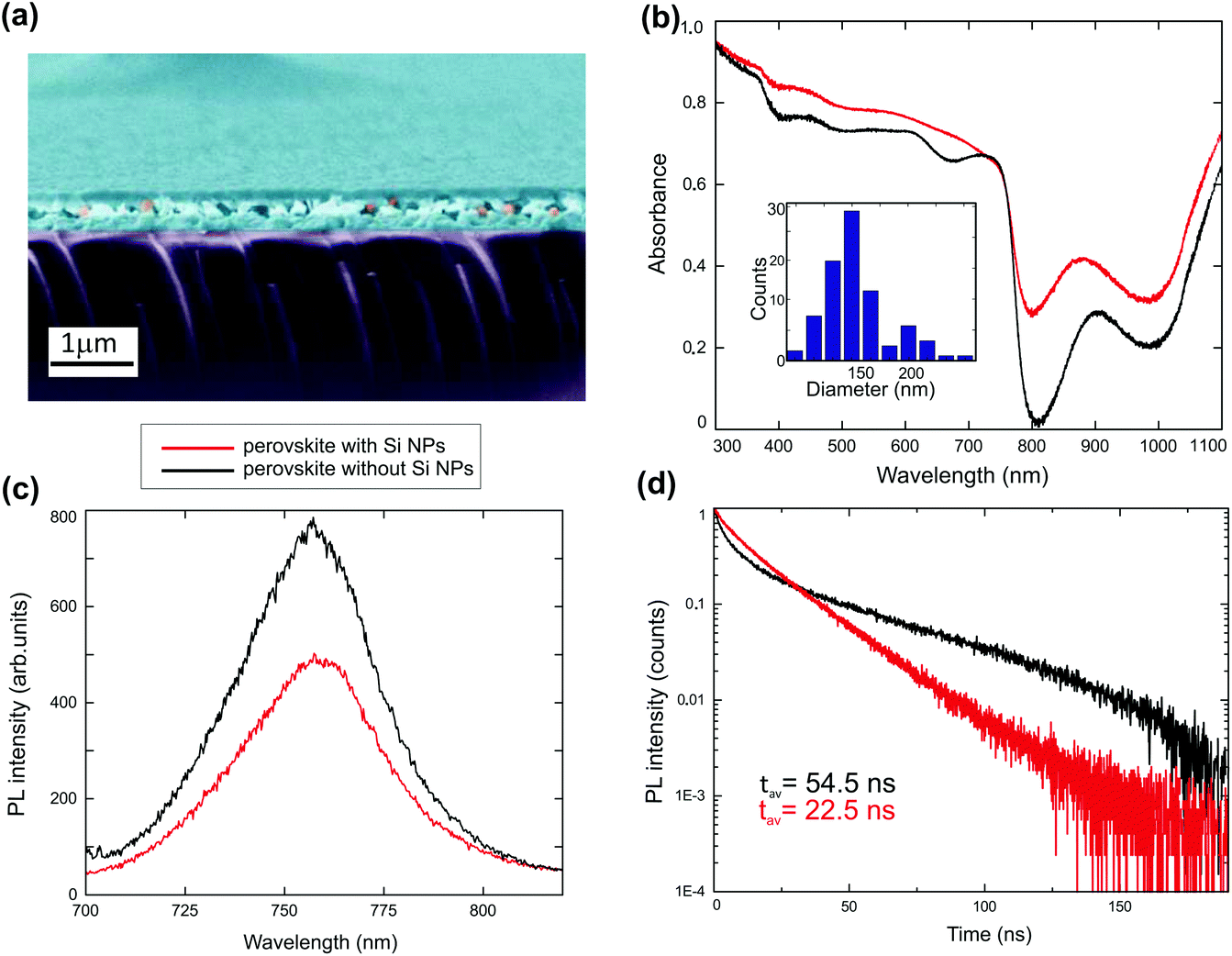 | ||
| Fig. 5 (a) Colored SEM image of a perovskite film cross-section with Si NPs embedded inside. (b) Absorbance spectra of the perovskite film with Si NPs inside (red line) and without (black line). The inset shows the size distribution of the Si NPs inside the hybrid perovskite. (c) Photoluminescence spectra from the perovskite film without (black line) and with (red line) embedded Si NPs inside. (d) Time-resolved photoluminescence of the perovskite film without (black line) and with (red line) embedded Si NPs inside. | ||
In order to characterize the MAPbI3 perovskite layer with embedded Si NPs, we studied its optical properties. According to our reflection/transmission measurements, the absorbance increases from near 0 up to 0.3 at λ ≈ 800 nm (Fig. 5b). However, the PL intensity under 633 nm cw laser photoexcitation is weaker as compared to a similar perovskite without Si NPs (Fig. 5c). Time-resolved PL reveals significant changes in the decay time for the perovskite layer with embedded Si NPs. As a result, embedded Si NPs do not enhance PL but in contrast can even decrease it. This effect can be associated with either local imperfections of the perovskite film or local defect formations, when grains grow around Si NPs of different sizes. Similarly, the dynamics of PL(t) is influenced by such local imperfections at the interface of Si NPs and the volumetrically surrounding grains of the perovskite (Fig. 5d). The Si NPs in this case play the role of additional defects reducing the average PL decay time from 54.5 ns to 22.5 ns, being comparable with previously reported values for perovskite films.45 It is confirmed by fitting the approximation with a biexponential decay law, that Si NPs affect only the slow PL decay component related to radiative recombination, which is sensitive to additional traps and defects (for details of PL decay analysis, see the ESI†).
3.3 Silicon nanoparticles on the perovskite metasurface
Halide perovskite metasurfaces have also been recently used for PL enhancement.36,37 Generally, their enhancement can be even more improved by using resonant Si NPs. Since our previous analysis shows that Si NP laser deposition on top of the perovskite is more preferable for PL enhancement, we provide laser printing for Si NPs on top of the nanoimprinted MAPbI3 metasurface representing periodical stripes with a period of 600 nm, width of 300 nm and height of 350 nm with a 150 nm residual perovskite layer on a thick Si substrate, as shown in Fig. 6a and Fig. S9.† The deposited Si NPs have a similar size distribution as compared with the deposition on smooth surfaces (Fig. 3b) and randomly occupy both maxima and minima of the metasurface grating.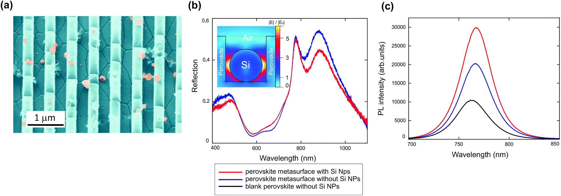 | ||
| Fig. 6 (a) Colored SEM image of the perovskite metasurface with Si NPs. (b) Reflection spectra: signal from the perovskite metasurface (blue line), and perovskite metasurface with Si NPs (red line). The inset shows numerical calculations of near-field around Si NPs on the perovskite metasurface. (c) Photoluminescence modulation by Si-NPs: signal from the blank perovskite (black line), perovskite metasurface (blue line), and perovskite metasurface with Si NPs (red line). | ||
The reflection spectra of the metasurface are shown in Fig. 6b, where the decrease of reflection in the range of 800–1000 nm is observed for the metasurface with deposited Si NPs. The origin of this decrease is related to increased absorption due to the Si NP local field enhancement, as shown in the inset of Fig. 6. Indeed, PL enhancement by 50% as compared with a blank metasurface confirms this assumption (Fig. 6c). Moreover, the total PL enhancement with the metasurface and deposited Si NPs is about 200% (Fig. 6c). Therefore, laser deposition of Si NPs on perovskite surfaces and metasurfaces is a powerful approach to increase their optical properties.
4 Discussion
In previous studies, the incorporation of metal NPs into solar cells increased the enhancement efficiencies through plasmonic effects. The first effect is the near field enhancement of metal NPs upon surface plasmon excitation, enhancing the effective light absorption cross-section of a solar cell.9,46 The second effect is light scattering of the NPs which is employed to re-direct light into an active layer increasing the optical path-length.47 In a third route, metal NPs are utilized as a sensitizer directly to harvest light and inject photo-induced electrons into an electron acceptor.48 Another possible enhancement mechanism is plasmonic heating where the local temperature increase in the metal NPs due to light absorption could result in improved operation of the solar cell.49 Finally, a reduced exciton binding energy, and hence enhanced generation of free charge carriers with the incorporation of the metal NPs is also observed with gold NPs.8In our case, Si NPs likely provide near-field enhancement and light scattering effects, rather than hot electron injection, optical heating or exciton binding energy reduction. Indeed, Si NPs on top of the perovskite significantly enhance absorption, whereas no influence on the PL decay time is observed. Moreover, reduced exciton binding energy gives a lower PL signal at room temperature,8 which is in contradiction with our observation of an enhanced PL signal. As a result, resonant Si NPs demonstrate excellent light harvesting properties as well as an enhanced PL signal without harmful influence of optical losses.
5 Conclusion
We have shown that the novel all-dielectric approach in nanophotonics provides loss-free enhancement of photoluminescence and light harvesting in hybrid perovskites. Our comparative study shows that the direct laser deposition of Si NPs on the perovskite film is preferable for PL and absorption enhancement, which we have used for the enhancement of PL from nanoimprinted perovskite metasurfaces decorated by Si NPs.In contrast to most plasmonic designs, we have observed enhanced photoluminescence owing to reduced non-radiative channels for energy dissipation in the presence of Si NPs, whereas their strong optical resonances increase near-field enhancement and light trapping inside the perovskite layer. The proposed method for the ablative NP integration to nanoimprinted metasurfaces is much cheaper and faster as compared to any lithography techniques. Our results pave the way for novel low-cost hybrid optoelectronic devices based on the concept of all-dielectric NPs combined with perovskite metasurfaces. We believe that our method can be extended to the integration of other resonant dielectric NPs with different band gaps to achieve highly efficient broadband absorption in perovskite solar cells and resonant exciton–exciton interaction50 at the interfaces.
6 Experimental section
6.1 Laser printing
In the laser printing method,39,51 Si NPs are fabricated from a smooth 50 nm a-Si:H film in a single-shot regime and in the forward-transfer geometry, when the receiving substrate is placed under the film with a spacing around 50 μm. This geometry has an advantage over the back-transfer geometry owing to the possibility of NP transfer onto a wide variety of substrates, including opaque and structured samples. The Si NPs are fabricated by means of a Yb3+ femtosecond laser at λ = 1050 nm and at laser energies of E ≈ 50 nJ, focused by a 10× objective (NA = 0.25). The obtained NPs are almost of a spherical shape and their diameters are usually in the range of 50–200 nm, depending on the laser pulse fluence.6.2 Laser ablation in liquids
In order to create pure52 colloids of resonant Si NPs,53 we apply the method of laser ablation in liquids.54 We use a femtosecond laser (Avesta Project) providing laser pulses at λ = 800 nm with an energy up to 2 mJ and a pulse duration of 35 fs at the repetition rate of 1 kHz. Laser pulses are focused by using a lens with a focal length of 10 cm. The sample is placed before the focal plane of the lens.6.3 Perovskite fabrication and incorporation of silicon nanoparticles
A solution of perovskite precursor (MAPbI3) is prepared in a dry-box in the following manner: methylammonium iodide (MAI) in GBL:DMSO with the concentration of 1.2 M is used to dissolve PbI2 (1.2 M). The solution was stirred and heated (70 °C) overnight and used after filtration through a 0.45 μm PTFE syringe filter. Deposition of perovskite layers inside the dry box is performed by using a solvent-engineering technique. Glass substrates are washed by sonication, in deionized water, toluene, acetone, and isopropanol, consecutively. Spin-coating of the MAI + PbI2 solution runs in two steps at 1000 rpm and 5000 rpm. In the middle of the second step, Si NPs in toluene are dripped on top of a rotating substrate (Fig. 4b). Each film is annealed at 100 °C for 10 min (Fig. 4c). The procedure is described in more detail elsewhere.26.4 Nanoimprinting
The Si mold with nanostripes is first treated with 1H,1H,2H,2H-perfluorodecyltrichlorosilane (FDTS) in a N-heptone solvent for 5 min and then cleaned with acetone and blow dried with N2. The molds are then annealed at 100 °C for 20 min. Monolayer FDTS was formed on Si molds which served the anti-adhesive purpose in the nanoimprint process. The Si mold is then placed on the perovskite thin-film coated substrate at different areas in a single process. The imprint represents a multi-step process – 90 seconds at a temperature of 35 °C and a pressure of 2 MPa, 180 seconds at a temperature of 55 °C and a pressure of 4 MPa, 180 seconds at a temperature of 75 °C and a pressure of 6 MPa and 1200 seconds at a temperature of 100 °C and a pressure of 7 MPa. The pressure was kept at 7 MPa while the chamber was cooled down to a temperature of 35 °C. The nanoimprint process is then finished and a perovskite metasurface is formed with negative replication of the Si mold.6.5 Transmittance, reflection, and absorbance
For the measurement of optical transmission (T) and reflection (R) we used normal incidence of linearly polarized light from a halogen lamp (HL-2000 FHSA, Ocean Optics), a commercial spectrometer (Horiba LabRam) with a CCD camera (Andor DU 420A-OE 325). For transmission measurements the excitation and collection objectives are used with NA = 0.95 and NA = 0.7, respectively. For reflection measurement an objective with NA = 0.42 is used. Both in experiment and numerical calculations, absorbance is presented in normalized units, i.e. 1 corresponds to absorption of 100% of incident energy.6.6 Photoluminescence (PL)
Characterization of the photoluminescence (PL) properties of the MAPbI3 sample is performed using a multifunctional experimental setup. The deposited Si NPs are observed using a video camera placed in the image plane of our optical scheme. The volume of the measured signal is determined by the numerical aperture of the collection objective (NA = 0.9) and the confocal pinhole diameter (50 μm).396.7 Time-resolved photoluminescence
Photoluminescence decay at room temperature is investigated by using a laser scanning confocal microscope MicroTime 100 (PicoQuant) equipped with an objective (NA = 0.95) and a picosecond pulsed diode laser head (λ = 405 nm), which implements the method of time-correlated single photon counting. All measurements are performed with laser pulses with a repetition rate of 500 kHz and an intensity of I = 2.85 W cm−2. Some variations of PL decay time from sample to sample is related to slight statistical deviations in the conditions for each film preparation and also related to the inhomogeneity of each film.55Author contributions
E.T., E.U., V.M., D.Z., and S.M. conducted the optical experiments. A.I., R.H., B.B., H.W., W.H. and A.T. fabricated the samples. F.K. and V.M. characterized the samples. A.C. carried out the theoretical analysis. S.M. wrote the paper. A.Z. supervised the project.Acknowledgements
The authors acknowledge Prof. C. Simovski and G. Zograf for fruitful discussions. The work was supported by the Ministry of Education and Science of the Russian Federation (Projects 16.8939.2017/8.9 and 2.2267.2017/4.6), and Russian Foundation for Basic Researches (Projects 17-03-00621 and 16-29-05317). S. V. Makarov acknowledges the ITMO Fellowship Program. A. Z. also appreciates partial support from the Welch Foundation (Grant AT 16-17).References
- M. A. Green, A. Ho-Baillie and H. J. Snaith, Nat. Photonics, 2014, 8, 506–514 CrossRef CAS.
- N. J. Jeon, J. H. Noh, Y. C. Kim, W. S. Yang, S. Ryu and S. I. Seok, Nat. Mater., 2014, 13, 897–903 CrossRef CAS PubMed.
- W. Nie, H. Tsai, R. Asadpour, J.-C. Blancon, A. J. Neukirch, G. Gupta, J. J. Crochet, M. Chhowalla, S. Tretiak and M. A. Alam, et al. , Science, 2015, 347, 522–525 CrossRef CAS PubMed.
- V. A. Milichko, A. S. Shalin, I. S. Mukhin, A. E. Kovrov, A. A. Krasilin, A. V. Vinogradov, P. A. Belov and C. R. Simovski, Phys.–Usp., 2016, 59, 727 CrossRef.
- M. Saliba, T. Matsui, J.-Y. Seo, K. Domanski, J.-P. Correa-Baena, M. K. Nazeeruddin, S. M. Zakeeruddin, W. Tress, A. Abate and A. Hagfeldt, et al. , Energy Environ. Sci., 2016, 9, 1989–1997 CAS.
- B. R. Sutherland and E. H. Sargent, Nat. Photonics, 2016, 10, 295–302 CrossRef CAS.
- H. Lin, L. Zhu, H. Huang, C. J. Reckmeier, C. Liang, A. L. Rogach and W. C. Choy, Nanoscale, 2016, 8, 19846–19852 RSC.
- W. Zhang, M. Saliba, S. D. Stranks, Y. Sun, X. Shi, U. Wiesner and H. J. Snaith, Nano Lett., 2013, 13, 4505–4510 CrossRef CAS PubMed.
- H.-L. Hsu, T.-Y. Juang, C.-P. Chen, C.-M. Hsieh, C.-C. Yang, C.-L. Huang and R.-J. Jeng, Sol. Energy Mater. Sol. Cells, 2015, 140, 224–231 CrossRef CAS.
- S. Carretero-Palacios, M. E. Calvo and H. Míguez, J. Phys. Chem. C, 2015, 119, 18635–18640 CAS.
- M. Qian, M. Li, X.-B. Shi, H. Ma, Z.-K. Wang and L.-S. Liao, J. Mater. Chem. A, 2015, 3, 13533–13539 CAS.
- Z. Yuan, Z. Wu, S. Bai, Z. Xia, W. Xu, T. Song, H. Wu, L. Xu, J. Si and Y. Jin, et al. , Adv. Energy Mater., 2015, 5, 1500038 CrossRef.
- M. Saliba, W. Zhang, V. M. Burlakov, S. D. Stranks, Y. Sun, J. M. Ball, M. B. Johnston, A. Goriely, U. Wiesner and H. J. Snaith, Adv. Funct. Mater., 2015, 25, 5038–5046 CrossRef CAS.
- J.-Y. Wang, F.-C. Hsu, J.-Y. Huang, L. Wang and Y.-F. Chen, ACS Appl. Mater. Interfaces, 2015, 7, 27676–27684 CAS.
- M. Long, Z. Chen, T. Zhang, Y. Xiao, X. Zeng, J. Chen, K. Yan and J. Xu, Nanoscale, 2016, 8, 6290–6299 RSC.
- W. R. Erwin, H. F. Zarick, E. M. Talbert and R. Bardhan, Energy Environ. Sci., 2016, 9, 1577–1601 CAS.
- E. S. Arinze, B. Qiu, G. Nyirjesy and S. M. Thon, ACS Photonics, 2016, 3, 158–173 CrossRef CAS.
- S. S. Mali, C. S. Shim, H. Kim, P. S. Patil and C. K. Hong, Nanoscale, 2016, 8, 2664–2677 RSC.
- L. Yue, B. Yan, M. Attridge and Z. Wang, Sol. Energy, 2016, 124, 143–152 CrossRef CAS.
- S. Carretero-Palacios, A. Jiménez-Solano and H. Míguez, ACS Energy Lett., 2016, 1, 323–331 CrossRef CAS PubMed.
- K. Chan, M. Wright, N. Elumalai, A. Uddin and S. Pillai, Adv. Opt. Mater., 2016 DOI:10.1002/adom.201600698.
- M. Omelyanovich, S. Makarov, V. Milichko and C. Simovski, 2016, arXiv preprint arXiv:1601.06778.
- Z. Sun, L. Aigouy and Z. Chen, Nanoscale, 2016, 8, 7377–7383 RSC.
- K. Kolwas and A. Derkachova, J. Phys. Chem. C, 2017, 121, 4524–4539 CAS.
- G. Kakavelakis, K. Alexaki, E. Stratakis and E. Kymakis, RSC Adv., 2017, 7, 12998–13002 RSC.
- A. E. Shalan, T. Oshikiri, H. Sawayanagi, K. Nakamura, K. Ueno, Q. Sun, H.-P. Wu, E. W.-G. Diau and H. Misawa, Nanoscale, 2017, 9, 1229–1236 RSC.
- D. S. Lee, W. Kim, B. G. Cha, J. Kwon, S. J. Kim, M. Kim, J. Kim, D. H. Wang and J. H. Park, ACS Appl. Mater. Interfaces, 2015, 8, 449–454 Search PubMed.
- J. Cui, C. Chen, J. Han, K. Cao, W. Zhang, Y. Shen and M. Wang, Adv. Sci., 2016, 3, 1500312 CrossRef PubMed.
- H. A. Atwater and A. Polman, Nat. Mater., 2010, 9, 205–213 CrossRef CAS PubMed.
- A. I. Kuznetsov, A. E. Miroshnichenko, M. L. Brongersma, Y. S. Kivshar and B. Luk'yanchuk, Science, 2016, 354, aag2472 CrossRef PubMed.
- S. Jahani and Z. Jacob, Nat. Nanotechnol., 2016, 11, 23–36 CrossRef CAS PubMed.
- R. M. Bakker, D. Permyakov, Y. F. Yu, D. Markovich, R. Paniagua-Domínguez, L. Gonzaga, A. Samusev, Y. Kivshar, B. Lukýanchuk and A. I. Kuznetsov, Nano Lett., 2015, 15, 2137–2142 CrossRef CAS PubMed.
- I. Staude, A. E. Miroshnichenko, M. Decker, N. T. Fofang, S. Liu, E. Gonzales, J. Dominguez, T. S. Luk, D. N. Neshev and I. Brener, et al. , ACS Nano, 2013, 7, 7824–7832 CrossRef CAS PubMed.
- M. Decker and I. Staude, J. Opt., 2016, 18, 103001 CrossRef.
- M. Caldarola, P. Albella, E. Cortés, M. Rahmani, T. Roschuk, G. Grinblat, R. F. Oulton, A. V. Bragas and S. A. Maier, Nat. Commun., 2015, 6, 7915 CrossRef CAS PubMed.
- B. Gholipour, G. Adamo, D. Cortecchia, H. N. Krishnamoorthy, M. Birowosuto, N. I. Zheludev and C. Soci, et al. , Adv. Mater., 2017, 29, 1604268 CrossRef PubMed.
- S. V. Makarov, V. Milichko, E. V. Ushakova, M. Omelyanovich, A. Cerdan Pasaran, R. Haroldson, B. Balachandran, H. Wang, W. Hu and Y. S. Kivshar, et al. , ACS Photonics, 2017, 4, 728–735 CrossRef CAS.
- H. Wang, R. Haroldson, B. Balachandran, A. Zakhidov, S. Sohal, J. Y. Chan, A. Zakhidov and W. Hu, ACS Nano, 2016, 10, 10921–10928 CrossRef CAS PubMed.
- P. Dmitriev, S. Makarov, V. Milichko, I. Mukhin, A. Gudovskikh, A. Sitnikova, A. Samusev, A. Krasnok and P. Belov, Nanoscale, 2016, 8, 5043–5048 RSC.
- L. Etgar, P. Gao, Z. Xue, Q. Peng, A. K. Chandiran, B. Liu, M. K. Nazeeruddin and M. Grätzel, J. Am. Chem. Soc., 2012, 134, 17396–17399 CrossRef CAS PubMed.
- J. Yin, H. Qu, J. Cao, H. Tai, J. Li and N. Zheng, RSC Adv., 2016, 6, 24596–24602 RSC.
- G. Mie, Ann. Phys., 1908, 330, 377–445 CrossRef.
- D. L. Markovich, P. Ginzburg, A. Samusev, P. A. Belov and A. V. Zayats, Opt. Express, 2014, 22, 10693–10702 CrossRef CAS PubMed.
- A. E. Miroshnichenko, A. B. Evlyukhin, Y. S. Kivshar and B. N. Chichkov, ACS Photonics, 2015, 2, 1423–1428 CrossRef CAS.
- M. Saba, M. Cadelano, D. Marongiu, F. Chen, V. Sarritzu, N. Sestu, C. Figus, M. Aresti, R. Piras and A. G. Lehmann, et al. , Nat. Commun., 2014, 5, 5049 CrossRef CAS PubMed.
- M. D. Brown, T. Suteewong, R. S. S. Kumar, V. D'Innocenzo, A. Petrozza, M. M. Lee, U. Wiesner and H. J. Snaith, Nano Lett., 2010, 11, 438–445 CrossRef PubMed.
- K. Catchpole and A. Polman, Opt. Express, 2008, 16, 21793–21800 CrossRef CAS PubMed.
- P. Reineck, G. P. Lee, D. Brick, M. Karg, P. Mulvaney and U. Bach, Adv. Mater., 2012, 24, 4750–4755 CrossRef CAS PubMed.
- W.-L. Liu, F.-C. Lin, Y.-C. Yang, C.-H. Huang, S. Gwo, M. H. Huang and J.-S. Huang, Nanoscale, 2013, 5, 7953–7962 RSC.
- V. Agranovich, Y. N. Gartstein and M. Litinskaya, Chem. Rev., 2011, 111, 5179–5214 CrossRef CAS PubMed.
- U. Zywietz, A. B. Evlyukhin, C. Reinhardt and B. N. Chichkov, Nat. Commun., 2014, 5, 3402 Search PubMed.
- A. Al-Kattan, Y. V. Ryabchikov, T. Baati, V. Chirvony, J. F. Sánchez-Royo, M. Sentis, D. Braguer, V. Y. Timoshenko, M.-A. Estève and A. V. Kabashin, J. Mater. Chem. B, 2016, 4, 7852–7858 RSC.
- J. Yan, P. Liu, Z. Lin, H. Wang, H. Chen, C. Wang and G. Yang, ACS Nano, 2015, 9, 2968–2980 CrossRef CAS PubMed.
- D. Zhang, B. Gökce and S. Barcikowski, Chem. Rev., 2017, 117, 3990–4103 CrossRef CAS PubMed.
- X. Wen, R. Sheng, A. W. Ho-Baillie, A. Benda, S. Woo, Q. Ma, S. Huang and M. A. Green, J. Phys. Chem. Lett., 2014, 5, 3849–3853 CrossRef CAS PubMed.
Footnote |
| † Electronic supplementary information (ESI) available. See DOI: 10.1039/C7NR01631J |
| This journal is © The Royal Society of Chemistry 2017 |