
 Open Access Article
 This Open Access Article is licensed under a
 Creative Commons Attribution 3.0 Unported Licence
Effects of graphene defects on gas sensing properties towards NO2 detection†
Filiberto
Ricciardella
 *a,
Sten
Vollebregt
a,
Tiziana
Polichetti
b,
Mario
Miscuglio
cd,
Brigida
Alfano
be,
Maria L.
Miglietta
b,
Ettore
Massera
b,
Girolamo
Di Francia
b and
Pasqualina M.
Sarro
a
*a,
Sten
Vollebregt
a,
Tiziana
Polichetti
b,
Mario
Miscuglio
cd,
Brigida
Alfano
be,
Maria L.
Miglietta
b,
Ettore
Massera
b,
Girolamo
Di Francia
b and
Pasqualina M.
Sarro
a
aDelft University of Technology, Faculty of Electrical Engineering, Mathematics and Computer Science, Department of Microelectronics, Delft, Feldmannweg 17, 2628 CT Delft, Netherlands. E-mail: filiberto.ricciardella@gmail.com
bENEA – Materials and Devices Basic Research Laboratory, Piazzale Enrico Fermi, 1, I – 80055 Portici (Napoli), Italy
cItalian Institute of Technology, Nanochemistry Department, Via Morego, 30, I-16163 Genova, Italy
dUniversity of Genova, Department of Chemistry and Industrial Chemistry, Via Dodecaneso, 33, I-16146 Genova, Italy
eUniversity of Napoli “Federico II”, Department of Physical Sciences, Via Cinthia, I-80126 Napoli, Italy
First published on 5th April 2017
Abstract
The crystal structure of graphene flakes is expected to significantly affect their sensing properties. Here we report an experimental investigation on the crystalline structure of graphene aimed at exploring the effects on the gas sensing properties. The morphology of graphene, prepared via Chemical Vapor Deposition (CVD), Liquid Phase Exfoliation (LPE) and Mechanical Exfoliation (ME), is inspected through Raman spectroscopy, Atomic Force Microscopy (AFM) and Scanning Electron Microscopy (SEM). CVD and LPE-graphene structures are found to be more defective with respect to ME-graphene. The defects are due to the jagged morphology of the films rather than originating from intrinsic disorder. The flatness of ME-graphene flakes, instead, explains the absence of defects. Chemiresistors based on the three different graphene preparation methods are subsequently exposed to NO2 in the concentration range 0.1–1.5 ppm (parts per million). The device performance is demonstrated to be strongly and unambiguously affected by the material structure: the less defective the material is, the higher the response rate is. In terms of signal variation, at 1.5 ppm, for instance, ME-graphene shows the highest value (5%) among the three materials. This study, comparing simultaneously graphene and sensors prepared via different routes, provides the first experimental evidence of the role played by the graphene level of defectiveness in the interaction with analytes. Moreover, these findings can pave the path for tailoring the sensor behavior as a function of graphene morphology.
1. Introduction
After the fabrication of the first graphene (Gr)-based device1 in 2004, extensive research efforts have been made towards the large scale growth of the material while maintaining the supreme properties shown by the crystals produced through mechanical exfoliation (ME). Many routes have been explored, encompassing electro-chemical methods, laser ablation, sublimation of Si from crystalline SiC substrates, liquid phase exfoliation (LPE) and chemical vapor deposition (CVD).2 Particularly as far as the CVD and LPE approaches are concerned, the goal to achieve large scale production has progressed significantly, since very large graphene foils up to 80 cm in length, and large volumes of hundreds of liters have been produced through CVD and LPE, respectively.3,4 Even though the quality of such a produced material is notably increasing, it is worth noting that properties shown by ME-Gr remain a sort of “gold standard” in the scientific community. In fact, all the best performances in terms of electrical, thermal and optical properties have been achieved with devices fabricated using ME-Gr.5,6 The differences between ME-Gr and Gr synthesized by the other routes can be mainly explained by the different atomic structures induced during the synthesizing phase. Whereas in the former case the atomic structure is basically monocrystalline and defect-free, in the latter it is polycrystalline and defective, defects being defined as anything that breaks the symmetry of the crystal.7,8 Due to the manufacturing process, some defects are almost inevitable, such as the film edges that are mostly due to the finite sizes of the synthesized sheets. However, the existence of defected structures does not necessarily represent a drawback. It can in fact provide added value, since the Gr electronic, optical, thermal, mechanical and sensing features can be strongly affected by these defects, making it possible to tailor the local properties of Gr and to achieve other functionalities, like in conventional semiconductors.9,10 Particularly, in the gas sensing field, the role of defects has been extensively investigated, both from the theoretical and experimental points of view, as recently reported by Varghese et al.11Ab initio studies have shown that defected Gr is generally much more sensitive compared to pristine Gr12–15 and experimental work confirmed this behavior.16,17 Besides the difference in overall sensitivity, the response time can also be affected as shown by the analyses of Graphene Oxide (GO) and reduced-GO (rGO) based gas sensors, respectively, by Lu et al. and Robinson et al.. Both reports describe faster and slower regimes in the response curve upon gas exposure.18,19 The fast response can be attributed to the molecular adsorption onto binding sites with low energy, such as sp2-bonded carbon, while the slow response is due to the interactions between gaseous molecules and high-energy binding sites such as vacancies, defects, and oxygen functional groups. Also Kumar et al.20 disclosed that cracks and defects introduced in CVD-Gr by strain can have large effects on the sensing performances, owing to the increase of sites for adsorption of the target gas. Also, Norford and coworkers recently disclosed that the 3-dimensional Gr/rGO sensing performance can be enhanced by increasing reactive sites and, particularly, oxygenated functional groups.22,23 Finally, both the simulations and experimental results confirm that in the case of pristine graphene, prepared by ME, external defects induced by a substrate dominate the sensing characteristics.21In this work, we present the first comparative study on Gr synthetized via CVD, LPE and ME aiming at investigating the role played by the Gr crystalline structure on the interaction mechanism with analytes, in particular towards NO2. The outcomes of the Raman investigation, in addition to the Atomic Force Microscopy (AFM) and Scanning Electron Microscopy (SEM) analyses, originally disclose that CVD-Gr and LPE-Gr possess more defect structures compared to ME-Gr. The defects originate from the jagged morphology of the films rather than from intrinsic disorder. From the sensing point of view, a more defected morphology points out the presence of high-energy binding sites whilst a smoother structure consists mostly of low-energy binding sites, prevalently localized on the basal plane. Therefore, through the investigation of the kinetics upon the analyte interaction, we demonstrate that the low level of ME-Gr defectiveness induces a faster interaction with analytes. This conclusion is not only proven on ME-Gr and LPE-Gr displaying the steepest and the least steep slope, respectively, but also supported by the intermediate behavior of CVD-Gr that results to have a structure in between the other two kinds of materials. Consequently, the interaction kinetics is slower with the increasing level of the material defectiveness. Due to the absence of the signal saturation during the gas flow (Fig. 5), we infer that a more appropriate parameter to perform this study can be the signal slope rather than the current variation. The analysis we hereby present has been implemented adopting NO2 as the target gas since it is widely adopted in the gas sensing research field as a standard for oxidant analytes.6 Also, ME-Gr is well known to be sensitive to this analyte24 and in several studies we have uncovered that both LPE-Gr and CVD-Gr are much more sensitive to NO2 compared to other species.25–28
2. Materials and methods
2.1 Graphene preparation
CVD-Gr was grown on a pre-patterned Mo catalyst in an AIXTRON BlackMagic Pro at 1000 °C, using Ar/H2/CH4 as feedstock at a pressure of 25 mbar. On the pre-patterned structure, the sensors based on CVD-Gr were directly fabricated, as explained in the following.LPE-Gr suspension was synthesized by dispersing graphite flakes (product 332461, Sigma-Aldrich) at 1 mg ml−1 in a water/IPA mixture (7![[thin space (1/6-em)]](https://www.rsc.org/images/entities/char_2009.gif) :1 v/v) and sonicating in an ultrasonic bath kept at 30 W for 48 h.40 Next, a purification step to sift thinner flakes from un-exfoliated graphite crystallites was performed by applying a relative centrifugal g-force (RCF) roughly equal to 200g for 45 min. The estimated concentration of the suspension resulted to be 0.2 mg ml−1.
:1 v/v) and sonicating in an ultrasonic bath kept at 30 W for 48 h.40 Next, a purification step to sift thinner flakes from un-exfoliated graphite crystallites was performed by applying a relative centrifugal g-force (RCF) roughly equal to 200g for 45 min. The estimated concentration of the suspension resulted to be 0.2 mg ml−1.
ME-Gr was produced by micromechanical exfoliation of natural graphite blocks and then transferred to Si wafer covered with 90 nm thick thermally grown SiO2.
2.2 Material characterization
Graphene layers prepared via the different routes were firstly characterized by Raman spectroscopy. The spectra were obtained through a Renishaw inVia Reflex spectrometer equipped with a 514 nm laser in the back-scattering configuration. The laser power was maintained at 5 mW to avoid damage and a 50× objective with a numerical aperture of 0.50 was used giving a spot size of about 3 μm. For each kind of preparation technique, a sample area of 100 × 100 μm2 was mapped, acquiring 100 spectra at a space interval of 10 μm.To further examine the CVD-Gr, LPE-Gr and ME-Gr morphology, a NTEGRA AURA atomic force microscope (AFM) was used, operating in tapping mode with an n-doped Si NSG tip, rate 0.60 Hz and 512 lines. Based on the Gr type, different areas were scanned, ranging from 10 μm × 10 μm for CVD-Gr, to 50 μm × 50 μm in the case of ME-Gr and LPE-Gr. The surface topography was also investigated through a Scanning Electron Microscope (SEM) Philips XL50, using a beam acceleration voltage of 15 kV. For the sake of clarity, since SEM analysis could induce damage in the film, the images were acquired on a twin triad of samples.41,42
2.3 Device preparation and characterization
Based on the different kinds of synthesized materials, the devices were accordingly prepared. CVD-Gr was grown on the seed (Mo) deposited on SiO2/Si and the resistors were directly designed on the pre-patterned Mo (Fig. 4a) using the transfer-free process recently reported in our work.27 As far as ME-Gr is concerned, pads in Ti/Au (5 nm/50 nm) were drawn up by e-beam lithography on pre-selected flakes (Fig. 4b). The complete process description is provided in the ESI.† For LPE-Gr, a few microliters of the suspension were drop-cast onto interdigitated Ti/Au electrodes (IDEs) (5 nm/50 nm) evaporated by e-beam on the SiO2 (90 nm)/Si substrate through a shadow mask (Fig. 4c).I–V measurements on such prepared graphene-based resistors were performed in the range [−1, 1] V through a semi-automatic probe-station equipped with an Agilent 4156C semiconductor parameter analyzer.
As a subsequent step, resistors based on CVD-Gr and ME-Gr were bonded on a chip by means of Al wires having a diameter equal to 30 μm in order to perform on those samples sensing measurements, as addressed in the following. The resistor based on LPE-Gr does not need to be bonded since the pad areas of a few mm2 allow directly to lay down the probes for the sensing measurements.
2.4 Gas sensing tests
The sensing tests on the chemi-resistors were carried out in a customized Gas Sensor Characterization System (GSCS) in which the environmental conditions can be mimicked in terms of temperature, pressure and relative humidity (RH), set at (22 ± 2) °C, (1.00 ± 0.05) bar and 50%, respectively. The GSCS consists of a stainless steel chamber (40 cl), placed in a thermostatic box and provided with an electrical grounded connector for bias and conductance measurements. Different gas concentrations are obtained by programmable mass flow controllers (MFCs). During the measurements, sensors are biased at a constant DC voltage equal to 1 V with a Precision Power Supply TTi QL355 T and the conductance values are recorded by using a high resolution picoammeter Keithley 6485.2.5 Test-protocol description
The devices were subjected to the standard protocol consisting of 12 sequential pulses of NO2 at different concentrations ranging from 1.5 down to 0.12 ppm. Each step lasted for 4 min and was preceded and followed by 20 min long baseline and recovery phases, respectively, under a N2 atmosphere. The baseline preceding the first step is set 10 min longer than in the other steps with the aim to permit the further stabilization of the devices in the test chamber.3. Results and discussion
Fig. 1a shows the Raman profiles averaged on 100 spectra that were captured on the samples prepared according to the three techniques, as described in the section Materials and methods. For comparison, the graphite spectrum is also reported (black line). The typical Raman fingerprint for each kind of preparation technique can be observed and then the average profile was adopted as a tool to compare the prepared materials.29,30 Also, independently from the route used for the graphene preparation, the spectra collections reported in the ESI† highlight a sort of slight inhomogeneity on the inspected area of the samples, which can occur on such a large area and justifies once again the average of the captured signals. By comparing the spectrum of graphite (black line) with the CVD-Gr (red line) and LPE-Gr (green line) one, in Fig. 1a, what immediately stands out is the rise of the D peak, at ∼1350 cm−1, and the change of the 2D band shape, located at ∼2700 cm−1. For the ME-Gr spectrum (blue line), instead, the change of the 2D band is equally evident as well as for the other two cases (Fig. 1b), whereas the D peak is almost absent. Since the D peak originates from the breathing mode of the six-atom ring and requires a defect for its activation, a first indication of the defected structure of LPE-Gr and CVD-Gr is noticeable, compared to ME-Gr. Remarkably, the term “defect” has to be considered in the broadest sense of the term.7 In contrast, the 2D band, an overtone of the D-peak, is activated without requiring the presence of defects. In fact, it is always present even when there is no D-peak.27 Analyzing the structure of the 2D band, Raman spectroscopy allows to immediately assess the average number of graphene layers constituting the investigated sample, although to this respect different criteria need to be applied for each kind of technique.31 For instance, the ratio I(2D)/I(G) and the full width at half maximum of 2D (FWHM(2D)) can be useful for CVD-Gr and ME-Gr, whilst the relative intensities of the 2D sub-components (2D1 and 2D2), drawn as gray and pale blue lines, respectively, in Fig. 1b (green profile), can be a relevant parameter for LPE-Gr. In fact, based on the 2D band shape of the LPE-Gr spectrum, which does not consist of a single component like the former ones, a single Lorentzian does not properly fit. Thus, the same criteria cannot be adopted. That being said, from the acquired Raman spectra, the maps of FWHM(2D) were elaborated (see the ESI†), indicating that the most part of the CVD-Gr sample presents the FWHM(2D) value equal to 55 cm−1 and I(2D)/I(G) around 0.9. The ME-Gr sample, instead, shows FWHM(2D) mostly ranging between 28 and 33 cm−1 and I(2D)/I(G) distributed between 1.5 and 3.5, confirming that, in both cases, films are prevalently constituted of a few and multi-layers of graphene (FLG).29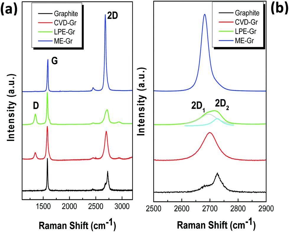 | ||
| Fig. 1 (a) Raman spectra of CVD-Gr (red line), LPE-Gr (green line) and ME-Gr (blue line), respectively, compared to the graphite's profile (black line). Each profile, normalized to the G peak, is determined as the average of 100 spectra captured on areas of 100 × 100 μm2, each at a space interval of 10 μm. (b) Magnification of the 2D band. For LPE-Gr, the 2D band deconvolution allowed to determine the Lorentzian components, 2D1 and 2D2, located at ∼2695 cm−1 and ∼2726 cm−1, respectively. | ||
As far as LPE-Gr is concerned, the 2D band of all spectra is not composed by a single Lorentzian but is generally fitted by the two sub-components. In addition, as shown in Fig. 1b, on average the normalized intensities obey the relation I(2D1) > I(2D2), confirming that also in this case the film can be assumed as composed of FLG.6,26,33,34 Therefore, we can finally infer that, independently from the preparation technique, the three investigated sample surfaces are mostly composed of FLG.
A similar analysis was performed on the D peak, taking into account the ratio I(D)/I(G), especially for CVD-Gr and LPE-Gr, since ME-Gr spectra do not show this feature. In Fig. 2, the map of the I(D)/I(G) ratio, the respective histogram of the ratio distribution and the scatter plot of I(D)/I(G) as a function of FWHM(G) are reported: the panels (a–c) refer to CVD-Gr, and the panels (d–f) correspond to LPE-Gr. As featured by the average spectra (Fig. 1a), in both cases the presence of the D peak is further confirmed over the total mapped surface (panels (a) and (e)). Fig. 2b shows that, in CVD-Gr, the D intensity distribution has a wide dispersion on the mapped area and the most frequently observed value is around 0.2. On the other hand, LPE-Gr is characterized by a sharper distribution of I(D) alongside the sample surface, with the central value at around 0.35. These two almost double values reveal that, although both structures present defects, the sample morphology can also differ between them and surely is quite different from the ME-Gr one, having no D peak. To have a deeper insight, through the scatter plot I(D)/I(G) versus FWHM(G) (Fig. 2c and f) accomplished on the two sets of the collected Raman spectra, the kind of defect characterizing both samples can be evaluated. As stated by Torrisi et al.,32 the lack of correlation in both datasets suggests that the major contribution to the D peak does not originate from intrinsic disorder, but it is more related to the flake structure. As a result, the substantially different structures among the three inspected samples can be finally claimed and further evidence on this respect is delivered by AFM and SEM images (Fig. 3).
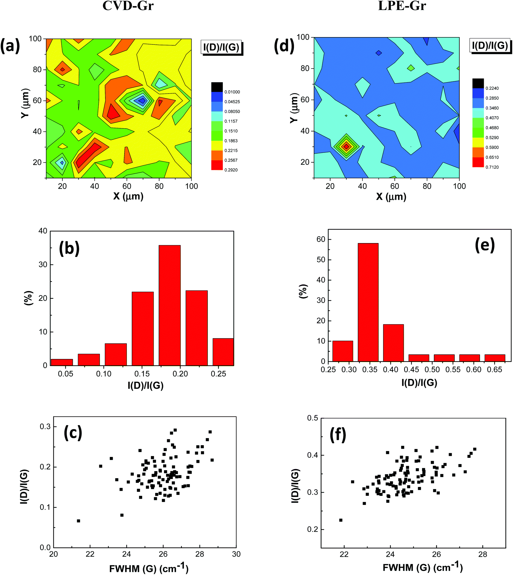 | ||
| Fig. 2 (a) Map of the I(D)/I(G) ratio over the scanned area (100 × 100 μm2) of the CVD-Gr sample. (b) Histogram of the ratio I(D)/I(G) distribution associated with the map in (b). (c) Scatter plot showing the ratio I(D)/I(G) as a function of FWHM(G). Plots and graphs in panels (d–f) refer to LPE-Gr, showing the aforementioned quantities for CVD-Gr. | ||
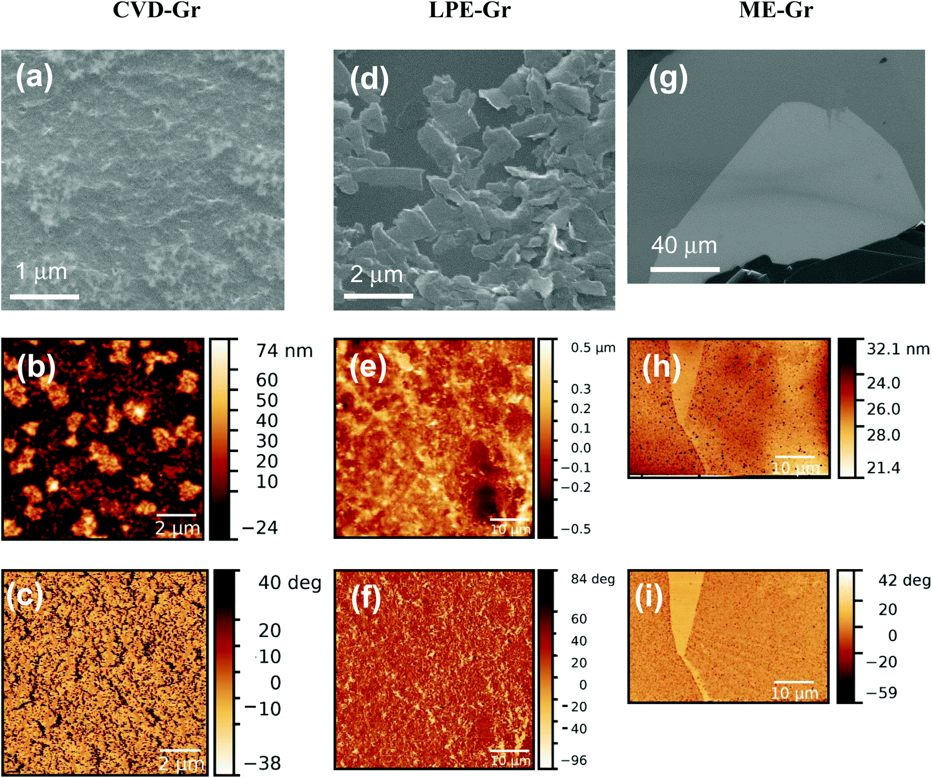 | ||
| Fig. 3 SEM and AFM images of CVD-Gr (panels a–c), LPE-Gr (panels d–f) and ME-Gr (panels g–i). The last two rows show the topography and the phase of the samples, respectively. The scale bar of the SEM images proves that the mean lateral size of ME-Gr flakes is around one order of magnitude higher compared to the LPE-Gr and CVD-Gr one. | ||
Both SEM and AFM analyses (Fig. 3) attest that ME-Gr presents a flat surface having continuous flakes with a mean lateral size in the range of a few tens of microns, as essentially shown by the SEM image (Fig. 3g) and AFM phase (Fig. 3i). As a counterweight, CVD-Gr (Fig. 3a–c) and LPE-Gr (Fig. 3d–f) are mostly composed of flakes with a mean lateral size around one order of magnitude lower, as shown by the scale bars of the SEM images. These findings match the conclusions achieved by means of Raman analysis, especially concerning the D peak. In fact, based on the laser spot size (∼3 μm), the jagged structure of the films acts as the origin of the defects which are indeed due to the flake edges and are totally absent onto the wider surface of ME-Gr. In both cases, i.e. CVD-Gr and LPE-Gr, the rise of these defects is intrinsically associated with the synthesizing routes, since CVD-Gr replicates the catalyst structure35–38 and being the LPE-Gr jagged structure due to the disrupting role played by the ultrasonic waves.39
Once the differences in morphology of the three realized materials were effectively proven, as a next step the sensing properties of such prepared materials were addressed. Devices were realized (see the Materials and methods section) using the Gr sample described in the previous section. The linear behavior of the I–V characteristics (Fig. 4) confirms that ohmic contacts were successfully established between Gr prepared according to the three different approaches and the metal contacts.
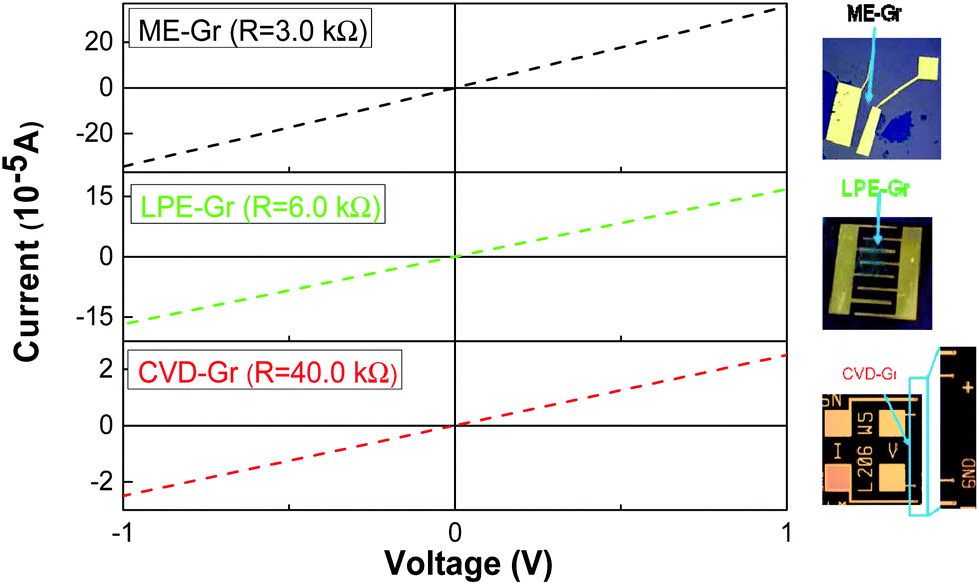 | ||
| Fig. 4 I–V characteristics in the range [−1, +1] V for devices based on CVD-Gr (red curve), LPE-Gr (green curve), ME-Gr (black curve), respectively. For each device, the achievement of the ohmic contact is proven by the linear response. Insets: Pictures of the realized devices. | ||
The devices were rigorously subjected to the same test protocol described in the Experimental section and Fig. 5 shows the dynamic current behavior towards the exposure to NO2. All graphs are normalized to the current value at the gas inlet of the first pulse.
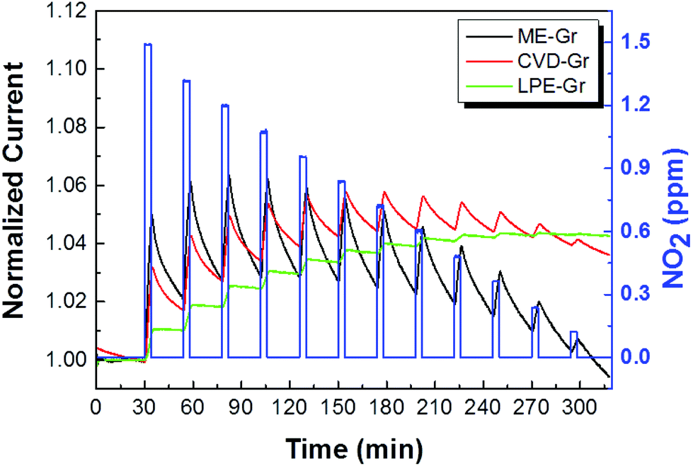 | ||
| Fig. 5 Real-time current behavior of ME-Gr (black line), CVD-Gr (red line) and LPE-Gr (green line) based chemi-resistors upon exposure to sequential NO2 pulses (blue rectangles) at decreasing concentrations from 1.5 down to 0.12 ppm. Each exposure step lasts for 4 min, preceded and followed by 20 min long baseline and recovery phases, respectively, under a N2 atmosphere. The baseline preceding the first pulse lasts for 30 min in order to allow the device to better stabilize in the test chamber. The current is normalized at the value I0 during the gas inlet of the first pulse exposure. | ||
In Fig. 5, a diverse general trend between the three curves is observed. While the graph associated with LPE-Gr (green line) has the tendency to continuously grow and scarcely recover after each single exposure, the opposite can be noticed for ME-Gr (black line). In the last case, the recovery phase is clearly distinguishable after each pulse and the final value of the current is even lower with respect to the beginning of the cycle. CVD-Gr (red line) displays an intermediate behavior between the other two, highlighting a slight recovery phase after the exposure window, even if the overall feature is not comparable to the behavior of the ME-Gr. The argument is further validated by taking into consideration the values of the normalized current at the end of each restoration process. The intermediate behavior of CVD-Gr appears more evident especially at concentrations lower than 0.5 ppm where a slight inversion of this baseline current is highlighted compared to the continuous rise-up related to LPE-Gr and the drastic decrease observed for ME-Gr that is already relevant at around 1 ppm.
These outstanding results denote the first significant proof of concept that the Gr structure can affect the sensing properties, especially bearing in mind that all three films consist of FLG, as previously demonstrated by the Raman analysis.
In an attempt to gain a deeper understanding, the signals during the single beats reported in Fig. 5 were compared, in particular considering the first two steps, where the three curves are mainly overlapping. Fig. 6 shows the magnification of the responses during the first and second gas pulses, at 1.5 and 1.32 ppm, respectively, as indicated in the right y-axis of the panels. During the pulse, a different rising rate for the three devices can be noticed, as further highlighted in the insets of Fig. 6, where the slopes of the current response are enlarged. Also, in Table 1, the fitting values of the slope are compared for both exposure steps and all three devices. It is noteworthy that a clear trend can be remarked: in both cases, ME-Gr shows the fastest rise compared to CVD-Gr and LPE-Gr that, in turn, represents the slowest one. The same was observed for the other gas pulses whose cycles are formed, exploiting the differential method introduced in our previous work (see Fig. S4 in the ESI†).25
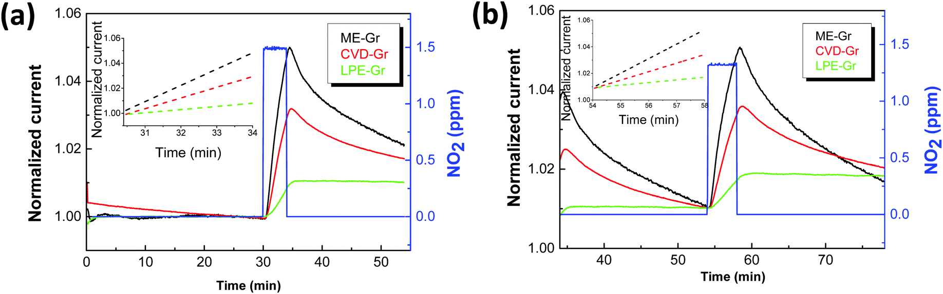 | ||
| Fig. 6 Magnification of the first (a) and second (b) step of the current dynamic response shown in Fig. 5. During the exposure windows towards NO2 (blue rectangles), a different rate of signal growth can be noticed. The curves in panel (b) were shifted to the same starting point in order to facilitate the reader understanding. Insets. Fitting slopes of the rising signal for the three kinds of Gr. A decreasing level of steepness is shown encompassing ME-Gr (black line), CVD-Gr (red line) and LPE-Gr (green line). | ||
| Slope (10−4) | ||
|---|---|---|
| Step 1 (1.5 ppm) | Step 2 (1.32 ppm) | |
| ME-Gr | 2.17 ± 0.04 | 1.82 ± 0.03 |
| CVD-Gr | 1.42 ± 0.01 | 1.07 ± 0.01 |
| LPE-Gr | 0.42 ± 0.01 | 0.33 ± 0.01 |
The key concept relating the Gr structure and the diverse behaviors towards the analyte is tracked down within the context of adsorption sites having high or low binding energy, as reported by Lu et al.18 In that work, similar behaviors to what hereby presented were also addressed as associated with differently structured nano-materials. The authors claimed that diverse regimes and, in turn, different slopes in the response curves during the exposure towards NO2 are due to different interaction mechanisms between the sensing layer and the gas molecules. In particular, fast responses, corresponding to steeper lines, are mainly attributed to sites with low binding energy, such as the sp2-carbon localized on the plane. On the other hand, binding sites having high-energy, such as defects, are responsible for slow responses, i.e. flatter lines.
In this respect, the correspondence between the conclusions achieved in that paper and the experimental data hereby discussed is quite consistent. In fact, ME-Gr, being composed of smooth flakes with a mean lateral size in the range of a few tens of microns, is more prone to provide only low-energy binding sites localized on the surface. In turn, faster responses can be observed, as shown by the response curves in Fig. 6 (black lines). On the opposite, LPE-Gr and CVD-Gr mainly consist of rough flakes having a mean lateral size of a few microns, i.e. an order of magnitude lower compared to ME-Gr. Then, for instance, at a fixed area of the sensing layers prepared according to the three approaches, the flat surface related to ME-Gr is much more predominant than in the other two cases that, instead, are characterized by a higher density of defected structures (Fig. 3a, d and g). As the defects are considered high-energy binding sites, the interaction between molecules and that kind of sites bears out the slower rate of the slopes, as reported in Fig. 6 and Table 1.
Also, despite both LPE-Gr and CVD-Gr exhibiting defected structures (see Raman spectra in Fig. 1), looking at Table 1 and insets of Fig. 6, the slim disparity discerned between them can be explained by considering what has been stated with reference to Fig. 2b and e. The slightly wider diversity of CVD-Gr morphology with respect to the LPE-Gr one can also be interpreted as a simultaneous presence of defected points, as already demonstrated, but also encompassing some zones within the basal plane free of defects.
In other words, on the same sample, not only high-energy binding sites are present, but also sites localized on the plane, indeed low-energy binding sites, are distributed, justifying also the intermediate behavior between ME-Gr and LPE-Gr previously identified (Fig. 5).
4. Conclusions
In summary, a comparative study on Gr prepared via three different approaches, i.e. CVD, LPE and ME, was conducted. The material level of defectiveness was investigated with the aim to explore its effect on the Gr sensing properties. Raman spectroscopy allowed uncovering of the fact that CVD-Gr and LPE-Gr were more defective than ME-Gr, with the defects originating not from intrinsic disorder, but rather from the jagged structure of the material. SEM and AFM analyses attested that the origin of CVD-Gr and LPE-Gr defects relies not only on the flake mean lateral size but also on the film roughness. For both CVD-Gr and LPE-Gr, the rise of these defects is inherent to the synthesizing way. By cross-checking SEM and AFM analyses with the Raman results, ME-Gr did not show any defects owing to both the flat surface and flakes having the mean lateral size in the range of a few tens of microns.The behavior of chemi-resistors based on differently prepared materials towards NO2 was inspected. The experimental data attested a clear correlation between the flake structure and the behavior towards the analyte. ME-Gr showed a faster response rate during the exposure time towards the gas. On the contrary, CVD-Gr and LPE-Gr resulted to have a slower response. The CVD-Gr intermediate behavior between ME-Gr and LPE-Gr is explained by the fact that CVD-Gr consists of a diversified structure. Low-energy binding sites localized on the plane and responsible for the fast regime are present, similarly to ME-Gr. At the same time, as occurs for LPE-Gr, high-energy binding sites, such as defected points, exist, determining the slow rate.
The remarkable findings hereby addressed and, in general, the correlation between the sensor behavior and the purity level of the material justified the best performances reached by ME-Gr based devices compared to the other two. Furthermore, we demonstrated that CVD-Gr represents a promising route to attain comparable results, especially taking into account the large scale production achievable by CVD compared to the manual fabrication of ME-Gr. Therefore, the outcomes can pave routes of possible applications and research developments in the sensing field, mainly related to the capability of tailoring the device performance based on the flake defectiveness level.
Acknowledgements
The authors acknowledge Anna Valota for the preparation of Mechanical Exfoliated samples, Chiara Schiattarella (Department of Physics “E. Pancini”, University of Napoli “Federico II”) for the helpful support in gas sensing measurements and Luana Mazzarella (Technische Universität Berlin) for the fruitful discussion in revising the manuscript.References
- K. S. Novoselov, A. K. Geim, S. V. Morozov, D. Jiang, Y. Zhang, S. V. Dubonos, I. V. Grigorieva and A. A. Firsov, Science, 2004, 306, 666–669 CrossRef CAS PubMed.
- M. J. Allen, V. C. Tung and R. B. Kaner, Chem. Rev., 2010, 110, 132–145 CrossRef CAS PubMed.
- S. Bae, H. Kim, Y. Lee, X. Xu, J.-S. Park, Y. Zheng, J. Balakrishnan, T. Lei, H. R. Kim, Y. I. Song, Y.-J. Kim, K. S. Kim, B. Özyilmaz, J.-H. Ahn, B. H. Hong and S. Iijima, Nat. Nanotechnol., 2010, 5, 574–578 CrossRef CAS PubMed.
- K. R. Paton, E. Varrla, C. Backes, R. J. Smith, U. Khan, A. O′Neill, C. Boland, M. Lotya, O. M. Istrate, P. King and T. Higgins, Nat. Mater., 2014, 13, 624–630 CrossRef CAS PubMed.
- C. Soldano, A. Mahmood and E. Dujardin, Carbon, 2010, 48, 2127–2150 CrossRef CAS.
- F. Ricciardella, PhD thesis, University of Napoli “Federico II”, 2015.
- A. Eckmann, A. Felten, A. Mishchenko, L. Britnell, R. Krupke, K. S. Novoselov and C. Casiraghi, Nano Lett., 2012, 12, 3925–3930 CrossRef CAS PubMed.
- F. Banhart, J. Kotakoski and A. V. Krasheninnikov, ACS Nano, 2010, 5, 26–41 CrossRef PubMed.
- D. W. Boukhvalov and M. I. Katsnelson, Nano Lett., 2008, 8, 4373–4379 CrossRef CAS PubMed.
- M. A. Pimenta, G. Dresselhaus, M. S. Dresselhaus, L. G. Cancado, A. Jorio and R. Saito, Phys. Chem. Chem. Phys., 2007, 9, 1276–1290 RSC.
- S. S. Varghese, S. Lonkar, K. K. Singh, S. Swaminathan and A. Abdala, Sens. Actuators, B, 2015, 218, 160–183 CrossRef CAS.
- Y.-H. Zhang, Y.-B. Chen, K.-G. Zhou, C.-H. Liu, J. Zeng, H.-L. Zhang and Y. Peng, Nanotechnology, 2009, 20, 185504 CrossRef PubMed.
- O. Leenaerts, B. Partoens and F. M. Peeters, Phys. Rev. B: Condens. Matter, 2008, 77, 125416–125422 CrossRef.
- Y. Jiang, S. Yang, S. Li, W. Liu and Y. Zhao, J. Nanomater., 2015, 5 CAS.
- G. Lee, G. Yang, A. Cho, J. W. Han and J. Kim, Phys. Chem. Chem. Phys., 2016, 18, 14198–14204 RSC.
- A. Salehi-Khojin, D. Estrada, K. Y. Lin, M.-H. Bae, F. Xiong, E. Pop and R. I. Masel, Adv. Mater., 2012, 24, 53–57 CrossRef CAS PubMed.
- A. Cagliani, D. M. A. Mackenzie, L. K. Tschammer, F. Pizzocchero, K. Almdal and P. Bøggild, Nano Res., 2014, 7, 743–754 CrossRef CAS.
- G. Lu, S. Park, K. Yu, R. S. Ruoff, L. E. Ocola, D. Rosenmann and J. Chen, ACS Nano, 2011, 5, 1154–1164 CrossRef CAS PubMed.
- J. T. Robinson, F. K. Perkins, E. S. Snow, Z. Wei and P. E. Sheehan, Reduced Graphene Oxide Molecular Sensors, Nano Lett., 2008, 8, 3137–3140 CrossRef CAS PubMed.
- S. Kumar, S. Kaushik, R. Pratap and S. Raghavan, ACS Appl. Mater. Interfaces, 2015, 7, 2189–2194 CAS.
- B. Kumar, K. Min, M. Bashirzadeh, A. Barati Farimani, M.-H. Bae, D. Estrada, Y. D. Kim, P. Yasaei, Y. D. Park, E. Pop and N. R. Aluru, Nano Lett., 2013, 13, 1962–1968 CrossRef CAS PubMed.
- J. Wu, S. Feng, X. Wei, J. Shen, W. Lu, H. Shi, K. Tao, S. Lu, T. Sun, L. Yu, C. Du, J. Miao and L. K. Norford, Adv. Funct. Mater., 2016, 26, 7462–7469 CrossRef CAS.
- J. Wu, K. Tao, J. Miao and L. K. Norford, ACS Appl. Mater. Interfaces, 2015, 7, 27502–27510 CAS.
- F. Schedin, A. K. Geim, S. V. Morozov, E. W. Hill, P. Blake, M. I. Katsnelson and K. S. Novoselov, Nature, 2007, 6, 652–655 CrossRef CAS PubMed.
- F. Ricciardella, E. Massera, T. Polichetti, M. L. Miglietta and G. Di Francia, Appl. Phys. Lett., 2014, 104, 183502 CrossRef.
- B. Alfano, T. Polichetti, M. Mauriello, M. L. Miglietta, F. Ricciardella, E. Massera and G. Di Francia, Sens. Actuators, B, 2016, 222, 1032–1042 CrossRef CAS.
- S. Vollebregt, B. Alfano, F. Ricciardella, A. J. M. Giesbers, Y. Grachova, H. W. van Zeij, T. Polichetti and P. M. Sarro, Proceedings of IEEE 29th International Conference on Micro Electro Mechanical Systems (MEMS), IEEE, Shanghai, 2016.
- F. Ricciardella, S. Vollebregt, T. Polichetti, B. Alfano, E. Massera and P. M. Sarro, Proceedings of IEEE Sensors Conference 2016, IEEE, Orlando, 2016.
- A. C. Ferrari and D. M. Basko, Nat. Nanotechnol., 2013, 8, 235–246 CrossRef CAS PubMed.
- L. M. Malard, M. A. Pimenta, G. Dresselhaus and M. S. Dresselhaus, Raman Spectroscopy in Graphene, Phys. Rep., 2009, 473, 51–87 CrossRef CAS.
- A. C. Ferrari, J. C. Meyer, V. Scardaci, C. Casiraghi, M. Lazzeri, F. Mauri, S. Piscanec, D. Jiang, K. S. Novoselov, S. Roth and A. K. Geim, Phys. Rev. Lett., 2006, 97, 187401 CrossRef CAS PubMed.
- F. Torrisi, T. Hasan, W. Wu, Z. Sun, A. Lombardo, T. S. Kulmala, G.-W. Hsieh, S. Jung, F. Bonaccorso, P. J. Paul, D. Chu and A. C. Ferrari, ACS Nano, 2012, 6, 2992–3006 CrossRef CAS PubMed.
- P. Cataldi, I. S. Bayer, G. Nanni, A. Athanassiou, F. Bonaccorso, V. Pellegrini, A. E. del Rio Castillo, F. Ricciardella, S. Artyukhin, M. A. Tronche, Y. Gogotsi and R. Cingolani, Carbon, 2016, 109, 331–339 CrossRef CAS.
- C. Backes, K. R. Paton, D. Hanlon, S. Yuan, M. I. Katsnelson, J. Houston, R. J. Smith, D. McCloskey, J. F. Donegan and J. N. Coleman, Nanoscale, 2016, 8, 4311–4323 RSC.
- Y. Zhang, L. Zhang and C. Zhou, Acc. Chem. Res., 2013, 46, 2329–2339 CrossRef CAS PubMed.
- Y. Wu, G. Yu, H. Wang, B. Wang, Z. Chen, Y. Zhang, B. Wang, X. Shi, X. Xie, Z. Jin and X. Liu, Carbon, 2012, 50, 5226–5231 CrossRef CAS.
- J. Li, X.-Y. Wang, X.-R. Liu, Z. Jin, D. Wang and L.-J. Wan, J. Mater. Chem. C, 2015, 3, 3530–3535 RSC.
- X. Li, W. Cai, L. Colombo and R. S. Ruoff, Nano Lett., 2009, 9, 4268–4272 CrossRef CAS PubMed.
- U. Khan, A. O'Neill, M. Lotya, S. De and J. N. Coleman, Small, 2010, 6, 864–871 CrossRef CAS PubMed.
- F. Fedi, M. L. Miglietta, T. Polichetti, F. Ricciardella, E. Massera, D. Ninno and G. Di Francia, Mater. Res. Express, 2015, 2, 035601 CrossRef.
- D. Teweldebrhan and A. A. Balandin, Appl. Phys. Lett., 2009, 94, 013101 CrossRef.
- I. Childres, L. A. Jauregui, M. Foxe, J. Tian, R. Jalilian, I. Jovanovic and Y. P. Chen, Appl. Phys. Lett., 2010, 97, 173109 CrossRef.
Footnote |
| † Electronic supplementary information (ESI) available: Details of Raman characterization of samples addressed in the main text. The E-beam lithography procedure adopted for the ME-Gr based sensor realization. A differential method applied to the dynamic sensor behavior. See DOI: 10.1039/c7nr01120b |
| This journal is © The Royal Society of Chemistry 2017 |