
 Open Access Article
 This Open Access Article is licensed under a
 Creative Commons Attribution 3.0 Unported Licence
Investigation of the metal–insulator transition in NdNiO3 films by site-selective X-ray absorption spectroscopy†
Natalia
Palina
 *ab,
Le
Wang
c,
Sibashisa
Dash
acd,
Xiaojiang
Yu
a,
Mark B. H.
Breese
ae,
Junling
Wang
c and
Andrivo
Rusydi
*abe
*ab,
Le
Wang
c,
Sibashisa
Dash
acd,
Xiaojiang
Yu
a,
Mark B. H.
Breese
ae,
Junling
Wang
c and
Andrivo
Rusydi
*abe
aSingapore Synchrotron Light Source, National University of Singapore, Singapore 117603, Singapore. E-mail: natalie.mueller@nus.edu.sg; phyandri@nus.edu.sg
bNUSNNI-Nanocore, National University of Singapore, Singapore 117411, Singapore
cSchool of Materials Science and Engineering, Nanyang Technological University, Singapore 639798, Singapore
dDepartment of Applied Physics, Waseda University, Shinjuku, Tokyo 169-8555, Japan
eDepartment of Physics, National University of Singapore, Singapore 117542, Singapore
First published on 4th April 2017
Abstract
In this work, multifunctional oxide NdNiO3 (NNO) thin films grown on a SrTiO3 (STO) substrate using pulsed-laser deposition are studied. Temperature dependent resistivity measurements revealed that NNO/STO samples exhibit a sharp thickness dependent metal–insulator transition (MIT) over a range of 150–200 K. It is known that the electronic properties of correlated oxides are extremely complex and sensitive to changes in orbital occupancy. To evaluate the changes in the electronic and/or crystallographic structure responsible for the MIT, a site-selective (O, Ni and Nd) X-ray absorption near edge structure (XANES) analysis is performed above and below the transition temperature. Analysis of XANES spectra suggests that: (i) in NNO films nominally trivalent Ni ions exhibit multiple valency (bond disproportionation), (ii) intermetallic hybridization plays an important role, (iii) the presence of strong O 2p–O 2p hole correlation at low temperature results in the opening of the p–p gap and (iv) the valency of Nd ions matches well with that of Nd3+. For NNO films exhibiting a sharp MIT, Ni 3d electron localization and concurrent existence of Ni 3d8 and Ni 3d8![[L with combining low line]](https://www.rsc.org/images/entities/char_004c_0332.gif) 2 states are responsible for the observed transition. At temperatures below the MIT the O 2p–O 2p hole correlation is strong enough to split the O 2p band stabilizing insulating phase. Temperature and thickness dependent differences observed in the site-selective XANES data are discussed in terms of possible mechanisms for the MIT (negative charge-transfer type).
2 states are responsible for the observed transition. At temperatures below the MIT the O 2p–O 2p hole correlation is strong enough to split the O 2p band stabilizing insulating phase. Temperature and thickness dependent differences observed in the site-selective XANES data are discussed in terms of possible mechanisms for the MIT (negative charge-transfer type).
Introduction
Rare earth (R) nickel perovskites (RNiO3) undergo a first-order metal to insulator transition (MIT) as the temperature decreases.1,2 Bulk NdNiO3 (NNO), for example, exhibits the MIT at ∼200 K.3 Traditionally, the origin of the MIT was strongly linked to structural modifications by the lowering of the symmetry from orthorhombic to monoclinic,4 charge ordering5 and a complex antiferromagnetic state.6 RNiO3 thin films grown on bulk substrates are even more complex systems as their properties are affected by the heterointerface formed, which adds an important new dimension to the description of nickelates. RNiO3 thin films exhibit a wide range of exotic properties that originate from the interplay among charge, spin, orbital and lattice degrees of freedom.7–9 Understanding their physical properties still remains a source of considerable scientific debate. Much attention has been focused on treating the origin of the MIT in terms of charge disproportion, e.g. the presence of nonstoichiometric and unstable Ni3+ ions which can split into Ni(3+δ)+ or Ni(3−δ)+ (structural and electronic changes driven by orbital hybridization and/or bond disproportionation).10,11 Another hypothesis focused on strain engineering (lattice distortion), which has been widely accepted to be a driving mechanism responsible for the presence of charge transfer (CT) between transition-metal 3d electrons and oxygen 2p electrons.12–16 However, the importance of intermetallic charge transfer is usually ignored. This originated from the fact that often 4f electrons are considered to be core electrons (localized). However, for a rare-earth of the 4fn6s2 configuration and trivalent metals (such as NNO), the Nd ions have a unique 4fn−15d1 configuration. Therefore, two types of 4f electrons, localized and hybridized, with the other valence electrons (4f band) can be present in the neodymium nickelate.17 The challenge in the reliable assessment of electronic structure modifications lies in the implementation of an experimental technique that is able to treat simultaneously the strong correlation among transition metal 3d, oxygen 2p and rare-earth 4f electrons.In this work, we focus on the evaluation of the changes in electronic and/or crystallographic structure responsible for the MIT by site-selective (O, Ni and Nd) X-ray absorption near edge structure (XANES) analysis. In general, XANES is an element- and symmetry-selective process with a high surface sensitivity, which makes it suitable for (ultra) thin film analysis. The unique value of site-selective XANES analysis is the possibility of obtaining information on: (i) the electronic configuration of constituting elements, (ii) the coordination geometry between metal and ligand (indirectly) and (iii) the possibility of investigating unknown samples based on a comparison with an accurate set of suitable reference compounds, e.g. the so-called ‘fingerprint’ analysis. Additionally, the XANES signal strongly depends on the electronic overlap between the central and bonding atoms, providing insights on the degree of covalency in the sample. Thus, temperature and thickness dependent analyses of XANES data are able to provide the information needed to understand mechanisms responsible for the MIT in NNO films. Here, we present evidence that the sharp MIT in a tensile-strained NNO film is facilitated by the electronic re-localization. The insulating gap opens between O 2p states (O–O insulating gap), accompanied by charge transfer from Ni 3d to Nd 5d orbitals across the MIT, indicating the presence of intermetallic correlation, which can be seen as d-band narrowing. The strength of XANES analysis has been proved to reveal new phenomena at the heterointerface in the LaAlO3/SrTiO3 system.18
Experimental
Sample preparation
NNO films were deposited on (001)-oriented SrTiO3 (STO) substrates by using pulsed laser deposition (PLD). The growth conditions employed for these samples are similar to previous reports.19,20 The roughness and thickness of NNO films were determined using atomic force microscopy (AFM) and X-ray reflectivity data (refer to ESI Fig. 1 and 2†). NNO films with a thickness of 3 nm, 20 nm and 200 nm were studied in this work.Electrical conductivity measurements
To examine the electrical conductivity of NNO/STO samples, in-plane electrical measurements were carried out using a 14 tesla (T) PPMS (physical properties measurement system, Quantum Design) system at temperatures ranging from 10 to 300 K. A linear four-point geometry with square Pt top electrodes with a diameter of 400 μm × 400 μm and a thickness of ∼40 nm were deposited on the NNO films through a metal shadow mask.X-ray absorption near-edge structure (XANES) measurements
The XANES spectra were collected at the SINS beamline at the Singapore Synchrotron Light Source (SSLS), using spherical gratings in a modified dragon-type monochromator with an overall resolution at the oxygen K-edge of about 0.4 eV.21 For spectra acquisition the photon energy was varied to cover the respective edges of the constituting elements, e.g. the O K-edge, the Ni L32-edge and the Nd M54-edge. All XANES measurements were performed in a UHV chamber with a background pressure of about 2 × 10⁻¹⁰ mbar. To evaluate the changes in electronic and/or crystallographic structure of the NNO films, XANES was performed above (295 K) and below (78 K) the MIT transition temperature. Low temperature was achieved using a liquid-nitrogen flow system. Experimental spectra presented here were recorded ex situ and at an X-ray incident angle of 90° using the total electron yield (TEY) mode. Recorded spectra were normalized to the beam current measured by a gold mesh in front of the sample, to correct for synchrotron intensity decay during spectra acquisition. High surface sensitivity was achieved because of the relatively low kinetic energy of the detected electrons. The effective escape depth, and therefore the information depth of the electron yield XANES, has been estimated to be in the range of 3–5 nm for metals and semiconductors, and 5–10 nm for insulators.22,23 The effective information depth implies that site-selective XANES data provide a reliable account of the electronic and/or crystallographic structure of NNO films and the heterointerface formed between the film and the substrate. Utilisation of liquid-helium flow can enable XANES measurements at lower (7 K) temperature, which may seem more accurate based on the data shown in Fig. 1. Regrettably, a liquid-helium flow system was not available at the time of measurements. We argue that temperature dependent analysis of XANES spectra presented here is adequate and capable of unravelling the unique co-dependency of intermetallic (Ni–Nd) and Ni–O covalency. The novelty of these findings is expected to be more pronounced at lower temperature but this would not contradict the main conclusion of this work.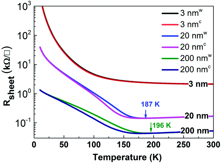 | ||
| Fig. 1 Sheet resistance (Rsheet) versus temperature for NNO films on STO substrates with different thicknesses. The arrows show the metal–insulator transition temperatures on the warming process. Warming and cooling cycle data are marked with superscript “w” and “c”. | ||
Results
Electrical conductivity measurements
Fig. 1 shows the temperature-dependent electrical transport properties of the NNO films. The 200 nm thick NNO film shows clear metallic behaviour at room temperature with a TMI of 196 K, close to the value of bulk NNO. XRD data also verify that the 200 nm NNO film is completely relaxed; therefore, we can consider the 200 nm NNO film to be a representative of bulk NNO.Reducing the film thickness from 200 to 20 nm introduces the strain effect, which lowers TMI to 187 K. In sharp contrast, the 3 nm NNO film grown under the same conditions shows insulator behaviour from room temperature down to 10 K. The sharpness of the MIT shown in Fig. 1 is moderate. The sharpest MIT (3–4 orders of magnitude) is typically observed for NNO films grown on LAO substrates. Here the small lattice mismatch and the sign of strain (e.g. compressive) may be factors explaining the observed discrepancy. For NNO films grown on a STO substrate, the sharpness of the MIT in this work is comparable with the data reported earlier. The small difference in the MIT sharpness can be related to the different methods of NNO film growth, e.g. off-axis radio-frequency magnetron sputtering and pulsed laser deposition.19,20,24
In this work, we focus on the site-selective XANES analysis in order to differentiate driving forces behind the observed MIT as a function of film thickness. In our earlier works, we showed that transport properties as a function of thickness are qualitatively similar for different substrates.19,20 In the present manuscript, we choose the 200 nm NNO film as a representative of bulk NNO because the 200 nm NNO film is completely relaxed. Our efforts were dedicated to the discussion of the strain effect (20 nm thick NNO films) and the dimensionality effect (3 nm thick NNO films) by a thorough investigation of the site-selective XANES data.
O K edge
Fig. 2 shows room-temperature (RT) O K-edge XANES spectra of the 200 nm NdNiO3/SrTiO3 (NNO/STO) sample (as an equivalent to bulk NNO) and NiO and LiNiO2 powders used as a reference for Ni2+ and Ni3+, respectively. Note that for better visualization, the intensity of the XANES spectra for Ni2+ and Ni3+ reference compounds reduced by a factor of 1.6 and 1.2, respectively. For the 200 nm NNO/STO sample, the shape-resonances, indicated as A–G in Fig. 2, arise from the following transitions: (A) a sharp pre-peak at about 528 eV attributed to nickel ions with a formal oxidation state of Ni3+ hybridized with O 2p orbitals. This is evident as the energy position of shape-resonance (A) is consistent with the pre-peak recorded for a Ni3+ reference powder compound (green line in Fig. 2). Additionally, from a spectroscopic point of view, the ground state configuration of Ni3+ ions octahedrally (Oh) coordinated with oxygen is expected to be 3d7. However, due to strong hybridization between Ni 3d and O 2p orbitals, the ground state has considerable 3d8 character, where denotes a ligand hole. The true origin of the shape-resonance observed at 528 eV is assigned to the 3d8 → ![[c with combining low line]](https://www.rsc.org/images/entities/i_char_0063_0332.gif) 3d8 transition, where denotes an O 1s core hole.25–27 It is important to stress that this distinct spectral feature (shape-resonance labelled A) can be considered to be direct spectroscopic evidence of the Ni 3d8 configuration along with holes () on the O 2p valence band. The shoulder-like shape resonances at about 530 eV (B) observed for the NNO/STO XANES spectrum (blue solid line in Fig. 2) originate from the presence of the second crystallographic sites for Ni (e.g. non-equivalent site as compared to A). For more details, refer to the second derivative data shown in ESI Fig. 3,† the area shadowed in light blue and labelled B. Therefore, the main peak at lower energy (528 eV) is characteristic of Ni3+ ions in octahedral (Oh) symmetry, as in NNO bulk. A shoulder at higher energy (530 eV) is attributed to Ni(3−δ)+ ions occupying, for example, square planar (D4h) sites. Splitting is consistent with the data published by other groups.27–29 The broad shape-resonance between 533 eV and 536 eV (C and D) is due to a transition to oxygen 2p states hybridized with Nd (5d, 4f) states.30,31 At high energies, E > 537 eV, shape-resonance features correspond to transitions into hybridized metal–oxygen orbitals involving Ni 4sp/Nd 5sp and O 2p (refer to peaks E, F and G).26,32–34 The energy position of the shape-resonances (E and F) is consistent with those recorded for Ni2+ and Ni3+ reference powder compounds (grey and green spectra in Fig. 2, respectively). For the 200 nm NNO/STO film, the assignment of O K-edge XANES resonance transitions is in good agreement with experimental data of bulk NNO.30,35 Additionally, O K-edge XANES of the reference compounds used in this study is in good agreement with previously reported data.25 Lastly, for Ni2+ and Ni3+ reference compounds, the shape-resonances at about 532 eV (B′) arise from a transition to O 2p orbitals hybridized with Ni2+ (refer to grey Ni2+ reference powder compounds) and the shape-resonance at about 534 eV (C′) is due to Li2O (refer to green Ni3+ reference powder compounds), respectively.25 The latter shape resonance is not present in the NNO/STO samples studied here.
3d8 transition, where denotes an O 1s core hole.25–27 It is important to stress that this distinct spectral feature (shape-resonance labelled A) can be considered to be direct spectroscopic evidence of the Ni 3d8 configuration along with holes () on the O 2p valence band. The shoulder-like shape resonances at about 530 eV (B) observed for the NNO/STO XANES spectrum (blue solid line in Fig. 2) originate from the presence of the second crystallographic sites for Ni (e.g. non-equivalent site as compared to A). For more details, refer to the second derivative data shown in ESI Fig. 3,† the area shadowed in light blue and labelled B. Therefore, the main peak at lower energy (528 eV) is characteristic of Ni3+ ions in octahedral (Oh) symmetry, as in NNO bulk. A shoulder at higher energy (530 eV) is attributed to Ni(3−δ)+ ions occupying, for example, square planar (D4h) sites. Splitting is consistent with the data published by other groups.27–29 The broad shape-resonance between 533 eV and 536 eV (C and D) is due to a transition to oxygen 2p states hybridized with Nd (5d, 4f) states.30,31 At high energies, E > 537 eV, shape-resonance features correspond to transitions into hybridized metal–oxygen orbitals involving Ni 4sp/Nd 5sp and O 2p (refer to peaks E, F and G).26,32–34 The energy position of the shape-resonances (E and F) is consistent with those recorded for Ni2+ and Ni3+ reference powder compounds (grey and green spectra in Fig. 2, respectively). For the 200 nm NNO/STO film, the assignment of O K-edge XANES resonance transitions is in good agreement with experimental data of bulk NNO.30,35 Additionally, O K-edge XANES of the reference compounds used in this study is in good agreement with previously reported data.25 Lastly, for Ni2+ and Ni3+ reference compounds, the shape-resonances at about 532 eV (B′) arise from a transition to O 2p orbitals hybridized with Ni2+ (refer to grey Ni2+ reference powder compounds) and the shape-resonance at about 534 eV (C′) is due to Li2O (refer to green Ni3+ reference powder compounds), respectively.25 The latter shape resonance is not present in the NNO/STO samples studied here.
 | ||
| Fig. 2 Room-temperature O K-edge XANES spectra of 200 nm NNO/STO (blue) and NiO (grey), and LiNiO2 (green) powder reference compounds. | ||
Fig. 3 shows thickness dependent comparison of O K-edge XANES spectra acquired above (RT, solid line) and below (78 K, dotted line) temperatures for the metal–insulator transition (MIT), respectively. Spectra acquired at 78 K are noticeably different from RT spectra for all thicknesses. The intensity of the pre-peaks A and B as well as shape-resonance D gradually decreases as a function of NNO thickness in metallic (solid line) as compared to insulating (dotted line) states. A simultaneous increase of the intensity of the shape-resonance C and accumulated intensity of peaks E and F is observed systematically at the temperatures below MIT transition temperatures.
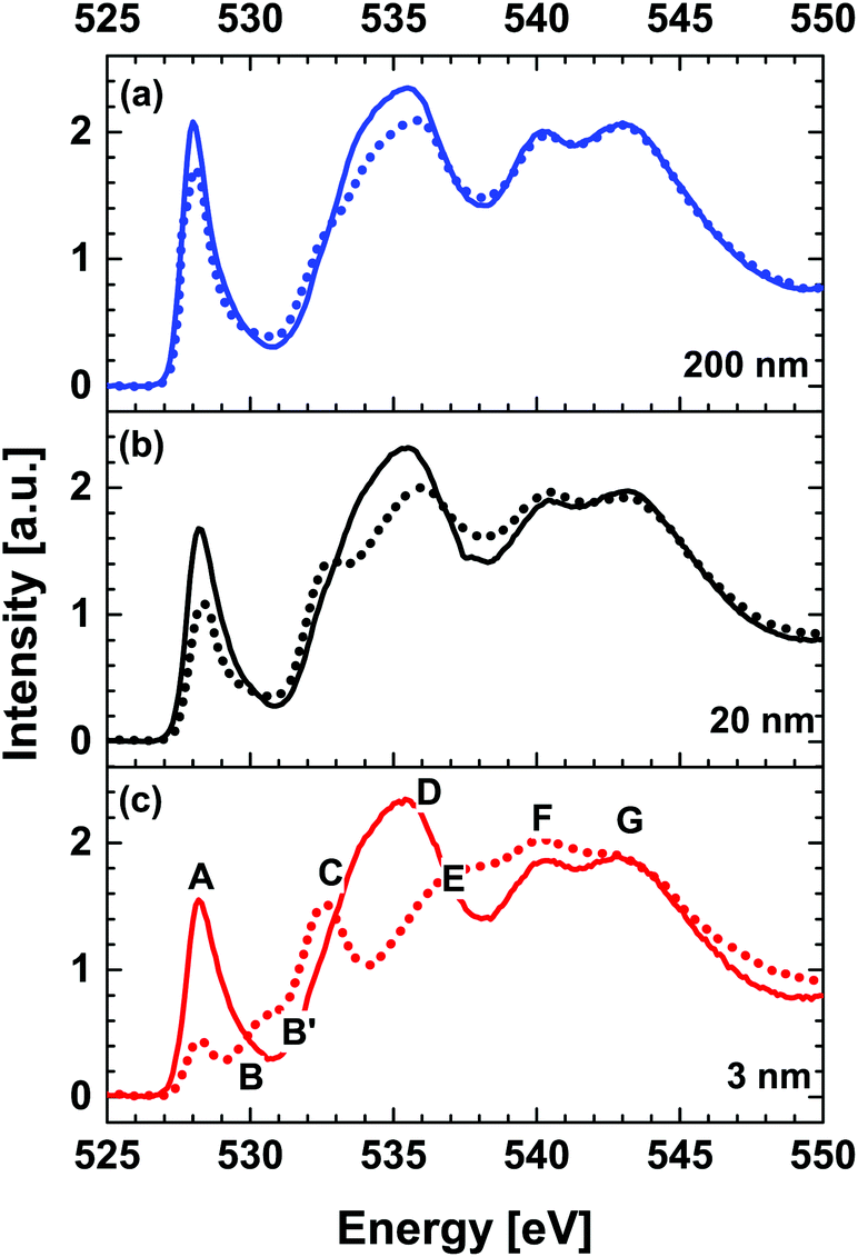 | ||
| Fig. 3 Thickness dependent comparison of O K-edge XANES spectra acquired at room temperature (RT) (solid line) and 78 K (dotted line) for (a) 200 nm, (b) 20 nm and (c) 3 nm NNO films. | ||
Negligible differences in the intensities of the shape-resonance are recorded for all NNO thicknesses. More significant reduction of peak A and enhancement of peak B are observed for the 3 nm NNO film across the MIT. For this sample, a noticeable increase in the intensity of the shape-resonance, which can be directly associated with Ni2+ states (refer to peak B′ of the red dotted spectrum in Fig. 3(c)), is observed and it is related to the reduced dimensionality effects as reported in ref. 19. In this study, the competition between the strain and dimensionality effects on MIT evolution in NNO films is reported. The NNO thickness of 20 u.c. (∼8 nm) was determined as the critical thickness below which the dimensionality effects are dominant and above which strain effects determine phase evolution. Both effects are crystallographic structure phenomena, but one is lattice distortion that leads to an increase of the Ni 3d bandwidth and hence favors metallic phase, and the other is reduction in dimensions that largely affects electron correlation. Reduced dimensionality of ultrathin NNO films (3 nm) results in a decrease of the O 2p–Ni 3d covalent bandwidth (see Table 1, integrated intensity values for A_B) and hence the insulating phase is favored. In addition, the disorder effects associated with reduced dimensionality can lead to localisation of electrons, explaining its insulating nature.9,36 As reported in the work by Scherwitzl et al.,24 utilisation of the electric double layer transistor method may resolve issues related with the presence of different strain states. We are considering extending the current study and reporting results in a separate paper.
| Int. intensity | A–B | C | D | E–F | ||||
|---|---|---|---|---|---|---|---|---|
| RT | 78 K | RT | 78 K | RT | 78 K | RT | 78 K | |
| 200 nm | 3.35 | 2.98 | 1.88 | 1.84 | 4.52 | 3.95 | 8.78 | 8.74 |
| 20 nm | 2.94 | 2.07 | 1.91 | 2.00 | 4.42 | 3.60 | 8.52 | 8.98 |
| 3 nm | 2.88 | 1.52 | 1.92 | 2.08 | 4.49 | 2.50 | 8.49 | 9.27 |
Ni L32 edge
Fig. 4 shows Ni L32-edge XANES spectra for 200 nm NNO/STO samples along with powder reference compounds, representing Ni ions having formal valence of Ni2+ (NiO, grey line), Ni3+ (LiNiO2, green line) and calculated spectrum of Ni3+ (circle scatters), adopted from ref. 37 at RT. Following the dipole selection rule, the Ni L32-edge XANES spectra illustrate a transition from Ni 2p → 3d states. Typically, the integrated intensity can be directly related to the total number of empty 3d states at Ni sites. As can be seen in Fig. 4, an experimental XANES spectrum of 200 nm NNO/STO films displays much broader features compared to NiO and LiNiO2 powder reference spectra. For the NiO powder reference, spectral features are consistent with previously-reported data and theoretical calculations.38–41 As compared to the calculated Ni3+ spectrum, the lack of the spectral weight in the energy region denoted A/B (∼855 eV) for the Ni3+ powder reference can be understood as a result of in-vacuum sputtering performed prior to spectra acquisition. For 200 nm NNO/STO film spectra, the lack of an overall fine structure, especially the absence of peak (a), see the calculated Ni3+ spectrum, can be regarded as an accumulative effect of (i) spectral resolution available at the SINS beamline as well as (ii) the crystal and ligand field splitting value (10Dq) used in the calculations.42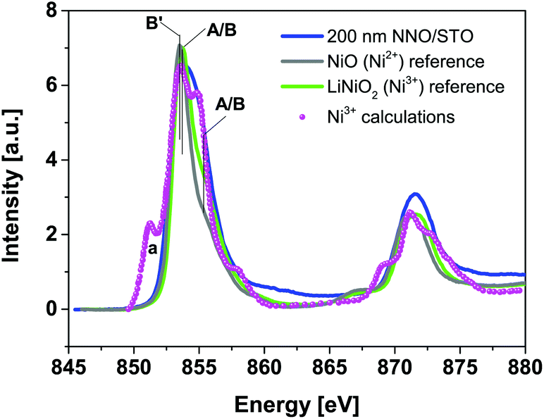 | ||
| Fig. 4 Room-temperature Ni L32-edge XANES spectra of 200 nm NNO/STO (blue solid line) and NiO (grey line), and LiNiO2 (green line) powder reference compounds and the calculated spectrum of Ni3+ (magenta circle scatters), adopted from ref. 37. | ||
Fingerprint analysis of Ni L32-edge XANES spectra with references does not exclude a possibility of multiple valency (mixed-valence) of nickel ions in the NNO films. Recorded data suggest that the majority of nickel ions in the NNO films are in a Ni3+ state (refer to peaks labelled A/B (855 eV)), with a slight contribution from a Ni2+ state. This argument is also supported by Ni K-edge and XPS data (RT only) (refer to ESI Fig 4 and 6(a)†). In general, determination of the oxidation state of elements is associated with sensitive and straightforward techniques, such as X-ray photoemission spectroscopy (XPS). However, at 78 K, all the investigated samples are insulating. Therefore, the application of the XPS technique is challenged by the charging effect. The charging effect influences the energies of detected electrons and hence causes shifts of XPS features.22 In contrast, the XANES technique is not affected by charging effects. The energy is defined by the incident radiation and so the effect of charging will not cause shifts of spectral features.43,44 In the attempt, to avoid sample modification to enable XPS measurements for the insulating phase, the XANES technique was adequately applied to specify the valence state of Ni (and Nd).
Fig. 5 shows a thickness dependent comparison of Ni L32-edge XANES spectra acquired at RT (solid line) and 78 K (dashed line). Comparison of spectra acquired at RT reveals that the majority of nickel ions in the NNO films are in a Ni3+ state with a varying contribution from a Ni2+ state.
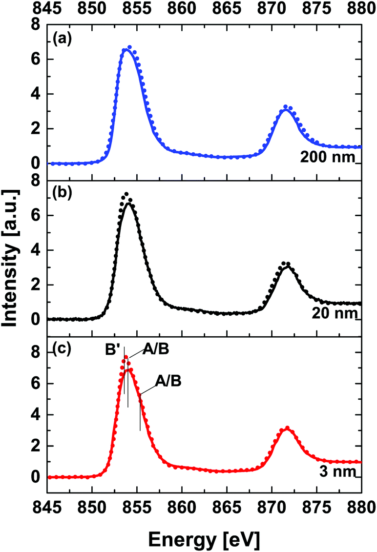 | ||
| Fig. 5 Thickness dependent comparison of Ni L32-edge XANES spectra at room temperature (solid line) and 78 K (dotted line) for (a) 200 nm, (b) 20 nm and (c) 3 nm NNO films. | ||
The ratio of Ni2+/Ni3+ decreases with increasing the thickness of the NNO film. In general, the area ratio between the L3 and L2 peaks can provide an estimation of the Ni valence state. Higher valence of the cation gives rise to a smaller ratio of L3/L2.45 The data shown in Table 2 support the above statement. For thin film samples, spectra acquired at 78 K are somewhat different (higher intensity) from RT spectra at the energy position of peak B′ (at about 853.7 eV, e.g. related to Ni2+-like states). This observation can be related to electron localization at Ni2+-like states (refer to ESI Fig. 5†). We argue that this can be viewed as direct evidence of (partial) charge disproportion at Ni sites accompanied by a structural symmetry change. For the 200 nm NNO film, viewed as a reference for the bulk, the intensity of the peak A/B (at about 854.3 eV, e.g. related to Ni(3±δ)+ states) is somewhat higher at 78 K.
| Int. intensity ratio (L3/L2) | RT | LT |
|---|---|---|
| 200 nm | 1.70 (∼Ni3+) | 1.68 (∼Ni(3+δ)+) |
| 20 nm | 1.75 | 1.71 |
| 3 nm | 1.76 (∼Ni3+/Ni2+) | 1.72 (∼Ni3+/Ni(3−δ)+) |
The ratio of integrated intensities L3/L2 is somewhat lower at 78 K for all samples, see Table 2. This observation suggests that instead of the commonly-accepted idea of charge localization at Ni2+ sites being solely responsible for the stabilization of the insulating phase below the MIT, our data suggest a scenario where disproportioned insulating states can be related to alternating Ni(3±δ)+ states.
Nd M54 edge
Fig. 6 shows Nd M54-edge XANES spectra for a 200 nm NNO/STO sample (solid blue line) along with powder reference compounds (Nd2O3, solid cyan line), representing Nd ions having a formal valence of Nd3+ recorded at RT.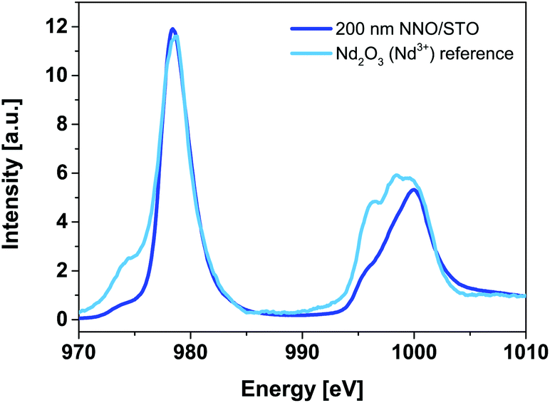 | ||
| Fig. 6 Room-temperature Nd M54-edge XANES spectra of 200 nm NNO/STO (blue solid line) and Nd2O3 (cyan solid line) powder reference compounds. Our reference compound data are consistent with experimental data of bulk NNO reported elsewhere29,30 and suggest that the valency of Nd ions matches well with that of Nd3+. | ||
The Nd M54-edge probes the unoccupied density of the Nd 4f states and illustrates multiplet splitting caused mainly by the hole in the Nd 3d level and the partly-filled 4f state. It is generally accepted that the main criteria used in XANES fingerprint analysis are: (i) shape, (ii) energy position and (iii) intensity of the main shape-resonances. Among these, the energy position of shape-resonances is most sensitive to changes in the valence state of the parent metal. In Fig. 6, no shift is observed, as the energy position of the main shape resonance (978.4 eV) of the 200 nm NNO/STO spectra is identical to the Nd2O3 powder reference compound. Therefore we conclude that the valency of Nd ions matches well with that of Nd3+. Our data are consistent with experimental data of bulk NNO reported elsewhere.29,30
Fig. 7 shows a thickness dependent comparison of Nd M54-edge XANES spectra acquired at RT (solid line) and 78 K (dashed line). The main shape resonances M5- and M4-edge are observed at 978.4 eV and at 1000.2 eV, respectively. This indicates that Nd ions remain in a 3+ state for all three samples. The sensitivity/resolution of the XANES technique does not allow us to neglect the fact that the FWHM is narrower for the spectra obtained at 78 K.
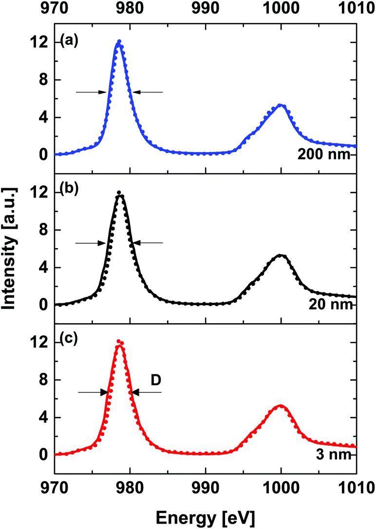 | ||
| Fig. 7 Thickness dependent comparison of Nd M54-edge XANES spectra at room temperature (solid line) and 78 K (dotted line) for (a) 200 nm, (b) 20 nm and (c) 3 nm NNO films. | ||
Without noticeable differences in energy position, this can be attributed to a narrowing of the overlap between Nd–Nd and as a consequence of changes in the Nd–(O–Ni) interaction, e.g. weakening of rare earth metal–transition metal hybridization strength (covalency). Narrowing of the d-band in complex compounds was predicted using the d-band center model developed by Hammer and Nørskov.46,47 A temperature dependent weakening of intermetallic interaction is also observed in the O K-edge XANES (see Fig. 3), where at low temperature the decrease of peak intensity (D) compared to RT data can be assigned to increased electron density at the hybridized metal–oxygen orbitals involving Nd 5sp and O 2p.
Traditionally, most efforts to describe the properties of RNiO3 compounds are attributed to Ni 3d–O 2p hybridization changes. Here we adapt a scheme where the interactions between rare earth and transition metals are also of great essence. The strength of intermetallic interaction, e.g. between Ni 3d and Nd 4f, is influenced by the degree of Ni 3d–O 2p covalency (hybridization strength). A schematic illustration representing the complex interconnection and co-dependency of covalency in RNiO3 is shown in Fig. 8. The arrows represent the hypothetical and equivalent hybridization strengths of Ni 3d–O 2p (left), Nd 4f–O 2p (right) and intermetallic Ni 3d–Nd 4f charge transfer (CT).
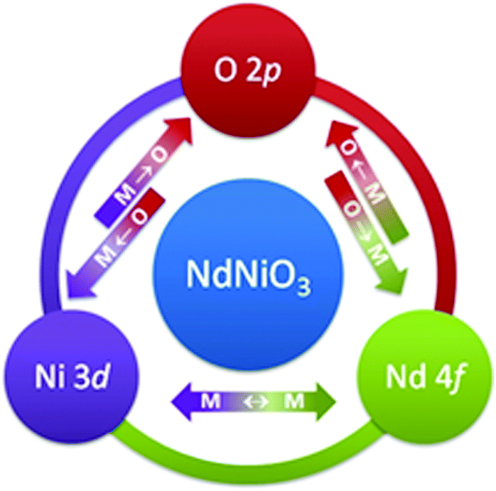 | ||
| Fig. 8 Schematic illustration representing the complex interconnection and co-dependency of covalency in RNiO3 compounds. | ||
Discussion
In this work, NNO thin films are studied as representative examples to investigate the ground state electronic structure of nickelates. Interpretation of the MIT phenomenon in NNO mainly centers on where the band gap comes from. Torrance et al. argued that the band gaps open between the Ni 3d states and the O 2p orbitals.48 However, Park et al. proposed that the Coulomb force of repulsion between electrons causes the electrons to localize and then the band gap opens between the occupied and unoccupied Ni 3d bands.49 In addition, Johnston et al. used exact diagonalization and Hartree–Fock calculations and confirmed that a strong electron–lattice coupling provides distortions and drives the system through a MIT.50 Recently, Bisogni et al. presented evidence that these materials exhibit a negative charge-transfer energy and a MIT can be interpreted in terms of bond disproportionation leading to two Ni site configurations. These sites differ in the hybridization with the O 2p hole states, e.g. the opening of a O–O gap while the charge at the Ni sites is almost equal.51Here, we focus on the detailed description of site-selective XANES spectral changes observed at RT and 78 K to resolve aspects of electronic structure modification and correlate it with a hypothesis of driving forces behind the MIT mentioned above. Based on the knowledge gathered so far, it is known that a purely ionic description of the ground state for NiO6 octahedra 3d72p6 cannot accurately illustrate the electronic configuration of the R3+Ni3+(O2−)3 perovskite compounds. Various experimental and theoretical studies support hypotheses that include hybridization (covalency) of the ground state |ΨGhyb〉 = α|3d72p6〉 + β|3d8〉 + γ|3d92〉. Here, α2 + β2 + γ2 = 1 values can be found by different spectroscopic techniques. O K-edge XANES is only sensitive to intra-atomic transition matrix elements. Therefore, the integrated intensity of shape-resonances A and B (528 eV, Fig. 2) is proportional to β2 and is a measure of the covalency in the ground state. By analogy, in a NiO reference compound, the integrated intensity of the shape resonance labelled B′ (532 eV) is a measure of covalency in the ground state, dominated by the contribution from |3d9〉. From Fig. 2, the integrated intensity of peaks A and B (refer to 200 nm NNO) is higher compared to the integrated intensity of peak B′ (refer to reference NiO), indicating that at RT the Ni 3d–O 2p hybridization in NNO is stronger than that in NiO. This observation hints at the importance of the interaction between rare earth and transition metals in nickel perovskites, supporting the idea of complex interaction as shown in Fig. 8. Additionally, data shown in Table 1 point towards the decrease of Ni 3d–O 2p covalency with the decreasing thickness of NNO films, which is even more pronounced at 78 K, referring to integrated intensity values (A_B). The decrease in the Ni 3d–O 2p hybridization (less efficient overlap between Ni 3d and O 2p orbitals) can be understood as charge localization between two Ni site configurations, namely Ni 3d8 and Ni 3d82 (refer to the observed concurrent decrease of the intensity of peak A_B and the increase of peak C in Fig. 3). Charge fluctuation of this type is only possible in the presence of O 2p–O 2p hole interactions strong enough to split the O 2p band (p–p gap). This seems to be the case for the insulating phase of NNO. The gap opening explains the increase in Rsheet with the decreasing thickness of NNO films observed across the whole temperature range in Fig. 1.
From the data accumulated at the Ni L32-edge it is evident that the idea of partial charge disproportionality between Ni sites can be adopted to describe the temperature and thickness driven changes in the electronic configuration of the NNO/STO system. Recent work describing charge disproportionality phenomena suggests that due to the proximity of partly occupied O 2p and initially empty Ni 3d levels, some O 2p electrons can be transferred to Ni 3d levels (leaving a hole in the O 2p band). For the NNO system (Ni3+) this should be traced to an increased Ni2+/Ni3+ ratio, which is observed in the temperature dependent XANES data in Fig. 5 and the data in the ESI (Fig. 5†). Therefore, we conclude that at temperatures below TMI, charge disproportionality at Ni sites which is accompanied by a decrease of Ni 3d–O 2p covalency results in gap opening (due to the splitting of the O 2p band) and is the main factor that stabilizes the insulating phase in NNO films.
Following the schematic illustration in Fig. 8, a temperature dependent decrease of Ni 3d–O 2p covalency should also influence the strength of the Nd 4f–O 2p hybridization. This suggestion is consistent with a dramatic decrease of the intensity of peak D in O K-edge XANES spectra at RT and 78 K (Fig. 3). Additionally, a narrowing of the FWHM of the Nd M5-edges main peak at 78 K as compared to RT data (Fig. 7) is observed, supporting the complex interconnection and co-dependency of covalency in RNiO3 in Fig. 8. At low temperature, Ni 3d orbitals become more localized between Ni(3±δ)+ sites. The scenario where bond disproportionation stabilizes the insulating phase is preferred as compared to a hypothesis of charge localization at Ni2+ sites. As shown in ESI Fig. 3,† a substantial spectral weight which can be associated solely with Ni2+ sites (see the area shaded in light green and labelled as B′) is only detected for the 3 nm NNO film (refer to the dotted line in ESI Fig. 3(c)).†. As mentioned above, it is should be associated with a dominant influence of dimensionality effects. Dimensionality effects at NNO thicknesses above 20 u.c. are negated by stress phenomena. Therefore, for 20 nm and 200 nm NNO samples no contribution to spectral weight which can be associated solely with Ni2+ sites is detected (ESI Fig. 3†). On the contrary, most temperature dependent alterations of spectral weight are detected in the energy range assigned to oxygen 2p states hybridized with Nd (5d, 4f) states (refer to the second derivative data shown in ESI Fig. 3,† the area shadowed in light purple and labelled C, D). Following the schematic illustration in Fig. 8 this is a consequence of decreased Ni 3d–O 2p covalency, explained earlier as localization between two Ni site configurations, namely Ni 3d8 and Ni 3d82 (disproportionation). In addition, the Nd M5-edge FWHM is narrower for the spectra obtained at 78 K than at RT. This can be attributed to a narrowing of the overlap between Nd–Nd and therefore a weakening of rare earth metal–transition metal hybridization strength (covalency).
Conclusions
We demonstrate that a thorough investigation of XANES spectra can be used as a reference method to probe changes in the electronic structure of complex oxide heterostructures. Analysis of XANES spectra suggests that: (i) nominally trivalent Ni ions exhibit charge disproportionality in NNO films, (ii) the decrease of the Ni 3d–O 2p hybridization driven by the presence of strong O 2p–O 2p hole interaction at low temperature enables the opening of the p–p gap, and (iii) intermetallic hybridization should not be overlooked and should be treated in terms of overall metal d-band narrowing. For a NNO film exhibiting a sharp MIT, Ni 3d electron localization, e.g. the concurrent existence of Ni 3d8 and Ni 3d82 states, is responsible for the observed transition. At temperatures below the MIT the O 2p–O 2p hole correlation is strong enough to split the O 2p band stabilizing insulating phase. Electronic localization does not conflict with widely-discussed structural changes above and below the transition temperature.
Acknowledgements
This work was supported by the Singapore National Research Foundation under its Competitive Research Funding (NRF-CRP 82011-06 and NRF2008NRF-CRP002024), MOE-AcRF-Tier-2 (MOE2015-T2-1-099), NUS-YIA, and FRC. J. Wang thanks the Ministry of Education, Singapore for financial support under project no. MOE2013-T2-1-052 and MOE2014-T2-1-099. We would like to extend our appreciation to Mr Lim Chee Wai and Mr Wong How Kwong for technical support.Notes and references
- J. B. Torrance, P. Lacorre, A. I. Nazzal, E. J. Ansaldo and C. Niedermayer, J. Solid State Chem., 1991, 91, 225 CrossRef.
- J. L. García-Muñoz, J. Rodriguez-Carvajal, P. Lacorre and J. B. Torrance, Phys. Rev. B: Condens. Matter Mater. Phys., 1992, 46, 4414 CrossRef.
- J. S. Zhou, J. B. Goodenough and B. Dabrowski, Phys. Rev. Lett., 2005, 94, 226602 CrossRef PubMed.
- M. Zaghrioui, A. Bulou, P. Lacorre and P. Laffez, Phys. Rev. B: Condens. Matter Mater. Phys., 2001, 64, 081102(R) CrossRef.
- J. L. García-Muñoz, M. A. G. Aranda, J. A. Alonso and M. J. Martinez-Lope, Phys. Rev. B: Condens. Matter Mater. Phys., 2009, 79, 134432 CrossRef.
- S. Lee, R. Chen and L. Balents, Phys. Rev. Lett., 2011, 106, 016405 CrossRef PubMed.
- H. Y. Hwang, Y. Iwasa, M. Kawasaki, B. Keimer, N. Nagaosa and Y. Tokura, Nat. Mater., 2012, 11, 103 CrossRef CAS PubMed.
- B. Lau and A. J. Millis, Phys. Rev. Lett., 2013, 110, 126404 CrossRef PubMed.
- M. L. Medarde, J. Phys.: Condens. Matter, 1997, 9, 1679 CrossRef CAS.
- I. V. Nikulin, M. A. Novojilov, A. R. Kaul, S. N. Mudretsova and S. V. Kondrashov, Mater. Res. Bull., 2004, 39, 775 CrossRef CAS.
- A. Tiwari and K. P. Rajeev, Solid State Commun., 1998, 109, 119 CrossRef.
- H. Yamada, Y. Ogawa, Y. Ishii, H. Sato, M. Kawasaki, H. Akoh and Y. Tokura, Science, 2004, 305, 646 CrossRef CAS PubMed.
- J. Reiner, F. Walker and C. Ahn, Science, 2009, 323, 1018 CrossRef CAS PubMed.
- G. Catalan, Phase Transitions, 2008, 81, 729 CrossRef CAS.
- A. Tiwari, C. Jin and J. Narayan, Appl. Phys. Lett., 2002, 80, 4039 CrossRef CAS.
- D. A. Dikin, M. Mehta, C. W. Bark, C. M. Folkman, C. B. Eom and V. Chandrasekhar, Phys. Rev. Lett., 2011, 107, 056802 CrossRef CAS PubMed.
- K. A. Gschneidner, J. Less-Common Met., 1971, 25, 405 CrossRef CAS.
- N. Palina, A. Annadi, T. C. Asmara, C. Diao, X. Yu, M. B. Breese and A. Rusydi, Phys. Chem. Chem. Phys., 2016, 18, 13844 RSC.
- L. Wang, S. Ju, L. You, Y. Qi, Y. W. Guo, P. Ren, Y. Zhou and J. Wang, Sci. Rep., 2015, 5, 18707 CrossRef CAS PubMed.
- L. Wang, S. Dash, L. Chang, L. You, Y. Feng, X. He and S. Wang, ACS Appl. Mater. Interfaces, 2016, 8, 9769 CAS.
- X. Yu, O. Wilhelmi, H. O. Moser, S. V. Vidyaraj, X. Gao, A. T. S. Wee, T. Nyunt, H. Qian and H. Zheng, J. Electron Spectrosc. Relat. Phenom., 2005, 144–147, 1031 CrossRef CAS.
- J. Cazaux, J. Electron Spectrosc. Relat. Phenom., 1999, 105, 155 CrossRef CAS.
- G. Ertl and J. Kueppers, Low Energy Electrons and Surface Chemistry, VCH, 1985 Search PubMed.
- R. Scherwitzl, P. Zubko, I. G. Lezama, S. Ono, A. F. Morpurgo, G. Catalan and J. M. Triscone, Adv. Mater., 2010, 22(48), 5517 CrossRef CAS PubMed.
- P. Kuiper, G. Kruizinga, J. Ghijsen, G. A. Sawatzky and H. Verweij, Phys. Rev. Lett., 1989, 62(2), 221 CrossRef CAS PubMed.
- R. J. Mossanek, G. Domínguez-Cañizares, A. Gutiérrez, M. Abbate, D. Díaz-Fernández and L. Soriano, J. Phys.: Condens. Matter, 2013, 25(49), 495506 CrossRef CAS PubMed.
- M. Abbate, G. Zampieri, F. Prado, A. Caneiro, J. M. Gonzalez-Calbet and M. Vallet-Regi, Phys. Rev. B: Condens. Matter Mater. Phys., 2002, 65(15), 155101 CrossRef.
- V. Scagnoli, U. Staub, M. Janousch, G. I. Meijer, L. Paolasini, F. D'Acapito, J. G. Bednorz and R. Allenspach, J. Magn. Magn. Mater., 2004, 272, 420 CrossRef.
- M. A. Hayward and M. J. Rosseinsky, Solid State Sci., 2003, 5, 839 CrossRef CAS.
- M. Medarde, A. Fontaine, J. L. Garcia-Munoz, J. Rodriguez-Carvajal, M. De Santis, M. Sacchi, G. Rossi and P. Lacorre, Phys. Rev. B: Condens. Matter Mater. Phys., 1992, 46, 14975 CrossRef CAS.
- M. Alexander, H. Romberg, N. Nücker, P. Adelmann, J. Fink, J. T. Markert, M. B. Maple, S. Uchida, H. Takagi, Y. Tokura and A. C. W. P. James, Phys. Rev. B: Condens. Matter Mater. Phys., 1991, 43(1), 333 CrossRef CAS.
- A. Bashir, M. Ikram, R. Kumar, P. Thakur, K. H. Chae, W. K. Choi and V. R. Reddy, J. Phys.: Condens. Matter, 2009, 21(32), 325501 CrossRef PubMed.
- W. L. Jang, Y. M. Lu, C. L. Dong, W. S. Hwang, P. H. Hsieh, C. L. Chen and T. S. Chan, Sci. Adv. Mater., 2013, 5(10), 1346 CrossRef CAS.
- M. Finazzi and N. B. Brookes, Phys. Rev. B: Condens. Matter Mater. Phys., 1999, 60(8), 5354 CrossRef CAS.
- M. L. Medarde, J. Phys.: Condens. Matter, 1997, 9(8), 1679 CrossRef CAS.
- J. Billy, V. Josse, Z. Zuo, A. Bernard, B. Hambrecht, P. Lugan, D. Clément, L. Sanchez-Palencia, P. Bouyer and A. Aspect, Nature, 2008, 453(7197), 891 CrossRef CAS PubMed.
- I. Preda, M. Abbate, A. Gutierrez, S. Palacín, A. Vollmer and L. Soriano, J. Electron Spectrosc. Relat. Phenom., 2007, 156, 111 CrossRef.
- L. Soriano, A. Gutiérrez, I. Preda, S. Palacín, J. M. Sanz, M. Abbate, J. F. Trigo, A. Vollmer and P. R. Bressler, Phys. Rev. B: Condens. Matter Mater. Phys., 2006, 74, 193402 CrossRef.
- G. Van der Laan, J. Zaanen, G. A. Sawatzky, R. Karnatak and J.-M. Esteva, Phys. Rev. B: Condens. Matter Mater. Phys., 1986, 33(6), 4253 CrossRef CAS.
- R. J. Green, M. W. Haverkort and G. A. Sawatzky, Phys. Rev. B: Condens. Matter Mater. Phys., 2016, 94(19), 195127 CrossRef.
- C. Piamonteze, F. M. F. De Groot, H. C. N. Tolentino, A. Y. Ramos, N. E. Massa, J. A. Alonso and M. J. Martínez-Lope, Phys. Rev. B: Condens. Matter Mater. Phys., 2005, 71(2), 020406 CrossRef.
- J. Van Elp, B. G. Searle, G. A. Sawatzky and M. Sacchi, Solid State Commun., 1991, 80(1), 67 CrossRef CAS.
- B. Gilbert, R. Andres, P. Perfetti, G. Margaritondo, G. Rempfer and G. de Stasio, Ultramicroscopy, 2000, 83, 129–139 CrossRef CAS PubMed.
- B. K. Agarwal, X-ray Spectroscopy-An Introduction, Springer-Verlag, 1991 Search PubMed.
- L. Wang, L. Chang, X. Yin, L. You, J. L. Zhao, H. Guo, K. Jin, K. Ibrahim, J. Wang, A. Rusydi and J. Wang, Appl. Phys. Lett., 2017, 110(4), 043504 CrossRef.
- B. Hammer and J. K. Nørskov, Surf. Sci., 1995, 343(3), 211 CrossRef CAS.
- B. Hammer and J. K. Nørskov, Adv. Catal., 2000, 45, 71 CAS.
- J. B. Torrance, P. Lacorre, A. I. Nazzal, E. J. Ansaldo and C. Niedermayer, Phys. Rev. B: Condens. Matter Mater. Phys., 1992, 45(14), 8209 CrossRef CAS.
- H. Park, A. J. Millis and C. A. Marianetti, Phys. Rev. Lett., 2012, 109(15), 156402 CrossRef PubMed.
- S. Johnston, A. Mukherjee, I. Elfimov, M. Berciu and G. A. Sawatzky, Phys. Rev. Lett., 2014, 112(10), 106404 CrossRef PubMed.
- V. Bisogni, S. Catalano, R. J. Green, M. Gibert, R. Scherwitzl, Y. Huang, V. N. Strocov, P. Zubko, S. Balandeh, J. M. Triscone and G. Sawatzky, Nat. Commun., 2016, 7, 13017 CrossRef CAS PubMed.
Footnote |
| † Electronic supplementary information (ESI) available: NNO_ESI_NP.pdf. See DOI: 10.1039/c7nr00742f |
| This journal is © The Royal Society of Chemistry 2017 |