
 Open Access Article
 This Open Access Article is licensed under a Creative Commons Attribution-Non Commercial 3.0 Unported Licence
Band-edge oscillator strength of colloidal CdSe/CdS dot-in-rods: comparison of absorption and time-resolved fluorescence spectroscopy†
I.
Angeloni
ab,
W.
Raja‡
ac,
A.
Polovitsyn
ac,
F.
De Donato
a,
R. Proietti
Zaccaria
*a and
I.
Moreels
 *a
*a
aIstituto Italiano di Tecnologia, via Morego 30, 16163 Genova, Italy. E-mail: iwan.moreels@iit.it; remo.proietti@iit.it
bDipartimento di Chimica e Chimica Industriale, Università di Genova, Via Dodecaneso 33, 16146 Genova, Italy
cDipartimento di Fisica, Università di Genova, Via Dodecaneso 33, 16146 Genova, Italy
First published on 6th March 2017
Abstract
We studied the oscillator strength fgap of the band gap transition in heteronanocrystals (hNCs) with a spherical CdSe core embedded in an elongated CdS shell. A comparison with fgap of core-only CdSe NCs confirmed a reduction of the electron–hole overlap in hNCs with a band gap larger than 2.05 eV or smaller than 1.98 eV. However, the decrease in fgap is limited to about 50% when compared to CdSe NCs, suggesting that residual confinement still localizes the electron near the core. We correlated fgap with the radiative lifetime obtained from multiexponential photoluminescence (PL) decay traces. The different components were attributed to radiative decay, or deep and shallow carrier trapping, respectively, using the PL quantum efficiency (QE) as a guideline. Our data highlight the challenges associated when extracting the radiative decay, and demonstrate the added value of absorption spectroscopy to obtain the band-edge oscillator strength and the associated radiative recombination rate in colloidal hNCs.
Introduction
Narrow emission linewidths over a wide spectral range, together with the possibility to fine-tune their optical properties via size, shape and composition are key qualities that make semiconductor nanocrystals (NCs) frontier materials for optoelectronic applications, along with the versatility and low-cost nature of the colloidal synthesis routes employed to produce them. In the last few years several procedures have been developed to encapsulate the core into a shell made of a second semiconductor.1–4 The obtained hetero-structure NCs (hNCs) multiply the possibilities to control the optical properties, via the engineering of the conduction band (CB) and valence band (VB) alignment of core and shell. It is thus possible to obtain structures in which electrons and holes are both confined to the same region, as in the case of type I CdSe/ZnS1 core/shell NCs, or in which electrons and holes are confined to different materials, as in type II ZnSe/CdS,2,5 CdTe/CdSe,3 or CdSe/ZnTe4 NCs. CdSe/CdS NCs form a particular case. Because of the small offset in the CB of the two materials, the hole is localized in the core while the electron delocalizes into the CdS shell and remains bound to the hole via Coulomb interactions. For this reason, CdSe/CdS hNCs are usually referred to as quasi-type-II structures, and they are among the most studied hNCs to date.The actual degree of delocalization still varies between different reports. Optical measurements and theoretical calculations6,7 have suggested that the electron can strongly delocalize along the CdS rod length, while scanning tunneling spectroscopy (STS) experiments have supported a type-I band offset with electrons and holes both confined to the CdSe core.8 More recent work suggested that the core diameter plays a distinctive role in the electron delocalization, as CdSe/CdS hNCs showed a transition from a type-I to a quasi-type-II regime when the core becomes sufficiently small.9–11 Processing hNCs into thin films may also affect the optical properties, as CdSe/CdS dot-in-rod (DiR) aerogels showed an increase of the electron delocalization due to DiR coupling.12
Measurements of the photoluminescence (PL) lifetime have often been used to support the quasi-type-II behavior of CdSe/CdS hNCs. Although in principle straightforward, the correlation of the electron–hole overlap with lifetime depends on several factors. Most importantly, the influence of nonradiative recombination that competes with the radiative relaxation channel must be taken into account, often accomplished via determination of the NC PL quantum efficiency (QE).
In this work we studied the band edge optical properties of wurtzite CdSe NCs and CdSe/CdS DiRs using optical absorption spectroscopy which, through the absorption cross section, allows us to access the band-edge oscillator strength, an intrinsic material property. Finite element simulations were performed to obtain the electric field profile inside the CdSe core, considering the non-analytical shape of the hNC – i.e., a spherical core located at one side of a rod-shaped shell – and the presence of an organic ligand shell. The resulting band edge oscillator strength fgap reveals a reduced electron–hole overlap only for DiRs with either a small (diameter smaller than about 3.5 nm) or a large (diameter larger than about 4.5 nm) CdSe core. The data are then compared to time-resolved PL spectroscopy, which allows us to reassess the role of the PL QE in determining the radiative recombination dynamics. As for the absorption measurements, both DiRs with a core diameter below 3.5 nm and above 4.5 nm show a reduced electron–hole overlap.
Experimental
Materials
Trioctylphosphine oxide (TOPO, 99%), trioctylphosphine (TOP, 97%), cadmium oxide (CdO, 99.999%), sulfur powder (99%), and selenium powder (99.99%) were purchased from Strem Chemicals. Cadmium oxide (CdO, 99.5%) was purchased from Sigma-Aldrich. Octadecylphosphonic acid (ODPA, 99%) and hexylphosphonic acid (HPA, 99%) were purchased from Polycarbon Industries.Synthesis
To synthesize CdSe cores (QD1 to QD5 shown in Table S2†), TOPO (3 g), ODPA (0.280 mg), and CdO (0.060 g, Strem Chemicals) were mixed in a 25 mL three-necked flask and heated to ca. 120 °C for 1 hour.7 Then, under a nitrogen atmosphere, the solution was heated to 380 °C to completely dissolve the CdO. When the solution became colorless, 1.5 mL of TOP was injected and the temperature was allowed to recover to 380 °C. Se:TOP (0.058 g Se dissolved in 0.500 g TOP) was injected at 380 °C and the growth time was varied to obtain different sizes of CdSe NCs. After synthesis, the NCs were purified three times by precipitation and re-dispersion, using toluene as a solvent and methanol as a non-solvent. The sample was finally dispersed in 3 mL of toluene.A second set of CdSe cores (QD6 to QD14 in Table S2†) was synthesized by mixing TOPO (3.0 g), ODPA (0.280 g) and CdO (0.060 g, Sigma-Aldrich) in a 50 mL flask. The mixture was heated to ca. 150 °C under vacuum for about 1 hour. Then, under a nitrogen atmosphere, the solution was heated to above 300 °C to dissolve the CdO until it turned optically clear. Next, 1.5 g of TOP was injected into the flask and the temperature was allowed to recover to 370 °C for the injection of the Se:TOP solution (0.058 g Se with 0.360 g TOP). The reaction time was modified in order to synthesize CdSe NCs of different sizes. After the synthesis, the NCs were purified as described above. Both types of CdSe cores were used as seeds in the synthesis of CdSe/CdS DiRs, according to the procedure of Carbone et al.7
Characterization
Transmission electron microscopy (TEM) images were collected by drop casting a dilute suspension of NCs on a carbon coated 200 mesh copper grid and imaging them with a JEOL JEM 1011 TEM equipped with a thermo-ionic source (tungsten filament) operating at 100 kV. The diameter of the CdSe cores was calculated using the calibration curve proposed by Jasieniak et al.,13 while the dimensions of the CdSe/CdS DiRs were estimated from TEM images using about 100–200 NCs.UV-Vis absorption spectra were obtained with a Varian Cary 300 UV-vis spectrophotometer. Photoluminescence measurements were performed with an Edinburgh Instruments FLS920 spectrofluorometer. Samples were dispersed in chloroform and excited by using a xenon lamp coupled with a monochromator set at 530 nm (10 nm bandwidth). PL decay traces were collected in time-correlated single photon mode. Samples were excited with a 50 ps, 405 nm pulsed laser, and the PL decay was measured in a region of typically 10 nm around the emission maximum. A pulse period of 2 μs was chosen to ensure full decay between the pulses. The traces were fitted using a sum of three exponential functions. For each sample, we analysed the three time constants resulting from the fit to relate them to radiative processes, hole trapping in mid-gap states14 or delayed emission.15 Finally an area-weighted average lifetime τavg was calculated including only the components which were considered to constitute the radiative decay.
The PL QE was measured using an integrating sphere. Samples were excited at 530 nm with a xenon lamp, and the optical density at the excitation wavelength was adjusted to 0.1 or lower. The accuracy of the system was verified using a solution of Rhodamine 101 in ethanol.16 The obtained QE value of 94% ± 7% is in close agreement with literature values.17 To analyse the relation between QE and radiative lifetime, for three representative samples additional PL QE measurements were performed with an excitation wavelength of 405 nm (the typical wavelength used for PL decay measurements), and in addition the PL decay was collected with a 510 nm pulsed laser (close to that of the 530 nm used in the QE measurements).
Finite element simulations
In the case of non-analytical shapes such as our CdSe/CdS DiRs that are composed of a CdSe core located near one end of an elongated CdS shell, numerical models are required to evaluate the dielectric screening.18 We performed 3D finite element numerical simulations (COMSOL multiphysics) to examine the near field optical properties of hNCs and calculate the electric field inside the CdSe core. The simulation domain comprised a spherical volume representing a CdSe/CdS DiR embedded in chloroform. The refractive index of chloroform was taken from Samoc.19 We used a plane wave as external excitation, hence allowing for the employment of the scattered field formulation, where only the scattered solution needs to be computed. The wavelength λ = 610 nm has been chosen as a typical value for the first excitonic transition of our dataset. Perfectly matched layer (PML) boundary conditions were used to avoid undesired reflections. Based on the polarisation of the incident external electric field (Eext = 1 V m−1), either parallel or perpendicular to the major axis of the nanorod which coincides with the CdSe/CdS c-axis in wurtzite NCs,7,20 appropriate dielectric constants for CdSe (εreal,|| = 6.980, εreal,⊥ = 6.904) and CdS (εreal,|| = 6.627, εreal,⊥ = 6.625) were selected. Values were taken from bulk data at the respective band edges (1.75 eV for CdSe,21 2.42 eV for CdS22), with the imaginary part of both set to zero, as we can assume εimag ≪ εreal near the band edge,23 and applying a reduction of 15% due to residual quantum confinement effects.18,24 We previously found that the dielectric function in CdSe/CdS hNCs is somewhat reduced compared to bulk at 4.2 eV.18 Since bulk εreal is nearly flat in the energy range between 4.2 eV and the band edge,24 we applied the same 15% reduction to the CdS and CdSe optical constants at the band edge. In our simulations, we considered a CdSe core diameter of 4 nm, with a total diameter of 5.5 nm, representative for the experimental samples used. We also added a 1.8 nm shell with a refractive index of 1.6 to account for the organic ligands.18 The DiR aspect ratio (AR) was varied between 1 and 25. In addition, we have also evaluated the influence of the position of the CdSe core on the electric field profile, by moving it from 10% (i.e., near the DiR tip) to 50% (at the center of the DiR) of the total rod length. The resulting electric field profile was averaged over the CdSe core volume, from which the local field factor fLF in the parallel and perpendicular directions was calculated as the ratio of this average value to the applied Eext.Results and discussion
At energies well above the band gap, the absorption spectrum of colloidal NCs is no longer significantly affected by quantum confinement,13,25–28 and the discrete optical transitions typical of a confined system pass into a bulk-like density of states. As a consequence, the absorption spectra of NCs of different sizes converge, and it has been shown for several materials27 that an intrinsic absorption coefficient μi can be defined, which depends only on the NC volume fraction f in suspension: | (1) |
In the case of CdSe/CdS DiRs, we showed in our previous work18 that μi also depends on the overall NC AR and on the volume ratio of the CdSe core and CdS shell. We proposed a general function to calculate μi of CdSe/CdS hNCs at 4.2 eV that incorporates the effects of AR and the volume ratio. Here we make use of this function to calculate the intrinsic absorption spectra for all NCs as μ(v) = (μ4.2/A4.2)·A(v). Representative μi-spectra of CdSe/CdS DiRs are shown in Fig. 1a.
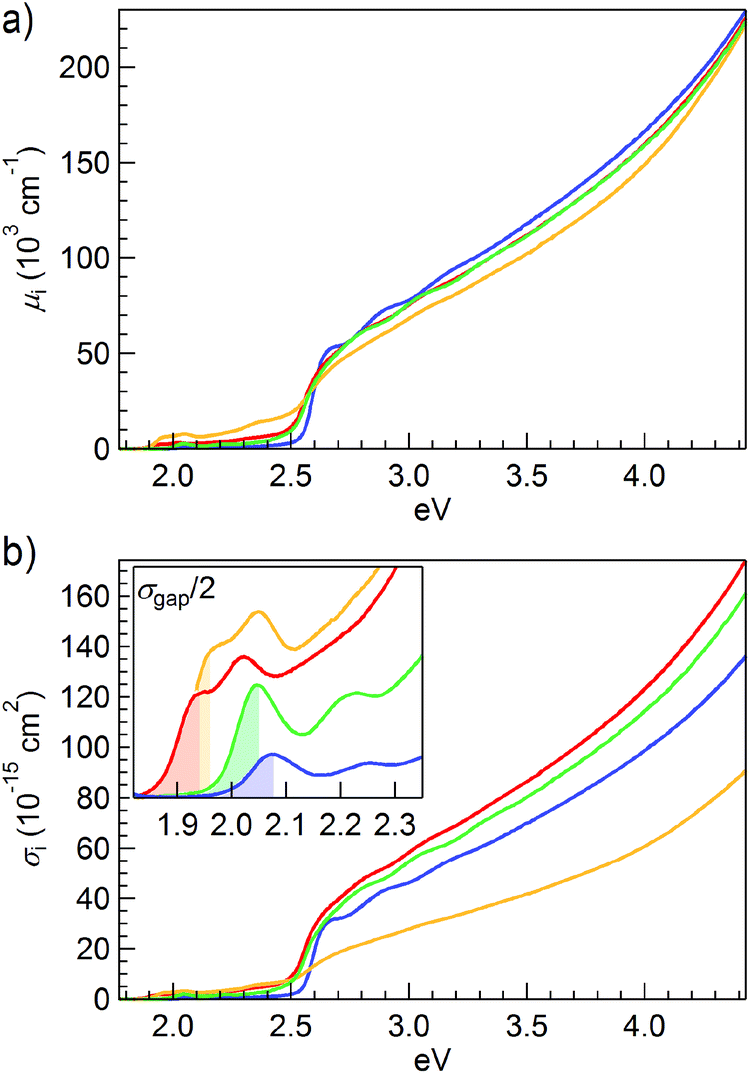 | ||
| Fig. 1 μ i (a) and σi (b) spectra of representative DiRs (NR7, NR10, NR20 and NR23 of Table S1,† plotted in blue, green, yellow and red lines, respectively). The inset in panel b shows a zoom of the core region. We highlighted the area under the low-energy half of the first absorption peak. | ||
As μi depends on the core-to-shell volume ratio, band-edge absorption properties are more conveniently analyzed using the absorption cross section σi = VNC·μi, since it expresses the properties of a single NC (VNC equals the NC volume). The σi-spectra are shown in Fig. 1b. The energy-integrated absorption cross section σgap of the band edge transition is obtained by doubling the integral of the low energy half of the first absorption peak in the σi-spectra, as depicted in the inset of Fig. 1b, according to procedures applied previously to PbSe,27 PbS27 and PbSe/CdSe NCs.29 If some scattering was present in the band edge region, we subtracted a linear background from the σi-spectrum before the integration.
The oscillator strength fgap is related to σgapvia the local field factor fLF, which expresses the ratio between the electric field inside the particle and the external applied electric field:27
 | (2) |
First, we calculated σgap and fgap for CdSe cores. We approximated them as spheres, which allows for an analytical calculation of fLF![[thin space (1/6-em)]](https://www.rsc.org/images/entities/char_2009.gif) 27,30 (see ESI, section 2.1†). With fgap ranging from 2.4 to 8.1 for 2.3 nm to 6.1 nm NCs, the values follow the same trend as reported by Čapek et al.23 for zinc blende CdSe NCs (see ESI, section 3† for detailed calculations). The somewhat lower fgap obtained here stems mainly from the reduced CdSe optical constants used.
27,30 (see ESI, section 2.1†). With fgap ranging from 2.4 to 8.1 for 2.3 nm to 6.1 nm NCs, the values follow the same trend as reported by Čapek et al.23 for zinc blende CdSe NCs (see ESI, section 3† for detailed calculations). The somewhat lower fgap obtained here stems mainly from the reduced CdSe optical constants used.
While the dielectric screening and thus fLF of a concentric spheroid can be expressed in a closed form,31,32 a numerical finite-element simulation is needed when non-analytical shapes are involved.18,33–35 Since the band-edge absorption in our hNCs mainly takes place near the CdSe core, we calculated fLF from the electric field Eloc inside the core. The NCs were modeled as cylinders capped by two hemispheres. Because of the symmetry of the structure, the polarization which builds up in response to an applied external field is parallel to it, and so is the resulting field inside the NC.18 Hence, it is sufficient to compute Eloc in the two cases where the external field is parallel and perpendicular to the major axis of the rod, and obtain the average field intensity as |Eloc|2 = (|E|||2 + 2|E⊥|2)/3. With an applied external field Eext = 1 V m−1 in the finite-element simulation, the averaged |Eloc|2 coincides with |fLF|2.
Different approaches have been reported in literature to estimate the position of the CdSe core in CdSe/CdS DiRs synthesized by seeded growth. Quantitative analysis on high-resolution TEM (HR-TEM) images performed by Carbone et al.7 situated the core at about 1/3–1/4 of the total rod length. This estimate was later confirmed by selective growth of gold onto the CdSe region of CdSe/CdS DiRs.36 A more symmetric position of the core along the rod (about 45% of the total length) has been estimated recently by Diroll et al.37 on the basis of annular dark field scanning TEM measurements, revealing that the actual core position may depend somewhat on the synthesis conditions. The core position also varies with the overall rod length, being closer to the NC center for short rods, and gradually shifting toward one tip for longer samples.38,39 In order to evaluate the influence of the core position on the electric field profile, we performed a finite element simulation in which the seed was moved from a position at 10% to 50% of the total rod length. The results show a 15% increase of |fLF|2 as the CdSe core is located closer to the rod center (see ESI, section 2.2†). Note that the changes in |fLF|2 are more pronounced near the tips, where we find the strongest non-uniformity of the electric field. |fLF|2 only changes by 3% when the position is varied from 30% to the center of the DiR.
Considering the above results, we located the core at 30% of the total length for further calculations. The simulated electric field magnitude along the rod is shown in Fig. 2a for a NC with AR = 7.5. As expected, the increasing AR leads to a larger |fLF|2 (Fig. 2b). Simulated data have been fitted using exponential functions y = y0 + Aexp(−Bx) (|fLF,|||2: y0 = 0.971, A = −0.882, B = 0.346; |fLF,⊥|2: y0 = 0.242, A = 0.227, B = 0.711) to obtain |fLF|2 for each DiR sample and, through eqn (2), fgap. The details of the calculation of fgap are reported in the ESI, section 4.†
 | ||
| Fig. 2 (a) Magnitude |Eloc| of the electric field which builds up inside the DiR in response to an external applied electric field Eext of 1 V m−1 at 610 nm, when Eext is parallel (left) or perpendicular (right) to the NC major axis (AR = 7.5). Consistent with literature, the CdSe core was located at 30% of the total NC length. (b) Values of |fLF|2 simulated for DiRs with ARs from 1 to 25 (markers) and fit to the data (dashed lines). Parallel and perpendicular components of |fLF|2 are plotted with blue circles and diamonds, respectively. The green triangles and line report |fLF|avg2, the weighted average of the data and fit. | ||
f gap eliminates the role of fLF and the associated shape-dependent σgap, and hence is more suitable to compare spherical core and rod-like core/shell NCs with respect to the electron–hole overlap. We plotted fgapversus the band gap E0 for DiRs (full circles) and CdSe NCs (open circles, see ESI, Tables S1 and S2† for E0 values) shown in Fig. 3, which allows comparison of core and core/shell NCs that exhibit similar quantum confinement.40 Indeed, as was demonstrated for CdSe and PbX (X = S, Se) quantum dots (QDs),27fgap increases for larger sizes, which prohibits comparison on the basis of a similar core diameter. Additionally, fgap is frequency-dependent, further motivating the use of E0 as a reference.41 In DiRs with a core diameter below ca. 3.5 nm (E0 > 2.05 eV, see color bar in Fig. 3) a reduction of fgap of about 50% can be appreciated. In an intermediate diameter regime (3.5 nm < d < 4.5 nm or 1.98 eV < E0 < 2.05 eV, see color bar in Fig. 3), fgap for DiRs is in line with the ones of CdSe cores. For particles with a core larger than 4.5 nm, the values fall again below the ones of CdSe NCs with the same absorption gap. Note that in DiRs with a large core, however, the first absorption peak is not clearly resolved, as is the case for smaller cores (see inset in Fig. 1, yellow and red curves), which could yield a slightly larger uncertainty for fgap.
 | ||
| Fig. 3 Oscillator strength fgap, calculated for CdSe/CdS DiRs (full symbols) and CdSe cores (empty symbols). The dashed line is a fit (y = 1.6 + 5711x−10) to fgap of CdSe NCs. The color code for DiRs indicates the diameter of the CdSe core. All values have been plotted with respect to the NC band gap E0. | ||
In samples with small cores strong quantum confinement, in combination with a reduced conduction band offset, allows the electron to delocalize into the shell, yielding the expected reduction in fgap due to a quasi-type-II band alignment. The significant red shift of the band edge after shell growth supports this model (ESI, Fig. S3†). Large core samples however show a reduced fgap despite a much smaller band edge red shift, suggesting that a different mechanism is responsible for the electron–hole separation. The results are in line however with the calculations of Segarra et al.,42 who showed that strain at the CdSe/CdS interface can lead to a reduced electron–hole overlap, which in this case can occur in the absence of a significant reduction of the NC band gap. Fig. 3 also shows considerable variation in the oscillator strength of CdSe/CdS DiRs, even for samples with the same absorption gap and a similar core diameter (e.g. light blue points). In order to unveil a possible dependence on the DiR geometry (AR, NC diameter or shell thickness), we considered a subset of data with core sizes between 3.3 and 3.5 nm. Surprisingly, no clear trends were found (see ESI, section 6†). This indicates that the oscillator strength is determined not only by the core and shell geometry, the synthesis details and associated CdSe/CdS interface properties – e.g. strain43 or interface barriers44 – will lead to a further modification of fgap. Indeed, literature studies showing delocalization effects are usually performed on samples synthesized using the same seed, or even prepared taking aliquots from the same synthesis, to improve consistency within the sample set.9
We therefore restricted our analysis to three subsets (distinguished by colors shown in Fig. 4a–c), each of them consisting of samples synthesized using the same core (cores up to 3.5 nm). For each of the three subsets, we have grown an increasingly thicker CdS shell. The larger CdSe/CdS diameter measured by TEM is confirmed by the corresponding red shift of the CdS absorption gap around 500 nm, as was also observed by Adel et al.45 (Fig. 4a, see also ESI, section 7† for details of the calculation). One sample showed an unexpectedly small CdS band gap (indicated with an arrow) and is reported in the subsequent panels but not considered further in the analysis of fgap. The increasing diameter also leads to a reduced band gap (Fig. 4b) and for each of the core diameters we observed a concomitant reduction of fgap (Fig. 4c). Both trends confirm that the electron delocalizes into the CdS shell, and suggest that the delocalization and thus the electron–hole overlap are mainly determined by the overall diameter of the DiR, as was also observed by Rainò et al.46 using time-resolved PL spectroscopy.
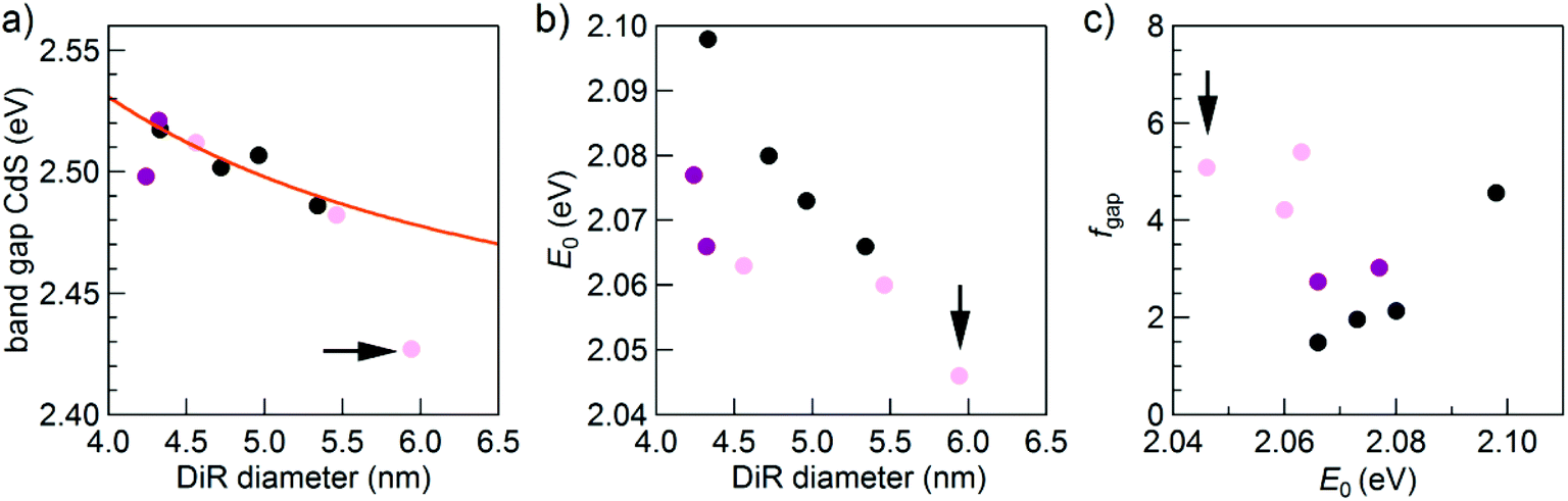 | ||
| Fig. 4 Analysis of three subsets of core/shell DiRs synthesized from the same cores (purple: core diameter of 3.3 nm, black: 3.4 nm, and pink: 3.5 nm). (a) The red shift of the shell absorption onset is in agreement with the larger hNC diameter measured by TEM, except for the sample indicated by the arrow. (b) For each of the three subsets, a larger shell diameter corresponds to a smaller band gap. (c) A smaller band gap also leads to a reduced fgap. | ||
The absorption oscillator strength fgap, or more directly the absorption cross section σgap of the band-edge transition can be related to the spontaneous emission rate τrad−1via Fermi's golden rule:47
 | (3) |
 | ||
| Fig. 5 (a) Scheme of the carrier relaxation pathways, highlighting the relaxation processes that lead to radiative emission (full arrows) and the non-radiative recombination (dashed arrows). k denotes the rates at which each process occurs. (b) PL decay traces of a representative DiR (NR12 in Table S1†) upon excitation at 405 nm (green trace) and 510 nm (orange trace). QE values at 405 nm and 530 nm are also reported. | ||
To verify the influence of the QE on the radiative lifetime, we measured the PL decay of 3 representative samples, exciting them at both 405 nm – which is the typical excitation wavelength used throughout our measurements – and 510 nm, a wavelength below the CdS band gap that directly excites CdSe core states. The resulting curves were fitted with a multi-exponential function using three decay constants. In Fig. 5b, while the QE changes by almost a factor of 2 between 405 nm and 530 nm, the decay traces exciting at 405 and 510 nm diverge only in the long tail. Assigning the first two components to the radiative recombination (cf. analysis below and in the ESI, section 9†), the lifetimes calculated are almost identical, yielding 22.8 ns and 20.4 ns when exciting at 405 nm and 510 nm, respectively (Table 1). Other samples show a similar behavior (see ESI, section 8†). It confirms that the QE of CdSe/CdS DiRs, excited at 405 nm, is mainly determined by nonradiative recombination of charge carriers in the CdS shell,38 and the recombination dynamics of core excitons is largely independent of the excitation wavelength (and thus of the PL QE). The PL QE is not unity even when exciting the DiRs at 530 nm, yet this may be due to the existence of a dark fraction of NCs.50 Hence, in the subsequent analysis we do not rely on the QE as a conversion factor between the measured and the radiative lifetime and use it only to classify the DiRs and understand the PL decay dynamics.
| λ ex | τ 1 (w1) | τ 2 (w2) | τ rad | τ 3 (w3) |
|---|---|---|---|---|
| 405 nm | 15.8 ns (46%) | 29.6 ns (48%) | 22.8 ns | 203.4 ns (6%) |
| 510 nm | 10.8 ns (15%) | 22.2 ns (79%) | 20.4 ns | 79.9 ns (6%) |
We measured the PL QE (λex = 530 nm, i.e., excitation below the CdS absorption edge), and collected the decay traces of several DiR samples (λex = 405 nm), which were then again fitted with a multi-exponential function with three components. By analyzing the lifetime and their relative weights, we attributed these individual components to either radiative decay, fast hole trapping, or shallow electron trapping that induces a long-lifetime tail. A detailed discussion of the analysis is reported in the ESI, section 9.† Briefly, when the PL QE falls below 60%, some DiRs show a low-weight PL component with a lifetime below 10 ns, which we considered to be due to nonradiative trapping. On the other hand, independent of the PL QE almost all samples revealed a long-lifetime component with a lifetime above 100 ns, which was assigned to delayed emission.15 The remaining component(s) were used to calculate τrad. A plot of the lifetime components against PL QE, with open symbols marking trapping and closed symbols marking radiative processes, is shown in Fig. 6a. Note that, with respect to the dataset used for the oscillator strength calculation (see above), one sample has been discarded because of a PL QE below 3% (NR22 in Table S1†).
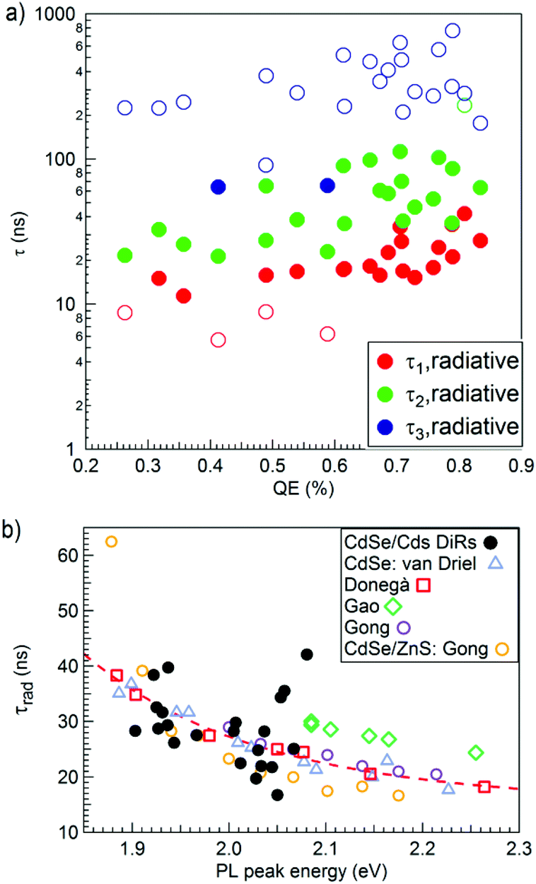 | ||
| Fig. 6 (a) Lifetime components obtained from the multi-exponential fit of the DiRs, plotted with respect to the PL QE. Closed (open) symbols represent components which have been attributed to radiative (trapping) processes. (b) Comparison of τrad calculated for our DiRs with literature data on CdSe NCs. | ||
τ rad is compared with literature data for CdSe cores14,51–53 shown in Fig. 6b (see ESI, section 10† for details). As for the analysis of fgap, the CdSe cores compare well with DiRs between 1.98 and 2.05 eV, in agreement with a negligible electron delocalization. Note that, depending on the AR, the lifetimes of DiRs can even be faster (up to 38%) than CdSe QDs with a similar band gap, due to a larger average local field factor for anisotropic particles (Fig. 2, green triangles). On the other hand, for small and large cores, with a band gap above 2.05 eV or below 1.98 eV, respectively, τrad exceeds the CdSe core-only QDs. However, with overall values below 50 ns, τrad is almost one order of magnitude smaller than in spherical CdSe/CdS giant shell NCs, where τrad can extend to 500 ns.20,54 This highlights the importance of the NC size and shape in determining the electron–hole overlap in CdSe/CdS quasi-type-II hNCs via quantum confinement, more specifically strong 2D electron confinement along the radial direction in DiRs vs. residual weak 3D confinement in giant-shell dot-in-dots (DiDs), and the shape-dependent electron–hole Coulomb interactions and dielectric screening.20,54
Using eqn (3), we obtained the emission oscillator strength fgap,PL from τrad, which we compared with fgap calculated from the absorption cross section (denoted as fgap,abs in Fig. 7a). While reasonable agreement between the two is obtained for samples with a small core using g = 8, a clear deviation is observed for other samples. By assuming that the total oscillator strength of the transitions involved in the band-edge absorption and emission should be equal, we can derive an effective degeneracy g of the transition. As shown in Fig. 7b, g can reach values ranging from 4 up to 21 for DiRs (full symbols). The deviation from g = 8 is not specific to CdSe/CdS DiRs, as we also calculated a continuous increase with core diameter for CdSe QDs (solid line). Likely, it is due to the energy separation between the bands, which in both cases is strongly reduced for larger QDs, resulting in a larger manifold of states located under the first absorption peak. This was also reported by Gong et al.,40 who demonstrated that a thermal population of the 1p3/2 hole level has to be taken into account at room temperature, as the energy distance between the 1se–1s3/2 and 1se–1p3/2 states is in the range of 21 to 57 meV for particles from 5.5 to 2.5 nm. These values are comparable with the typical FWHM of the first absorption peak of our samples (see ESI, Table S1†). A similar conclusion was drawn for CdTe NCs by Kamal et al.,55 where good agreement between experimental and measured data was found only when assuming g = 16.
 | ||
| Fig. 7 (a) Comparison of the oscillator strength values fgap,abs obtained from the absorption cross section with fgap,PL calculated from the radiative lifetimes, assuming a band gap degeneracy of 8. (b) Effective degeneracy of the band edge transition calculated from the ratio between fgap,abs and fgap,PL for DiRs (full symbols, with the colour representing fgap,abs). Similar results for CdSe NCs (solid black line, derived from the fitted curves to the CdSe data shown in Fig. 3 and 6b). | ||
Conclusions
We combined absorption and PL spectroscopy to study the band-edge optical properties of CdSe/CdS hNCs. To this end, fgap is a most convenient quantity, as it directly correlates with the electron–hole overlap and hence gives insight into the degree of electron delocalization into the CdS shell. We obtained fgap for CdSe cores through a calibration of the NC absorbance spectra at high energy and analytical calculation of the electric field inside the core, while finite element simulations were needed for the DiRs, as the rod-like shape of the shell leads to a non-uniform internal electric field. The comparison of fgap for CdSe NCs and CdSe/CdS DiR hNCs shows a reduced electron–hole overlap both in the limit of small (below 3.5 nm) and large (above 4.5 nm) CdSe core diameters. While in the first case this is the result of electron delocalization into the CdS shell, with the extent of delocalization mainly determined by the rod diameter, in the latter it is possibly enabled by strain at the core/shell interface.42 Independent results are obtained when fgap,PL is calculated from the radiative lifetimes via Fermi's golden rule. Here, contributions to the decay traces were separated into radiative processes and nonradiative trapping, and we observed that the PL QE cannot be used to directly extract τrad from the measured PL decay time. fgap,PL obtained from the DiR radiative decay corroborated the results from absorption spectroscopy. Different from spherical giant-shell CdSe/CdS DiDs, where radiative lifetimes can reach 500 ns,20,54 radiative lifetimes remain overall shorter than 50 ns in DiRs, making them ideal candidates for applications where a high absorption cross section and PL QE need to be combined with fast recombination rates.56,57Acknowledgements
The present publication is realized with the support of the Ministero degli Affari Esteri e della Cooperazione Internazionale (IONX-NC4SOL).References
- M. A. Hines and P. Guyot-Sionnest, J. Phys. Chem., 1996, 100, 468–471 CrossRef CAS.
- A. Nemchinov, M. Kirsanova, N. N. Hewa-Kasakarage and M. Zamkov, J. Phys. Chem. C, 2008, 112, 9301–9307 CAS.
- D. Oron, M. Kazes and U. Banin, Phys. Rev. B: Condens. Matter, 2007, 75, 035330 CrossRef.
- S. Kim, B. Fisher, H.-J. Eisler and M. Bawendi, J. Am. Chem. Soc., 2003, 125, 11466–11467 CrossRef CAS PubMed.
- D. Dorfs, A. Salant, I. Popov and U. Banin, Small, 2008, 4, 1319–1323 CrossRef CAS PubMed.
- J. Müller, J. M. Lupton, P. G. Lagoudakis, F. Schindler, R. Koeppe, A. L. Rogach, J. Feldmann, D. V. Talapin and H. Weller, Nano Lett., 2005, 5, 2044–2049 CrossRef PubMed.
- L. Carbone, C. Nobile, M. De Giorgi, F. D. Sala, G. Morello, P. Pompa, M. Hytch, E. Snoeck, A. Fiore, I. R. Franchini, M. Nadasan, A. F. Silvestre, L. Chiodo, S. Kudera, R. Cingolani, R. Krahne and L. Manna, Nano Lett., 2007, 7, 2942–2950 CrossRef CAS PubMed.
- D. Steiner, D. Dorfs, U. Banin, F. Della Sala, L. Manna and O. Millo, Nano Lett., 2008, 8, 2954–2958 CrossRef CAS PubMed.
- A. Sitt, F. D. Sala, G. Menagen and U. Banin, Nano Lett., 2009, 9, 3470–3476 CrossRef CAS PubMed.
- H. Eshet, M. Grünwald and E. Rabani, Nano Lett., 2013, 13, 5880–5885 CrossRef CAS PubMed.
- X. Wen, A. Sitt, P. Yu, Y.-R. Toh and J. Tang, Phys. Chem. Chem. Phys., 2012, 14, 3505–3512 RSC.
- S. Sánchez-Paradinas, D. Dorfs, S. Friebe, A. Freytag, A. Wolf and N. C. Bigall, Adv. Mater., 2015, 27, 6152–6156 CrossRef PubMed.
- J. Jasieniak, L. Smith, J. van Embden, P. Mulvaney and M. Califano, J. Phys. Chem. C, 2009, 113, 19468–19474 CAS.
- Y. Gao and X. Peng, J. Am. Chem. Soc., 2015, 137, 4230–4235 CrossRef CAS PubMed.
- F. T. Rabouw, M. Kamp, R. J. A. van Dijk-Moes, D. R. Gamelin, A. F. Koenderink, A. Meijerink and D. Vanmaekelbergh, Nano Lett., 2015, 15, 7718–7725 CrossRef CAS PubMed.
- M. J. Barthel, I. Angeloni, A. Petrelli, T. Avellini, A. Scarpellini, G. Bertoni, A. Armirotti, I. Moreels and T. Pellegrino, ACS Nano, 2015, 9, 11886–11897 CrossRef CAS PubMed.
- M. Grabolle, M. Spieles, V. Lesnyak, N. Gaponik, A. Eychmüller and U. Resch-Genger, Anal. Chem., 2009, 81, 6285–6294 CrossRef CAS.
- I. Angeloni, W. Raja, R. Brescia, A. Polovitsyn, F. De Donato, M. Canepa, G. Bertoni, R. Proietti Zaccaria and I. Moreels, ACS Photonics, 2016, 3, 58–67 CrossRef CAS.
- A. Samoc, J. Appl. Phys., 2003, 94, 6167–6174 CrossRef CAS.
- S. Christodoulou, G. Vaccaro, V. Pinchetti, F. De Donato, J. Q. Grim, A. Casu, A. Genovese, G. Vicidomini, A. Diaspro, S. Brovelli, L. Manna and I. Moreels, J. Mater. Chem. C, 2014, 2, 3439 RSC.
- S. Ninomiya and S. Adachi, J. Appl. Phys., 1995, 78, 4681–4689 CrossRef CAS.
- S. Ninomiya and S. Adachi, J. Appl. Phys., 1995, 78, 1183–1190 CrossRef.
- R. K. Čapek, I. Moreels, K. Lambert, D. De Muynck, Q. Zhao, A. Van Tomme, F. Vanhaecke and Z. Hens, J. Phys. Chem. C, 2010, 114, 6371–6376 Search PubMed.
- M. Alves-Santos, R. D. Felice and G. Goldoni, J. Phys. Chem. C, 2010, 114, 3776–3780 CAS.
- C. A. Leatherdale, W.-K. Woo, F. V. Mikulec and M. G. Bawendi, J. Phys. Chem. B, 2002, 106, 7619–7622 CrossRef CAS.
- P. Yu, M. C. Beard, R. J. Ellingson, S. Ferrere, C. Curtis, J. Drexler, F. Luiszer and A. J. Nozik, J. Phys. Chem. B, 2005, 109, 7084–7087 CrossRef CAS PubMed.
- Z. Hens and I. Moreels, J. Mater. Chem., 2012, 22, 10406 RSC.
- M.-A. Langevin, D. Lachance-Quirion, A. M. Ritcey and C. N. Allen, J. Phys. Chem. C, 2013, 117, 5424–5428 CAS.
- B. De Geyter, Y. Justo, I. Moreels, K. Lambert, P. F. Smet, D. Van Thourhout, A. J. Houtepen, D. Grodzinska, C. de Mello Donega, A. Meijerink, D. Vanmaekelbergh and Z. Hens, ACS Nano, 2011, 5, 58–66 CrossRef CAS PubMed.
- C. F. Bohren and D. R. Huffman, Absorption and Scattering of Light by Small Particles, Wiley-VCH Verlag GmbH, 1998 Search PubMed.
- A. H. Sihvola and J. A. Kong, IEEE Trans. Geosci. Remote Sens., 1988, 26, 420–429 CrossRef.
- S. Giordano, J. Electrost., 2003, 58, 59–76 CrossRef.
- J. Venermo and A. Sihvola, J. Electrost., 2005, 63, 101–117 CrossRef.
- A. Sihvola, P. Yla-Oijala, S. Jarvenpaa and J. Avelin, IEEE Trans. Antennas Propag., 2004, 52, 2226–2233 CrossRef.
- A. Mejdoubi and C. Brosseau, Phys. Rev. E: Stat. Phys., Plasmas, Fluids, Relat. Interdiscip. Top., 2006, 74, 031405 CrossRef PubMed.
- G. Menagen, D. Mocatta, A. Salant, I. Popov, D. Dorfs and U. Banin, Chem. Mater., 2008, 20, 6900–6902 CrossRef CAS.
- B. T. Diroll, N. Gogotsi and C. B. Murray, Chem. Mater., 2016, 3345–3351 CrossRef CAS.
- K. Wu, L. J. Hill, J. Chen, J. R. McBride, N. G. Pavlopolous, N. E. Richey, J. Pyun and T. Lian, ACS Nano, 2015, 9, 4591–4599 CrossRef CAS PubMed.
- E. Yoskovitz, G. Menagen, A. Sitt, E. Lachman and U. Banin, Nano Lett., 2010, 10, 3068–3072 CrossRef CAS PubMed.
- K. Gong, Y. Zeng and D. F. Kelley, J. Phys. Chem. C, 2013, 117, 20268–20279 CAS.
- J. Johansen, S. Stobbe, I. S. Nikolaev, T. Lund-Hansen, P. T. Kristensen, J. M. Hvam, W. L. Vos and P. Lodahl, Phys. Rev. B: Condens. Matter, 2008, 77, 073303 CrossRef.
- C. Segarra, J. I. Climente, A. Polovitsyn, F. Rajadell, I. Moreels and J. Planelles, J. Phys. Chem. Lett., 2016, 7, 2182–2188 CrossRef CAS PubMed.
- F. Rajadell, M. Royo and J. Planelles, J. Appl. Phys., 2012, 111, 014303 CrossRef.
- N. J. Borys, M. J. Walter, J. Huang, D. V. Talapin and J. M. Lupton, Science, 2010, 330, 1371–1374 CrossRef CAS PubMed.
- P. Adel, J. Bloh, D. Hinrichs, T. Kodanek and D. Dorfs, Z. Phys. Chem., 2016, 93–106 Search PubMed.
- G. Rainò, T. Stöferle, I. Moreels, R. Gomes, Z. Hens and R. F. Mahrt, ACS Nano, 2012, 6, 1979–1987 CrossRef PubMed.
- E. Merzbacher, Quantum Mechanics, Wiley International Edition, New York, 2nd edn, 1970 Search PubMed.
- D. V. Talapin, J. H. Nelson, E. V. Shevchenko, S. Aloni, B. Sadtler and A. P. Alivisatos, Nano Lett., 2007, 7, 2951–2959 CrossRef CAS PubMed.
- C. She, A. Demortière, E. V. Shevchenko and M. Pelton, J. Phys. Chem. Lett., 2011, 2, 1469–1475 CrossRef CAS.
- N. Durisic, A. G. Godin, D. Walters, P. Grütter, P. W. Wiseman and C. D. Heyes, ACS Nano, 2011, 5, 9062–9073 CrossRef CAS PubMed.
- A. F. van Driel, G. Allan, C. Delerue, P. Lodahl, W. L. Vos and D. Vanmaekelbergh, Phys. Rev. Lett., 2005, 95, 236804 CrossRef CAS PubMed.
- C. de Mello Donegá and R. Koole, J. Phys. Chem. C, 2009, 113, 6511–6520 Search PubMed.
- H.-M. Gong, Z.-K. Zhou, H. Song, Z.-H. Hao, J.-B. Han, Y.-Y. Zhai, S. Xiao and Q.-Q. Wang, J. Fluoresc., 2007, 17, 715–720 CrossRef CAS PubMed.
- S. Brovelli, R. D. Schaller, S. A. Crooker, F. García-Santamaría, Y. Chen, R. Viswanatha, J. A. Hollingsworth, H. Htoon and V. I. Klimov, Nat. Commun., 2011, 2, 280 CrossRef CAS PubMed.
- J. S. Kamal, A. Omari, K. Van Hoecke, Q. Zhao, A. Vantomme, F. Vanhaecke, R. K. Capek and Z. Hens, J. Phys. Chem. C, 2012, 116, 5049–5054 CAS.
- A. Castelli, F. Meinardi, M. Pasini, F. Galeotti, V. Pinchetti, M. Lorenzon, L. Manna, I. Moreels, U. Giovanella and S. Brovelli, Nano Lett., 2015, 15, 5455–5464 CrossRef CAS PubMed.
- E. Jang, S. Jun, H. Jang, J. Lim, B. Kim and Y. Kim, Adv. Mater., 2010, 22, 3076–3080 CrossRef CAS PubMed.
Footnotes |
| † Electronic supplementary information (ESI) available: Details of the material properties, finite element simulations, calculations of the oscillator strength, comparison of the oscillator strength with literature, dependence of the oscillator strength on DiR geometry, details on the estimation of the CdS band gap, and lifetime analysis. See DOI: 10.1039/c6nr09021d |
| ‡ Current address: Nanooptische Konzepte für die PV, Helmholtz-Zentrum Berlin, H.-Meitner-Platz 1, 14109, Germany. |
| This journal is © The Royal Society of Chemistry 2017 |