
Precise regulation of tilt angle of Si nanostructures via metal-assisted chemical etching†
Fei
Teng
,
Ning
Li
,
Daren
Xu
,
Dongyang
Xiao
,
Xiangchao
Yang
and
Nan
Lu
*
State Key Laboratory of Supramolecular Structure and Materials, College of Chemistry, Jilin University, Changchun 130012, PR China. E-mail: luenan@jlu.edu.cn; Fax: +86-431-85168477; Tel: +86-431-85168477
First published on 29th November 2016
Abstract
The ability to regulate the tilt angle of Si nanostructures is important for their applications in photoelectric devices. Herein we demonstrate a facile method to precisely regulate the tilt angle of nanocones with metal-assisted chemical etching (MaCE) in a one-step process based on the systematic investigation of the formation mechanism of the tilt angle. With Au nanohole arrays as templates, the tilt angles of Si nanocone arrays can be tuned from 69.2° to 88.6° by varying the composition of the etchant. When the Si nanocone arrays are the same height (2.2 μm), the reflectivity decreases with the decreasing of the tilt angle. When the tilt angle is 83.0°, the average reflectivity is lowered to 1.37% in the 250–1000 nm range. This method can be applied for fabrication over a large area (as large as 2 cm × 2 cm). This chemical method should be applicable to other Si nanostructures, which may promote the applications of MaCE in semiconductor manufacturing.
Introduction
Si nanostructures have been widely applied in the fields of nanoelectronics, opto-electronics, and energy conversion and storage, as well as in biosensors and chemical sensors.1–4 Some methods have been applied in the fabrication of Si nanostructures, such as ‘vapour–liquid–solid’ (VLS) growth,5,6 dry etching,7,8 and wet etching.9–11 Among these methods, metal-assisted chemical etching (MaCE), a wet etching method, has attracted considerable attention due to its accessibility and cost-efficiency. The morphology of Si nanostructures is an important factor that affects the properties of Si based photoelectric devices. The morphology of Si nanostructures fabricated using MaCE depends on the metal template and tilt angle of the nanostructures. However, it is difficult to control the tilt angles of nanostructures using MaCE, which limits the applications of MaCE. Scientists have made great efforts to address this issue.12–17 For example, Maboudian et al.12 fabricated several kinds of Si nanowires (SiNWs) by controlling the ratio of hydrofluoric acid (HF) and hydrogen peroxide (H2O2), such as vertical, hooked, and ground-collapsed shapes. Then, they added some common salt as a retardant into the etching solution, and cone-shaped nanostructures were formed. Chartier et al.13 fabricated several cone-shaped Si nanopores with different tilt angles by controlling the ratio of HF and H2O2. Luo et al.14 fabricated Si nanoporous structures with straight pores, cone-shaped pores, pyramid-shaped pores and helical pores by controlling the morphology of the silver catalyst and the ratio of HF to H2O2. Although some new Si structures with variable tilt angles can be fabricated via MaCE with the above methods, the question of how to regulate the tilt angle of Si nanostructures precisely is less addressed. Ho et al.17 fabricated vertical nanorods, nanopencils, and nanocones over large areas via multiple wet etching at the nanopillar tips by selectively depositing Ag clusters. However, the multiple steps and different solutions used in the different steps introduce greater complexity. Therefore, a simple and efficient method for regulating the tilt angle of Si nanostructures using MaCE over large areas still needs to be explored.In this work, we propose a facile method to precisely regulate the tilt angle of Si nanocones via MaCE in a one-step process, based on the systematic investigation of the formation mechanism of the tilt angle. With the Au nanohole arrays as templates, the Si nanocone arrays with tilt angles ranging from 69.2° to 88.6° are fabricated over a large area (as large as 2 cm × 2 cm). The reflectivity of nanocones with the same height and different tilt angle is also measured, which indicates that the reflectivity decreases with the decreasing of the tilt angle when the height of the nanocones is the same. When the tilt angle is 83.0°, the average reflectivity is lowered to 1.37% in the 250–1000 nm range.
Experimental section
Chemicals and materials
Acetone, chloroform, ethanol, and toluene were analytic grade reagents, the mass ratios of H2O2 and HF were 30% and 40%, respectively. Potassium iodide (KI), iodine (I2) and the other reagents were purchased from commercial sources. Deionized water (18.2 MΩ cm) was used directly from a Millipore System (Marlborough, France). The monodisperse polystyrene (PS) spheres and gold (Au) sheets (99.999%) were purchased from Sigma Aldrich Co. The n type (100) oriented silicon wafer with a resistivity of 2.2–2.6 Ω cm was purchased from Youyan Guigu (Beijing, China).Fabrication of Au nanohole arrays
Silicon wafer was cut into 2 cm × 2 cm slides, which were subsequently sonicated in acetone, chloroform, ethanol, and deionized water for 5 min consecutively to remove organic contaminants. According to a previous report,18 the monolayer of 600 nm PS spheres was prepared on a Si slide, and then it was subjected to O2 plasma for 3 min to reduce the PS spheres’ diameter to 520 nm, and then a 25 nm Au film was deposited on the substrate via thermal evaporation. The residual PS spheres were removed using toluene, and the Au nanohole arrays were fabricated on Si slides.Fabrication of nanocones using MaCE
At a temperature of 30 ± 0.5 °C, the MaCE was carried out using an etchant with different components in a plastic container (with a cover), the components of the etchant included H2O2, HF and C2H5OH. The substrates were immersed in the etchant for a certain amount of time. After etching, the substrates were rinsed using C2H5OH and dried with nitrogen, and nanocones with different tilt angles were obtained.Characterization
The morphology of the samples was characterized using a HITACHI SU8020 field emission scanning electron microscope (SEM), the primary electron voltage was 3 kV. The reflectivity of the samples was measured with a spectrophotometer (Lambda 950, PerkinElmer) equipped with an integrating sphere for wavelengths of 250–1000 nm. Before the measurement, the Au template was removed using a mixed solution of KI and I2, where the mass ratio of KI![[thin space (1/6-em)]](https://www.rsc.org/images/entities/char_2009.gif) :I2:H2O was 4:1:40.
:I2:H2O was 4:1:40.
Results and discussion
The fabrication process for Si nanocone arrays and the corresponding SEM images are shown in Fig. 1. The fabrication involves three key steps. First, the size of the PS spheres is reduced by using reactive ion etching (RIE). Second, a Au template is fabricated using thermal evaporation and removing the residual PS nanospheres. It is worth noting that the metal template can be achieved by methods other than RIE and thermal evaporation. Third, the nanocone array is created via MaCE. The details of the fabrication are described in the Experimental section.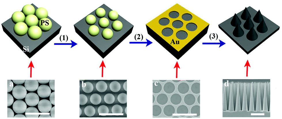 | ||
| Fig. 1 Schematic for fabricating the nanocone array and the corresponding SEM images. The scale bar represents 1 μm. | ||
MaCE includes electrochemical and chemical processes.19–21 It is well accepted that oxidant is reduced at the metal surface, holes (h+) are generated and injected into the Si in the area where it is covered by metal. Thus the Si is oxidized by h+ and dissolved by HF, which results in a vertical etching. When the generated h+ cannot be consumed completely at the interface between Si and metal,13,22 the redundant h+ will diffuse to the area without metal, leading to a lateral etching and roughness on the top surface of the structure, as presented in Fig. 2. The tilt angle of nanostructures depends on the ratio of vertical and lateral etching rates, so the composition of the etchant is the most important factor for the tilt angle, including the ratio of oxidant and HF, and their concentrations.
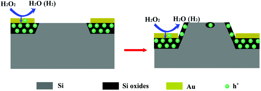 | ||
| Fig. 2 Scheme for the etching mechanism of MaCE. | ||
The etching duration is one of the key factors to determine the morphology of the structure, so we investigated the effect of the etching duration on the tilt angle of the Si nanostructures firstly. The etchant we used in this work includes H2O2 as oxidant, C2H5OH as solvent, and HF for dissolving the oxide layer. The SEM images of the nanocones, the correlation of the etching duration and the tilt angle as well as the height of the nanocones are shown in Fig. S1.† The tilt angle is nearly constant upon extending the etching duration in the same etchant, while the height of the nanocones increases linearly. This means that the etching duration can not affect the etching rate and the tilt angle.
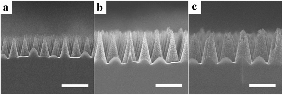
Then, the effect of the volume ratio of H2O2 to HF on the tilt angle was investigated. The effect of the volume ratio of H2O2 to HF on the tilt angle of the nanocones was studied by keeping the volume ratio of (H2O2 + HF):C2H5OH constant at 1:5. The details of the etchant composition and etching duration are presented in Table S1.† The volume of H2O2 increases from 0.65 ml to 2 ml, and the volume of HF decreases from 3.35 ml to 2 ml, correspondingly. As presented in Fig. 3, the tilt angle decreases from 88.6° to 69.2° when the volume ratio of H2O2 to HF increases from 0.19 to 1. For a given structure period, the maximum height of the nanocones depends on the tilt angle. This means that the maximum height increases with the increase of the structure period and tilt angle. For a given etching duration, the height depends on the vertical etching rate when it is less than the maximum. The correlations of the vertical and lateral etching rates with the volume ratio of H2O2 to HF are shown in Fig. 3h. It can be observed that the lateral etching rate gradually increases with increasing the volume ratio of H2O2 to HF, except when it is 1. With a constant volume ratio of (H2O2 + HF):C2H5OH, the concentration of H2O2 increases on increasing the volume ratio of H2O2 to HF, but the concentration of HF decreases. The higher concentration of H2O2 causes more h+ generation and diffusion to the side wall, which increases the lateral etching rate. However, the lower concentration of HF decreases the rate of the Si oxides being dissolved on the side wall, therefore, this increased rate of lateral etching is slowed down.
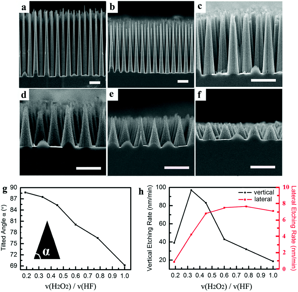 | ||
| Fig. 3 SEM images of the nanocone arrays with tilt angles of (a) 88.6°, (b) 87.5°, (c) 85.3°, (d) 80.1°, (e) 76.5° and (f) 69.2°. (g) Correlation of the tilt angle and the volume ratio of H2O2 to HF. (h) Correlation of the vertical and lateral etching rates with the volume ratio of H2O2 to HF. The scale bars in (a)–(f) are 1 μm. | ||
When the volume ratio of H2O2 to HF increases to 1.67, the whole Si surface is oxidized, but the exposed Si oxide is dissolved faster by HF than that covered with gold film, which leads to the formation of some rough nanopits instead of nanocones, as shown in Fig. S2.† The vertical etching rate depends on the concentrations of H2O2 and HF; either of them in low concentration can result in a lower vertical etching rate. Therefore, the vertical etching rate increases first and then decreases on increasing the volume ratio of H2O2 to HF. The results indicate that the higher volume ratio of H2O2 to HF leads to a smaller tilt angle.
Then we investigate the impact of the concentration of H2O2 and HF on the tilt angle. Keeping the volume ratio of H2O2 to HF constant at 0.33, the concentrations of H2O2 and HF were changed by varying the volume ratio of (H2O2 + HF):C2H5OH. The detailed etchant composition and etching duration are listed in Table S2.† As presented in Fig. 4, when the volume ratio of (H2O2 + HF):C2H5OH decreases from 0.27 to 0.08, the tilt angle decreases from 87.3° to 76.3° (Fig. 4g), and the vertical etching rate decreases from 117.0 to 9.1 nm min−1, while the lateral etching rate only decreases from 5.5 to 2.1 nm min−1 (Fig. 4h). The variation in the vertical etching rate is nearly 32 times that of the lateral etching rate. With the decrease of the volume ratio of (H2O2 + HF):C2H5OH, the concentrations of H2O2 and HF are reduced in equal proportion, therefore the rates of H2O2 reduction and h+ injection are slowed down, and the rate of Si oxides being dissolved also becomes slower, so the vertical etching rate is obviously decreased. Theoretically, due to the volume ratio of H2O2 to HF being constant, the lateral etching rate should reduce in equal proportion with the vertical etching rate, and the tilt angle should remain the same. However, the decreasing rate of the lateral etching is less than that of vertical etching, as shown in Fig. 4h. This phenomenon can be understood as follows: when the concentration of HF is lower, the Si oxide covered by gold film should be dissolved slower because the diffusion of HF is limited by the covering. Therefore the lower concentrations of H2O2 and HF result in the decrease of the tilt angle.
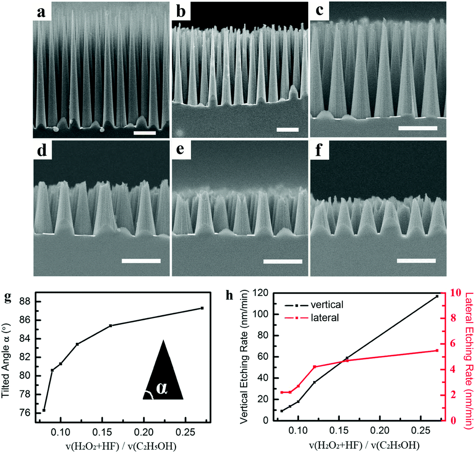 | ||
| Fig. 4 SEM images of nanocone arrays with tilt angles of (a) 87.3°, (b) 85.4°, (c) 83.4°, (d) 81.3°, (e) 80.6° and (f) 76.3°. (g) Correlation of tilt angle and volume ratio of (H2O2 + HF):C2H5OH. (h) Correlation of vertical and lateral etching rates with the volume ratio of (H2O2 + HF):C2H5OH. The scale bars in (a)–(f) are 1 μm. | ||
To test the ability of this method to control the tilt angle, nanocones of the same tilt angle and different period were fabricated using the same etching solution, for which the volume ratio of H2O2:HF:C2H5OH was 1.75:2.25:20. The nanocone arrays are shown in Fig. 5. The tilt angle of the nanocone arrays is 76.5°, and the periods are 450 nm, 600 nm, and 700 nm respectively. This result demonstrates that the tilt angle of the nanocones can be regulated precisely and repeatably.
 | ||
| Fig. 5 SEM images of nanocone arrays with a tilt angle of 76.5° and periods of (a) 450 nm, (b) 600 nm, and (c) 700 nm. The scale bar represents 1 μm. | ||
By varying the composition of the etchant and the etching duration, nanocones with the same height of 2.2 μm and different tilt angles were fabricated. As shown in Fig. 6a–c, the tilt angles of the nanocone arrays are 87.3°, 85.4°, and 83.0°, respectively. The measured total reflectivity of the Si nanocone arrays is presented in Fig. 6d, and the reflectivity decreases with the reduction of tilt angle when the height is the same. When the tilt angle is 83.0°, the average reflectivity is lowered to 1.37% in the 250–1000 nm band. These results indicate that the tilt angle of Si nanocones can be regulated precisely using MaCE in a one-step process over a large area, which results in different optical properties.
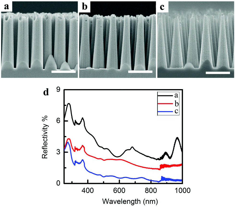 | ||
| Fig. 6 (a–c) SEM images of nanocone arrays with tilt angles of 87.3°, 85.4°, and 83.0° respectively, and the same height of 2.2 μm. The scale bar represents in 1 μm. (d) Total reflectivity of the nanocone arrays shown in (a–c). | ||
Conclusions
In summary, we develop a facile method to regulate the tilt angle of Si nanocones precisely using MaCE in a one-step process, based on the systematic investigation of the formation mechanism of the tilt angle of Si structures. The tilt angles of Si nanocone arrays can be regulated from 69.2° to 88.6° by varying the composition of the etchant. The reflectivity of nanocones decreases with the decrease of the tilt angle when the height of the nanocones is the same. When the height is 2 μm and the tilt angle is 83.0°, the average reflectivity is lowered to 1.37% in the 250–1000 nm band. The Si nanocone arrays with different tilt angles can be fabricated over large areas (as large as 2 cm × 2 cm). This method should be applicable for regulating the tilt angles of other Si structures created using MaCE. The template for MaCE is not limited to metal holes, other metal patterns should be applicable, such as metal stripes, metal dots, metal squares etc. This study may promote the application of MaCE in semiconductor manufacturing.Acknowledgements
This work was supported by the National Natural Science Foundation of China (no. 21273092, 21673096).Notes and references
- M. De Volder and A. J. Hart, Angew. Chem., Int. Ed., 2013, 52, 2412–2425 CrossRef CAS PubMed.
- W. R. Wei, M. L. Tsai, S. T. Ho, S. H. Tai, C. R. Ho, S. H. Tsai, C. W. Liu, R. J. Chung and J. H. He, Nano Lett., 2013, 13, 3658–3663 CrossRef CAS PubMed.
- H. Park, S. Choi, J. P. Lee and S. Park, J. Mater. Chem., 2011, 21, 11996–12000 RSC.
- D. Qi, Z. Liu, M. Yu, Y. Liu, Y. Tang, J. Lv, Y. Li, J. Wei, B. Liedberg, Z. Yu and X. Chen, Adv. Mater., 2015, 27, 3145–3151 CrossRef CAS PubMed.
- I. Zardo, S. Conesa-Boj, S. Estrade, L. Yu, F. Peiro, P. R. I. Cabarrocas, J. R. Morante, J. Arbiol and A. F. I. Morral, Appl. Phys. A: Mater. Sci. Process., 2010, 100, 287–296 CrossRef CAS.
- J. R. Maiolo, B. M. Kayes, M. A. Filler, M. C. Putnam, M. D. Kelzenberg, H. A. Atwater and N. S. Lewis, J. Am. Chem. Soc., 2007, 129, 12346–12347 CrossRef CAS PubMed.
- J. Zhu, Z. F. Yu, G. F. Burkhard, C. M. Hsu, S. T. Connor, Y. Q. Xu, Q. Wang, M. McGehee, S. H. Fan and Y. Cui, Nano Lett., 2009, 9, 279–282 CrossRef CAS PubMed.
- Y. D. Wang, N. Lu, H. B. Xu, G. Shi, M. J. Xu, X. W. Lin, H. B. Li, W. T. Wang, D. P. Qi, Y. Q. Lu and L. F. Chi, Nano Res., 2010, 3, 520–527 CrossRef CAS.
- H. Han, Z. P. Huang and W. Lee, Nano Today, 2014, 9, 271–304 CrossRef CAS.
- D. P. Qi, N. Lu, H. B. Xu, B. J. Yang, C. Y. Huang, M. J. Xu, L. G. Gao, Z. X. Wang and L. F. Chi, Langmuir, 2009, 25, 7769–7772 CrossRef CAS PubMed.
- D. Qi, L. Zheng, X. Cao, Y. Jiang, H. Xu, Y. Zhang, B. Yang, Y. Sun, H. H. Hng, N. Lu, L. Chi and X. Chen, Nanoscale, 2013, 5, 12383–12387 RSC.
- D. H. Lee, Y. Kim, G. S. Doerk, I. Laboriante and R. Maboudian, J. Mater. Chem., 2011, 21, 10359–10363 RSC.
- C. Chartier, S. Bastide and C. Levy-Clement, Electrochim. Acta, 2008, 53, 5509–5516 CrossRef CAS.
- B. Jiang, M. Li, Y. Liang, Y. Bai, D. Song, Y. Li and J. Luo, Nanoscale, 2016, 8, 3085–3092 RSC.
- F. Bai, M. C. Li, R. Huang, Y. F. Li, M. Trevor and K. P. Musselman, RSC Adv., 2014, 4, 1794–1798 RSC.
- F. Bai, M. C. Li, R. Huang, Y. Yu, T. S. Gu, Z. Chen, H. Y. Fan and B. Jiang, J. Nanopart. Res., 2013, 15, 1915–1922 CrossRef.
- H. Lin, H.-Y. Cheung, F. Xiu, F. Wang, S. Yip, N. Han, T. Hung, J. Zhou, J. C. Ho and C.-Y. Wong, J. Mater. Chem. A, 2013, 1, 9942–9946 CAS.
- J. Rybczynski, M. Hilgendorff and M. Giersig, NATO Sci. Ser., II, 2003, 91, 163–172 CAS.
- X. Li and P. W. Bohn, Appl. Phys. Lett., 2000, 77, 2572–2574 CrossRef CAS.
- C. Y. Chen, C. S. Wu, C. J. Chou and T. J. Yen, Adv. Mater., 2008, 20, 3811–3815 CrossRef CAS.
- K. Q. Peng, A. J. Lu, R. Q. Zhang and S. T. Lee, Adv. Funct. Mater., 2008, 18, 3026–3035 CrossRef CAS.
- Z. P. Huang, N. Geyer, P. Werner, J. de Boor and U. Gosele, Adv. Mater., 2011, 23, 285–308 CrossRef CAS PubMed.
Footnote |
| † Electronic supplementary information (ESI) available. See DOI: 10.1039/c6nr08384f |
| This journal is © The Royal Society of Chemistry 2017 |