
Large area growth of vertically aligned luminescent MoS2 nanosheets†
G.
Deokar
*a,
N. S.
Rajput
b,
P.
Vancsó
a,
F.
Ravaux
b,
M.
Jouiad
 *b,
D.
Vignaud
c,
F.
Cecchet
d and
J.-F.
Colomer
a
*b,
D.
Vignaud
c,
F.
Cecchet
d and
J.-F.
Colomer
a
aDepartment of Physics and Research Group on Carbon Nanostructures (CARBONNAGe), University of Namur, 61 Rue de Bruxelles, 5000 Namur, Belgium. E-mail: geetanjali.deokar@unamur.be; mjouiad@masdar.ac.ae
bDepartment of Mechanical and Materials Engineering, Masdar Institute of Science and Technology, 54224, Abu Dhabi, United Arab Emirates
cUniv. Lille, CNRS, UMR 8520 - IEMN, F-59000 Lille, France
dLaboratory of Lasers and Spectroscopy (LLS), Research Centre in Physics of Matter and Radiation (PMR), University of Namur, 61 Rue de Bruxelles, 5000 Namur, Belgium
First published on 18th November 2016
Abstract
Vertically aligned MoS2 nanosheets (NSs) with exposed edges were successfully synthesized over a large area (∼2 cm2). The NSs were grown using an ambient pressure chemical vapor deposition technique via rapid sulfurization of sputter deposited thick molybdenum films. Extensive characterization of the grown MoS2 NSs has been carried out using high resolution scanning and transmission electron microscopy (SEM & TEM). A special care was given to the TEM lamella preparation process by means of a focused ion beam to preserve the NS growth direction. The cross-section TEM measurements revealed the growth of densely packed, vertically aligned and straight MoS2 NSs. Additional characterization techniques such as atomic force microscopy, X-ray photoelectron spectroscopy, Raman spectroscopy, and photoluminescence (PL) were used to evaluate the MoS2 NSs. These studies revealed the high crystallinity and quality of the synthesized NSs. The MoS2 NSs show visible light emission similar to mechanically exfoliated monolayer MoS2 NSs. The striking PL signal comes from the exposed edges as shown by experimental and theoretical calculations. The vertical MoS2 NSs also exhibit a hydrophobic character with a contact angle of 114°. The as-grown MoS2 NSs would be highly useful in the development of catalysis, nano-optoelectronics, gas-sensing and bio-sensing device applications.
Introduction
MX2 (M = Mo, W, etc., X = S, Se, etc.) belongs to the transition metal dichalcogenide (TMD) family, which have a layered structure.1 These TMD materials show properties ranging from metallic, semiconducting to superconducting.1 The interaction between the atoms within the plane is covalent and stronger than the interaction between the atoms residing on different planes, which is of van der Waals interaction type and it is relatively weak. Due to these anisotropic interactions along and between the planes, the electronic, physical, and chemical properties are also anisotropic,1 which give rise to interesting mechanical,2 electrical,3,4 electro-chemical,5 optical,6,7 and catalytic properties.5,8 MoS2 has been a focus of study for applications, such as hydrodesulphurization catalysis,9 hydrogen evolution reaction,10,11 lithium batteries,12,13 photocatalysis,14,15 sensors16,17 and field emission.18 MoS2 possesses good electrical conductivity and can emit light,19 opening possible applications such as photodetectors20 and optoelectronic devices.21 It can also be integrated with other two-dimensional, flexible, and transparent materials.22Owing to its excellent properties and great application potential, extensive research has been carried out to develop various methods to synthesize nanosized MoS2.5,8,23 Along with the high crystalline quality, specific morphology, and application performance, high yield and easy fabrication are also the main factors to be considered for developing a methodology to obtain nanoscale materials. A low cost technique to obtain high-quality mono- to few-layer MoS2 is mechanical exfoliation.19 However, this technique has its own limitation to produce controllable large area growth with a definite number of layers. It is therefore more suitable for fundamental research and proof-of-concept device fabrication. Using chemical exfoliation of MoS2 produces rather low quality MoS2 nanosheets (NSs), compared to mechanical exfoliation,24 which are good for certain applications such as sensors.25 On the other hand, the chemical vapor deposition (CVD) technique has shown promise to generate high-quality MoS2 layers with a scalable size, controllable thickness, and excellent electronic properties.26,27 CVD is also a fairly reliable straightforward technique to obtain various morphologies of MoS2 such as nano-particles,2 nano-tubes,28 nano-wires,29 nano-spirals30 and vertical NSs.31 Vertical MoS2 NSs with both a large specific surface area and sharp, active edges could be used for innovative applications in various areas such as catalysts,31,32 sensors, and field emitters.32 Moreover, the vertically grown structures have shown super-hydrophobic behavior33 and are interesting for self-cleaning application.34
Recently, a CVD-based technique to synthesize vertical MoS2 NSs by sulfurization of MoO3 powder32,35 or e-beam coated Mo films was reported.16,31 It has been demonstrated that the vertical MoS2 NSs grown using low-pressure CVD have great potential for hydrogen evolution reaction (HER),36 gas sensing,16 and water disinfection37 applications. The heterogeneous distribution of the starting material (MoO3 powder) leads to randomly distributed nanosheets with limited control on the thickness and height of NSs.32,35 On the other hand, an Mo film with a definite defined thickness as a starting material could be used to control the MoS2 NS height.31,37,38 However, vertical NS growth using Mo films ≥10 nm thickness and the in-depth growth have been less investigated so far. The present work involves the growth of MoS2 NSs by rapid sulfurization of sputter coated thick Mo (10–300 nm) films using ambient pressure (AP) – CVD. Also the use of sputter coated films is rather more economical compared to that of the e-beam deposited Mo films reported previously and low pressure CVD.16,31 This is an important step towards realization of the large scale production of MoS2 NSs. We have used several characterization techniques, in order to gain greater insight into the growth and characteristics of the as-grown NSs. By extensive cross-section TEM measurements the in-depth growth of nanosheets was studied. We have confirmed that high-crystalline quality, vertically aligned straight MoS2 NSs having properties such as visible light emission and hydrophobicity can be successfully synthesized. Based on our experimental results, a brief growth mechanism was also discussed. The as-grown MoS2 NSs could provide interesting and innovative application opportunities in the fields of nano-optoelectronics, catalysis and sensing.
Experimental
Material synthesis
A sputter-deposited Mo film on a Si (001) substrate was used as a starting material. The Mo film thickness was varied over the 10–300 nm range. A Mo (99.95%, Kurt J. LESKER™) target was used for direct current bias sputtering to deposit Mo films using a homemade sputter deposition system. Ar (purity 99.9995%) gas was used for the sputtering. The Mo film thickness was monitored and controlled using a quartz crystal microbalance mounted in the deposition system. The S powder (99.5%) purchased from Alfa Aesar™ was used without any further purification. The Mo film samples were set downstream to the Ar (purity 99.9995%) flow at a distance of about 2–5 mm from the S source. The quartz tube was first flushed for one hour to remove oxygen using a 0.725 l min−1 Ar flow. Subsequently, the Mo film samples were subjected to sulfurization at 850 °C for 30 min under a constant Ar flow at atmospheric pressure (flow rate – 0.725 l min−1). The NS growth parameters such as the substrate temperature (850 °C), Ar gas flow (0.725 l min−1), S powder quantity (150–300 mg), and synthesis duration (30 min) were adapted from our previously reported NS growth technique.35 Afterward, the furnace was cooled down naturally to room temperature.Physical characterization and computational methods
The sample morphology was observed using a scanning electron microscope (SEM) (JEOL 7500F, operating voltage - 3 kV). For selected samples, in order to obtain high resolution SEM images and to fabricate transmission electron microscopy (TEM) lamellas, a dual focused ion beam (FIB) system (FEI™ Helios NanoLab™ 650) was used. This dual system is equipped with the Elstar™ monochromator Schottky field emission SEM (FE-SEM) technology and a versatile Tomahawk ion column. Elemental composition analysis was performed using energy dispersive spectroscopy (EDS) from EDAX™. TEM lamellas were prepared using a standard FIB process described elsewhere.39 The topography and roughness of the sample surface were characterized by atomic force microscopy (AFM). AFM images were recorded using a Nanoscope III, Bruker™ in tapping-mode.Compositional analyses were performed using X-ray photoelectron spectroscopy (XPS) in a Thermo Fisher Scientific™ K-alpha spectrometer. The spectra were recorded at constant pass energy (150 eV for survey; 20 eV for high resolution spectra). The experiments were performed using a 250 μm diameter X-ray spot. The Mo 3d and S 3p core level signal shapes were analyzed as a set of doublets separated by a well-defined binding energy scale (3.1 and 1 eV, respectively), position and width. These high-resolution spectra were fitted to Gaussian–Lorentzian line-shapes using a Shirley background.
The quality and optical properties of the MoS2 NSs were examined using Raman spectroscopy photoluminescence (PL) and UV-visible spectroscopy. The Raman and PL spectra were recorded using a Horiba™ micro-Raman confocal microscopy system (Lab-RAM). A 473 nm excitation laser line with a low laser excitation power (1 mW) was used for spectra acquisition. The Raman and PL emission were collected by the same objective and dispersed by a 300 lines per mm grating. The typical integration times were 30 s. PL mapping was performed using a laser power of 5 mW, at a 150 lines per mm grating and an accumulation time of 10 s per point. All the measurements were performed at room temperature and in ambient air.
We performed density functional theory (DFT) calculations using the VASP simulation package40 to investigate the electronic properties of the bulk 2-H MoS2. Exchange–correlation effects were taken into account in the framework of the generalized gradient approximation (GGA) by the Perdew–Burke–Ernzerhof (PBE) functional.41 Projector augmented wave (PAW) pseudo-potentials42 were used and the kinetic energy cut-off for the plane wave expansion was 500 eV. The geometry of the atomic positions was relaxed using the conjugate-gradient method until the forces of the atoms were reduced to 0.01 eV Å−1, and the Brillouin-zone was sampled using an 8 × 8 × 4 Monkhorst–Pack mesh.
Static contact angle (CA) measurements were performed with a Dataphysics OCA 35 apparatus, at room temperature, in ambient air, with 0.5 μl droplets of deionized water.
Results and discussion
Scanning electron and atomic force microscopy results
The SEM images collected at different magnifications for the as-deposited 300 nm Mo film and the sulfurized Mo film (with initial thicknesses of 300 and 50 nm) using 300 mg of S powder are presented in Fig. 1. Henceforth, the sulfurized Mo film is denoted as the S–Mo film. The as-deposited Mo film surface and the cross-section (Fig. 1(a)) appear rather smooth. On the other hand, on the 300 nm (Fig. 1(b) and (c)) and 50 nm (Fig. 1(f) and (g)) sulfurized Mo films with 300 mg of S powder at 850 °C for 30 min (named sample-1 and sample-2 respectively), crystals with sizes ranging from a few hundred nanometers to a few microns and NSs with a uniform size of a few tens of nanometers are formed. The crystals appear to have many facets in both samples. The larger nanocrystals formed on sample-2 than on sample-1 might be a result of aggregation of two or more crystals. The presence of MoS2 nanosheets underneath these crystals as well as some embedded MoS2 flakes in them was observed by HR-TEM (presented later), supporting this argument. An EDS map-scan presented in Fig. S1 (see the ESI†) gives the elemental composition for sample-2. Both Mo and S are present in the mapped area as highlighted by the EDS map with an O present mainly in the crystal area. It indicates the presence of an Mo oxide mainly in the crystal region. Similar results were also observed for sample-1 (not shown). The SEM cross-sectional images of sample-1 and sample-2 are shown in Fig. 1(d) and (e) respectively. Two distinct layers were observed for sample-1 (thick S–Mo film). In-depth cross-section TEM investigations are presented later to further understand the nature and structure of the layers as an effect of the Mo film sulfurization. For both samples, an increase in film thickness compared to the initial Mo film thickness was observed (Fig. 1(d) & (e)). This is ascribed to S incorporation and MoS2 formation. It can be easily noticed that the crystal density could be controlled effectively by changing the Mo film thickness and S powder quantity (Fig. S2†). As shown in Fig. S2,† a higher coverage of NSs was indeed observed for lower Mo film thickness (10 nm) sulfurization (with S powder quantity 300 mg).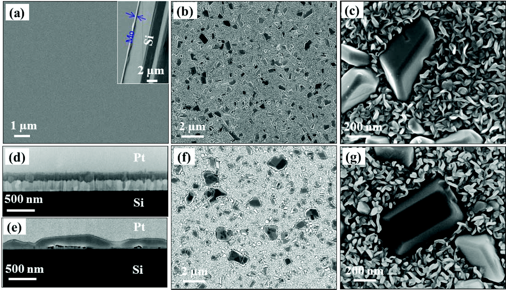 | ||
| Fig. 1 (a) SEM imaging results for a sputter deposited Mo film and in the insert, the corresponding cross-section. In (b), (c) and, (d) for a 300 nm Mo film sulfurized at 850 °C with 300 mg of S powder for 30 min: plane-view low and high-resolution images and a cross-section SEM image, respectively. For a 50 nm Mo film sulfurized with the same parameters: (e), (f), (g) with a cross-section, plane-view low and high resolution SEM images, respectively. | ||
Additionally, the NS thickness and topography were investigated using AFM imaging as displayed in Fig. S3.† The AFM images recorded on 3 × 3 μm2 and 500 × 500 nm2 for sample-1 (Fig. S3(a) and (b)†) and sample-2 (Fig. S3(d) and (e)†) confirm the formation of micron-sized crystals and nanosized NSs, which can be correlated with the SEM data (Fig. 1). The measured thicknesses of NSs are in the range of 20–50 nm (the section profiles (Fig. S3(c) and (f)†)) on both samples with the NSs twice in length for sample-1 compared to sample-2. One can clearly see that the NSs are relatively less densely packed for the thin S–Mo film (sample-2) than that of the thick S–Mo film (sample-1). The root mean square (RMS) surface roughness recorded on 500 × 500 nm2 is of 9 and 11 nm for 300 and 50 nm S–Mo film samples, respectively. Thus the NS growth introduces a much higher roughness compared to the as-deposited film (the RMS surface roughness for the 300 and 50 nm Mo films was 3.2 and 0.4 nm respectively). These results clearly indicate the significant effect of the initial Mo film thickness on the NS length, density and sample surface roughness. High resolution 300 × 300 nm2 topography and phase images for the 50 nm S–Mo film sample are shown in Fig. S3(g) and (h),† respectively. The phase (Fig. S3(h)†) provides well-defined details of sizes, borders, and shapes of all NSs, independent of their Z-position from the substrate.
Indeed, the as-grown NSs are more densely packed compared to those grown using a hydrothermal method43 or using a CVD technique and MoO3 powder as an initial material.32,35
Chemical composition analysis
The chemical nature of the as-deposited and sulfurized Mo film was studied using XPS (Fig. 2). The survey scans for non-sulfurized and sulfurized 10 nm Mo films are displayed in Fig. 2(a). It can be noticed that the O content in the as-deposited Mo film is significantly higher than in the sulfurized Mo film. For the as-deposited Mo film, the deconvoluted peaks of the Mo 3d and O 1s core level are presented in Fig. 2(b) and (c). Two doublet peaks in the Mo 3d core level at the binding energies of 228.2 (Mo 3d5/2) and 231.5 (Mo 3d3/2) eV corresponding to the elemental Mo metal were observed.44 In addition to the metallic Mo, the presence of three component peaks corresponding to different oxidation states (IV, V and, VI) of Mo bonded to oxygen was also observed. The assigned binding energies of Mo 3d5/2 species associated with Mo(IV), Mo(V), and Mo(VI) states are centered at 229.3, 231.5 and 232.8 eV respectively.45 This implies that the surface oxidation of the Mo film occurred during deposition and/or storage in air. In the high-resolution O 1s core level XPS spectra (Fig. 2(c)) of the Mo film, the two oxygen species were assigned to O2− and OH− with binding energies centered at 530.9 and 531.5 eV, respectively, with the main O2− contribution component corresponding to molybdenum oxide phases.44,46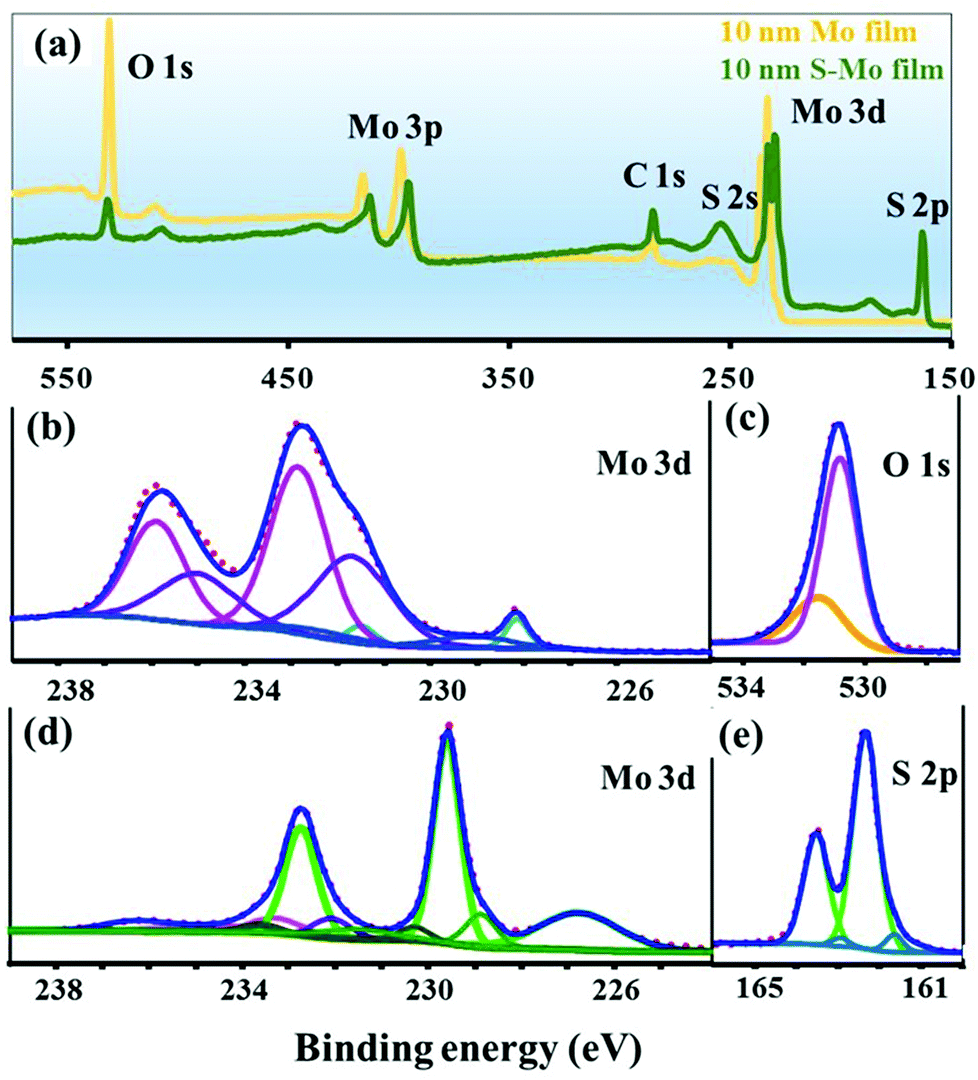 | ||
| Fig. 2 XPS spectra: (binding energy (eV) vs. counts (arbitrary unit) plots): (a) survey spectra for the as-deposited 10 nm Mo film un-sulfurized and the sulfurized one (at 850 °C with 150 mg of S powder for 30 min). In (b) and (c) Mo 3d and O 1s core level spectra and their decomposition for the 10 nm un-sulfurized Mo film. In (d) and (e) Mo 3d and S 2p core level spectra and their decomposition for the sulfurized 10 nm Mo film. In panels (b) to (e) the doublet peaks and component peaks corresponding to the same phases are marked with the same color. | ||
In the survey scan (Fig. 2(a)), S peaks can also be noticed in the sulfurized Mo film, indicating the incorporation of S in the Mo film. The sulfurized 10 nm Mo film Mo 3d and S 2p core level spectra and its decomposition are displayed in Fig. 2(d) and (e) respectively. As shown in Fig. 2(d), the major peaks for Mo 3d5/2 (and Mo 3d3/2) are found to be located at 229.6 (and 232.7) eV, respectively, indicating the prominent presence of the MoS2 phase on the sample surface.47 Moreover, the S 2s peak observed at a binding energy of 226.7 eV confirms the MoS2 formation.11 A small portion of the Mo 3d5/2 and Mo 3d3/2 doublet peaks observed at the lower binding energies of 228.8 and 232.0 eV in the Mo 3d core level spectrum could be attributed to MoS or S-depleted MoS2 species.48 Besides the MoS2 phase, the Mo(IV) and Mo(V) oxidation states of Mo (bonded to oxygen), respectively, as in the case of the as-deposited Mo film were also detected (Fig. 2(b) and (d)). A small signal with the Mo 3d5/2 peak at 233.2 eV might be due to MoOx (with x ≤ 3) species.45,49 The Mo oxide phases detected by XPS could be present mainly in the crystals, as shown in the EDS map-scan (Fig. S1†). A significantly lower signal of the Mo oxide phases in the S–Mo film (Fig. 2(d)) compared to the Mo-film (Fig. 2(b)) indicates an effective reduction of Mo oxide by sulfurization. The S 2p core level spectrum (Fig. 2(e)) for the sulfurized film was fitted with three components. The dominant doublet peaks at 162.3 and 163.3 eV corresponding to the S 2p3/2 and S 2p1/2 orbital, respectively, of divalent sulfide ions (S2−), are attributed to MoS2.47 Consistent with the Mo 3d core level spectra, the small intensity component of the S 2p3/2 and S 2p1/2 peaks seen in the S 2p core level spectra at the lower binding energies of 161.6 and 162.9 eV could be associated with MoS or S-depleted MoS2 species.48 No doublet peaks are present at higher binding energies (163–164.3 eV), indicating no polysulfide of Mo associated with the disulfide ligand formation during the sulfurization process.45
Structural characterization
The in-depth nanosheet growth for two sulfurized samples with an initial Mo film thickness of 300 and 50 nm was studied by cross-section TEM measurements. Fig. 3(a) shows a low magnification TEM image of the cross-section of sample-1 (300 nm S–Mo film). The micrograph of Fig. 3(a) clearly shows two different regions: on the Si substrate, a first zone labeled R1 corresponds to an incompletely sulfurized polycrystalline Mo region followed by a crystalline MoS2 region (R2). A thin amorphous layer of ∼3 nm thickness is also observed just above the Si substrate (not shown). This could be the native Si oxide layer. This is understandable because we have used an Si substrate without using any HF treatment prior to Mo film deposition. Fig. 3(b) shows a high angle annular dark field scanning TEM (HAADF-STEM) image obtained from the top end of the R2 region revealing the vertically oriented layered NS. This sharp edge terminated NS has an interlayer separation of 0.62 nm corresponding to the (002) plane of 2H-MoS2.50 The NS exposed edges with dangling bonds could play an important role in catalysis reactions (for example – hydrodesulfurization).32,50 It should be noted that the nanosheets grown here having the height of a few hundreds of nanometers are much longer than those reported previously by Cho et al.16 or Kong et al.31Fig. 3(c) shows an HRTEM image from the R2 region (Fig. 3(a)). Fig. 3(d) and (e) corresponding to the two areas marked with pink and orange squares respectively in Fig. 3(c) show the lattice parameter measurement using an HRTEM micrograph and the zone axis matching with the atomic arrangement of crystalline MoS2. The fast Fourier transform (FFT) patterns corresponding to Fig. 3(d) and (e) are given in Fig. 3(f) and (g), respectively. The patterns (Fig. 3(d) and (f)), match with the crystal structure of MoS2 ([001] zone axis) with a unit cell parameter of 0.3 nm, whereas Fig. 3(e) and (g) highlight the multi-layered structure of the material along the [110] zone axis. An interlayer distance of 0.5 nm and a Mo atom spacing of 0.24 nm are extracted from Fig. 3(e). This indicates the presence of differently oriented MoS2 grains deeper in the R2 region.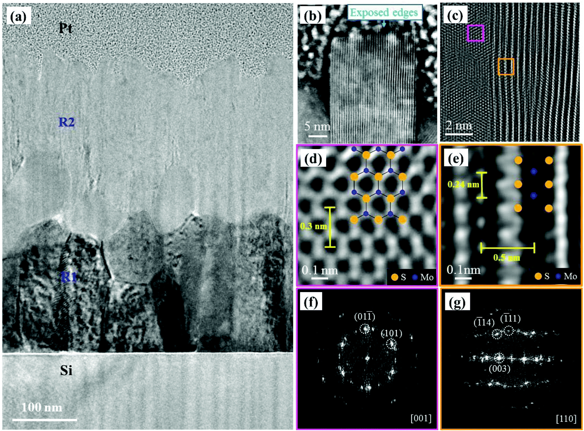 | ||
| Fig. 3 TEM images of the 300 nm S–Mo film sample: (a) low magnification TEM image. (b) STEM-HAADF image showing the MoS2 layers near the interface of the Pt layer and the R2 region. (c) HRTEM image from the middle of the R2 region. (d) Filtered enlargement of the pink square in (c), highlighting the MoS2 crystal along the [001]-zone axis. The inserts show the crystal structure of the specimen and the unit cell parameter. (e) Filtered enlargement of the orange square in (c) highlighting the MoS2 crystal along the [110] zone axis. The inserts show the crystal structure of the specimen, the interlayer spacing and the inter-atomic spacing. (f) and (g) show the FFT of (d) and (e), respectively. | ||
Additionally, we have studied NS growth by cross-sectional TEM for relatively thinner sulfurized Mo films (i.e. 50 nm). The TEM results for sample-2 are presented in Fig. 4. In order to understand the nature of the crystals observed in the SEM images (refer to Fig. 1), we have purposely analyzed the NSs in the vicinity of the crystals by cross-sectional TEM imaging. Unlike sample-1, three main regions were observed (Fig. 4(a)) in sample-2:
(1) Region A shows the growth of the vertically aligned layers of crystalline MoS2 NSs (Fig. 4(a) & (d)). A thin native Si oxide layer of ∼5 nm was observed at the interface of NSs and the Si substrate in this sample as well. As shown in Fig. 4(d)–(f), MoS2 grows straight-up immediately above this silica layer leading to very thin and vertically well aligned MoS2 structures. Similar to sample-1, edge terminated vertical MoS2 NSs can be seen from Fig. 4(e) (area marked by a green rectangle in Fig. 4(d)). Moreover, an HRTEM image of another area from the middle portion of region A is presented in Fig. 4(f). The structural analysis from the red square region is shown in Fig. 4(g). An interlayer distance of 0.62 nm and an interatomic spacing of 0.28 nm between two Mo atoms were found, which corresponds to the (002) oriented crystal planes of the 2H-MoS2 structure.50 The FFT obtained from the vertical NS region (Fig. 4(f)) is given in the inset of Fig. 4(g). This indicates that the zone axis is [110].
(2) Region B1 (the same as B2) also consists of vertical, edge terminated MoS2 NS layers as is clearly seen in Fig. 4(b) and (c). These NSs are found to have the same nature as the ones in region A, except that their growth occurred below the crystals (C1 (the same as C2) region).
(3) The C1 (the same as C2) region (thickness from 200 to 250 nm) appears to be 2 to 3 times thicker than region A. A zoomed-in image of the C1 region is shown in Fig. 4(h). In this region, nanocrystalline flakes are observed to be embedded within a crystalline matrix. As shown in Fig. 4(i) (zoomed-in area corresponding to the pink square in Fig. 4(h)), the MoS2 nano-flake with an interlayer distance of 0.62 nm and a Mo interatomic distance of 0.27 nm are found.50 A zoom in on the yellow-square area (Fig. 4(h)) is shown in Fig. 4(j). Further FFT analysis (Fig. 4(k)) indicates that the matrix has a bcc structure with a [001] zone axis. It is ascribed to crystalline Mo. Thus, it seems that the crystals correspond to unreacted Mo with some 2H-MoS2 flakes embedded in it.
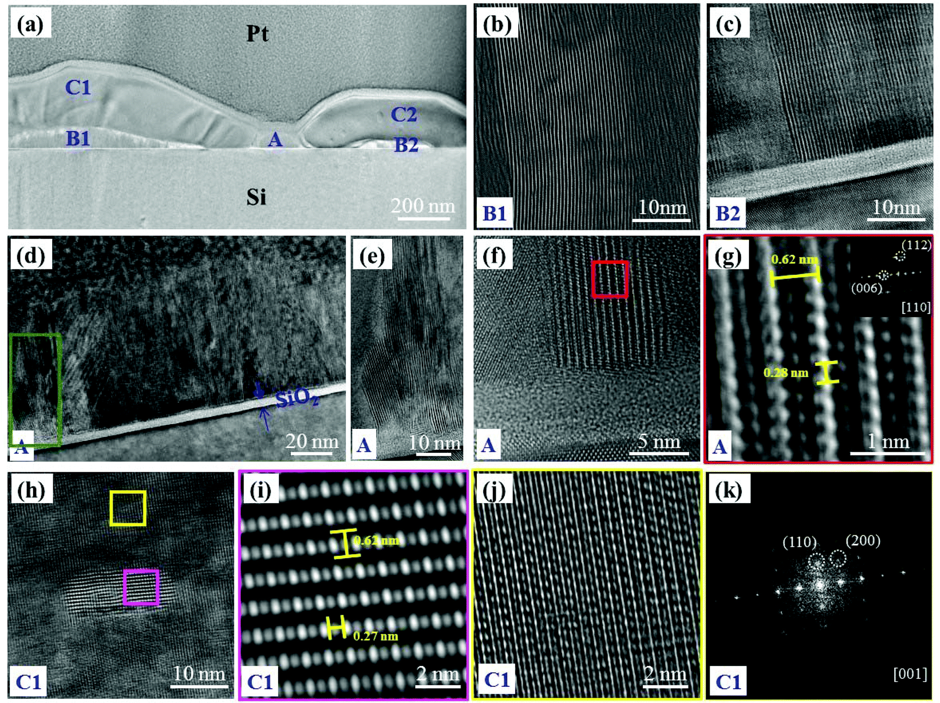 | ||
| Fig. 4 TEM images the 50 nm S–Mo film sample: low magnification TEM image. (b) and (c) Enlargements of the B1 and B2 regions in (a), respectively. (d) TEM image of the A region. (e) Enlargement of the green square in (d), highlighting the exposed edge structure of the A region. (f) HRTEM of the A region. (g) Filtered enlargement of the red square in (f), highlighting the MoS2 crystal in the [110] zone axis. The inserts show the interlayer spacing, the inter atomic spacing, and the FFT of the image. (h) HRTEM image of the C1 region, highlighting the presence of MoS2 nano-flakes embedded in a crystalline Mo matrix. (i) Enlargement of the pink square in (h), highlighting the crystal structure of the MoS2 nano-flake in the [110] direction. The insert shows the interlayer and interatomic spacing. (j) Enlargement of the yellow square in (h), and (k) the FFT. | ||
For the same amount of S powder used for sulfurization, we observed that full sulfurization over the depth (in the crystal-free area) occurred for sample-2 (Fig. 3 & 4) and not for sample-1. During sulfurization, the S vapor diffuses into the Mo film and converts it into Mo sulfide.31,51 Indeed, the chemical conversion (Mo to MoS2) occurs much faster than the diffusion of S vapor through the film, thereby making S diffusion as the NS growth rate-limiting parameter. Due to structural anisotropy, the rate of S diffusion is much faster across the layer than into the layers, resulting in vertically oriented structures.31 Along-with the NSs, not fully sulfurized Mo crystals (Fig. 4) and Mo oxide (Fig. 3) phases were observed indicating a partial sulfurization of the starting material. This could be due to the sputter deposited and thicker Mo film used as a starting material for sulfurization compared to the thin e-beam deposited film used elsewhere.31,52
Raman, PL and UV-visible spectroscopic experiments and theoretical explanation
The Raman and PL spectra are shown in Fig. 5 for MoS2 NSs grown by sulfurization of Mo films with 300 or 50 nm initial thickness (sample-1 and sample-2). As shown in Fig. 5(a), the presence of the E12g (in-plane Raman mode) at ∼382 cm−1 and the A1g mode (out-of-plane Raman mode) at ∼405 cm−1 clearly demonstrates the formation of 2H-MoS2.53 The frequency difference (Δf) between the E12g and A1g modes can be reliably used to count the number of MoS2 layers.54,55 The Δf value observed for the two samples (Fig. 5(a)) is ∼27 cm−1. This indicates the presence of five or more layers of MoS2 in the NSs.54 The PL spectra for the same samples recorded in the NS area are shown in Fig. 5(b). Two transitions denoted as mode A and mode B (Fig. 5(b)) appearing at 1.82 and 1.95 eV (in the visible region) are observed for the two samples. Interestingly, the PL feature observed here occurs at a similar energy position to that of the direct band-gap monolayer MoS219 indicating the growth of NSs with comparable optical quality to that of the monolayer MoS2. The PL spectrum for sample-2 exhibits a stronger PL intensity compared to that of sample-1. As seen from the SEM, AFM and TEM results, the NS thickness is comparable for both samples while the length and height are different, which might be responsible for lower PL signals. Fig. 5(c) shows an optical image of sample-2 over which a PL map was recorded. In the optical image, the darker areas correspond to Mo crystal growth, and the plane areas correspond to NSs as confirmed by SEM imaging (Fig. 1). The A exciton energy (EA) peak position variation in the recorded PL map area is displayed in Fig. 5(d). Over the mapped area, the observed EA position variation is only 0.06 (1.77–1.83) eV. Bulk MoS2 is an indirect band-gap semiconductor and generally optically inactive, while the MoS2 monolayer exhibits a direct band-gap and shows a strong PL signal varying from 1.8 to 1.9 eV.6,7,19 Bilayer MoS2 NSs show an indirect band-gap-like nature with an additional transition peak present at 1.6 eV in addition to the A and B modes.7 It has been shown previously that more than seven horizontally stacked MoS2 NSs (thickness >5 nm) do not show any luminescence.6 Interestingly, in spite of being multilayers (with thickness ≥20 nm), the NSs grown on the 50 nm S–Mo film give a prominent PL signal comparable to the one observed for monolayer MoS2.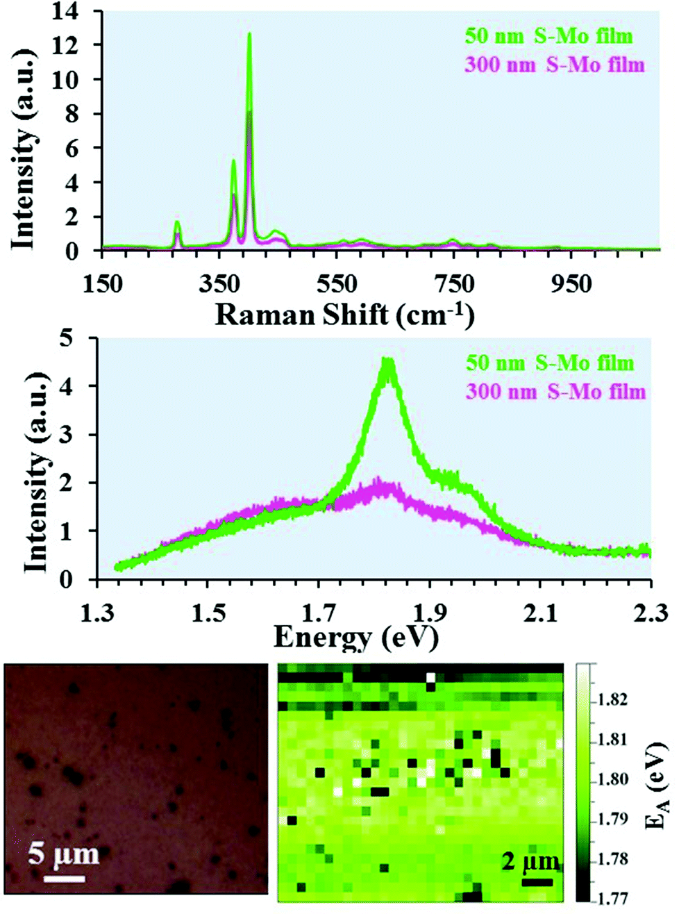 | ||
| Fig. 5 (a) and (b) Raman scattering and PL of MoS2 nanosheets grown by sulfurization of a Mo film using 300 mg of S powder at 850 °C for 30 min, respectively. (c) Optical image of the 50 nm S–Mo film sample over which a PL map was recorded. (d) The exciton A peak energy position (EA) map. | ||
In order to understand the similarities between the PL results of our MoS2 NSs and monolayer MoS2, we have applied density functional theory calculations and the zone-folding approach56 to describe the electronic states of the NSs. Fig. 6(a) shows the bulk MoS2 band structure at the PBE level with an indirect band gap (0.94 eV).57 It is worth noting that PBE calculations underestimate the band gap of single layer MoS2 (1.67 eV)58,59 compared to the measured optical gap (1.8–1.9 eV). Besides the indirect band gap in the bulk, a direct-gap transition (1.6 eV) similar to monolayer MoS2 appears at the K point of the Brillouin zone between the maximum of split valence bands and the minimum of the conduction band (Fig. 6(a)). Our calculations predict a slightly larger value of the direct gap (less than 0.1 eV) at the K point in the monolayer compared to the bulk, in good agreement with previous theoretical60 and experimental findings.61 To approach the electronic properties of our finite-size MoS2 NSs, we applied the zone-folding scheme by using the calculated band structure of bulk MoS2. The height of our NSs is indeed too large (a few hundreds of nanometers) for performing ribbon-like calculations. We modeled the NSs with finite heights regarding the stable molybdenum terminated (10![[1 with combining macron]](https://www.rsc.org/images/entities/char_0031_0304.gif) 0) edge62 and infinite lengths. In Fig. 6(b) we show the zone-folded one-dimensional (1D) band structure of the modeled MoS2 NS with 6.6 nm height. We note that our method neglects the proper edge states,63 however, this, approximation remains appropriate as long as the number of bulk states dominates the few number of edge states. Our main result is that the indirect and direct band gaps of the bulk MoS2 remain in the MoS2 NS band structure. Moreover, this property is independent of the heights of the NSs. Therefore, our MoS2 NSs are indirect-gap materials, but they also have a direct-gap transition with similar values to those in the bulk and slightly less than in monolayer MoS2. As we mentioned earlier PL in bulk MoS2 has a negligible quantum yield (QY).6 However, the exposed edges of MoS2 NSs as observed by TEM measurements (Fig. 3 and 4) of the vertically grown NSs might have a significant role in the observed PL emission. It has been shown experimentally that the edges can increase the PL signal.64–66 Because the Raman and PL intensities are equally affected by the local electric fields, both the Raman and the PL signals could be enhanced simultaneously in case the edges of the MoS2 NSs induced a surface enhanced Raman spectroscopy (SERS)-like effect. To support this explanation, we measured the intensity of the Raman A1g mode in our MoS2 NSs which we compared to bulk MoS2 values. The measured ratio of the A1g mode of NSs to bulk has been found one order of magnitude higher showing a remarkable enhancement in the case of MoS2 NSs (see Fig. S4†). Therefore, we can conclude that the enhanced PL signal from our grown NSs mostly comes from their edges that induce a SERS-like effect responsible for a significant QY increase of the bulk-direct-gap transition that becomes visible even in the presence of the indirect band gap. The fact that (1) the slightly lower position of the PL signal of our NSs (1.82 eV) compared to the monolayer (1.88 eV), and (2) the increased PL intensity in the case of sample-2 where the surface-to-bulk ratio is higher compared to sample-1 due to the shorter length of NSs directly support our hypothesis about the edge effect.
0) edge62 and infinite lengths. In Fig. 6(b) we show the zone-folded one-dimensional (1D) band structure of the modeled MoS2 NS with 6.6 nm height. We note that our method neglects the proper edge states,63 however, this, approximation remains appropriate as long as the number of bulk states dominates the few number of edge states. Our main result is that the indirect and direct band gaps of the bulk MoS2 remain in the MoS2 NS band structure. Moreover, this property is independent of the heights of the NSs. Therefore, our MoS2 NSs are indirect-gap materials, but they also have a direct-gap transition with similar values to those in the bulk and slightly less than in monolayer MoS2. As we mentioned earlier PL in bulk MoS2 has a negligible quantum yield (QY).6 However, the exposed edges of MoS2 NSs as observed by TEM measurements (Fig. 3 and 4) of the vertically grown NSs might have a significant role in the observed PL emission. It has been shown experimentally that the edges can increase the PL signal.64–66 Because the Raman and PL intensities are equally affected by the local electric fields, both the Raman and the PL signals could be enhanced simultaneously in case the edges of the MoS2 NSs induced a surface enhanced Raman spectroscopy (SERS)-like effect. To support this explanation, we measured the intensity of the Raman A1g mode in our MoS2 NSs which we compared to bulk MoS2 values. The measured ratio of the A1g mode of NSs to bulk has been found one order of magnitude higher showing a remarkable enhancement in the case of MoS2 NSs (see Fig. S4†). Therefore, we can conclude that the enhanced PL signal from our grown NSs mostly comes from their edges that induce a SERS-like effect responsible for a significant QY increase of the bulk-direct-gap transition that becomes visible even in the presence of the indirect band gap. The fact that (1) the slightly lower position of the PL signal of our NSs (1.82 eV) compared to the monolayer (1.88 eV), and (2) the increased PL intensity in the case of sample-2 where the surface-to-bulk ratio is higher compared to sample-1 due to the shorter length of NSs directly support our hypothesis about the edge effect.
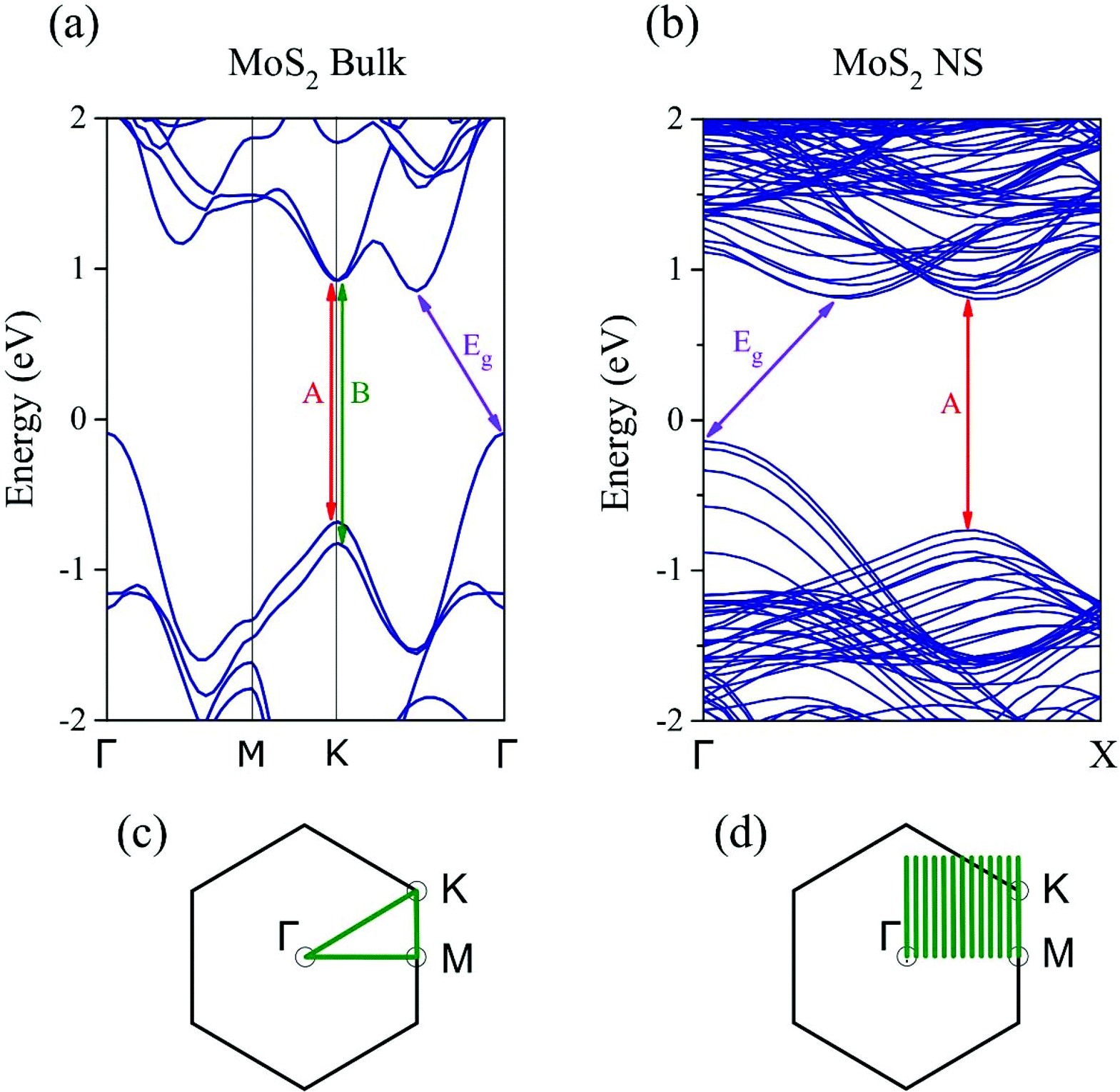 | ||
| Fig. 6 (a), (b) Electronic band structure for the MoS2 bulk and NS, respectively. Direct-gap transitions at the K-point lead to A- and B-type excitons. (c), (d) Projected two dimensional Brillouin zone for the bulk MoS2. High symmetry lines are shown for the bulk, while the parallel equidistant lines represent the lines along which the wave vector is discretized due to the finite size of the NS. | ||
Finally, we would like to note that the PL intensity could be influenced by other external factors such as doping,67,68 strain69,70 or excitation laser power.71 In order to reveal further mechanisms which may affect the measured PL intensity for our MoS2 NSs, more detailed experimental as well as theoretical studies are necessary.
Wettability behavior
A surface is classified as hydrophobic or hydrophilic (repelling water) depending upon the CA which the water droplet forms on the considered sample surface. If the CA lies between 90 and 150°, the surface is hydrophobic and it is hydrophilic if the CA lies between 0° and 90°. It has been shown previously that the horizontally stacked mono- or few-layer and bulk MoS2 have a hydrophilic (CA < 90°) character.72,73 We have determined the wetting properties of deionized water on the as-deposited and sulfurized Mo films. For the un-sulfurized 50 nm Mo film (RMS roughness 0.4 nm as from AFM) and the MoS2 NSs grown by sulfurization of the 50 nm Mo film (RMS roughness 11), the CAs of a water droplet were found to be 59° and 114°, respectively (Fig. 7). The CA depends on several factors, such as the surface energy, the roughness, the surface preparation, and the surface cleanliness.74 The hydrophobic properties of any surface can be enhanced by introducing micro- and nano-roughness and/or by the creation of air pockets.74 The as-deposited Mo film shows a CA similar to the ones previously reported Mo films on glass (56.7°–69.7°).75 On the other hand, the as-grown MoS2 NSs show a much higher CA than the previously reported horizontally stacked MoS2 NSs (<90°).72,73 This is probably due to the growth of distinctive vertical MoS2 NSs having nanoscale thickness and roughness (see the Scanning electron and atomic force microscopy results section). In addition, the hydrophobicity could be further improved by Mo crystal-free vertical NS growth.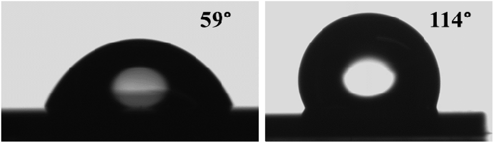 | ||
| Fig. 7 Wettability measurements: typical photographs showing water droplets on (a) the 50 nm unsulfurized Mo and (b) 50 nm S–Mo films, respectively. | ||
Potential applications of the as-grown MoS2 NSs
Both the exposed surface area and active site density are very important for providing a large amount of active sites for catalysis and sensor applications. It has been shown that the adsorption energy and active sites are lower for horizontal MoS2 nanosheets than that of the vertical one and thus having fivefold higher gas sensitivity.16 The as-grown densely packed nanosheets, over a large area, could be efficiently useful for hydrodesulphurization catalysis,9 HER,10,11 sensors,16,17 lithium batteries,12,13 water cleaning37 and photocatalysis14,15 applications thanks to their high density of exposed edges and hundreds of nanometers height. To minimize electronic transfer limitations in Li batteries and water cleaning devices, highly conductive supports are required. The as-grown NSs could be transferred on excellent electrical conducting substrates (example – Cu, graphene) by adopting the chemical transfer technique used to transfer graphene grown on Ni/SiO2/Si substrates.76 The CVD grown well-defined thin nanosheets with a thickness of 20–50 nm show PL signals in the visible region which makes them a potential candidate for the fabrication of photodetectors20 and optoelectronic devices.21 Additionally, the observed hydrophobic nature of the MoS2 NSs combined with the luminescence properties could trigger bio-sensing device applications.77Conclusions
2H-MoS2 NSs with a thickness of 20–50 nm were fabricated by rapid sulfurization of Mo films using the AP-CVD technique with multiple qualities: (1) use of a simple synthesis technique that can be easily scaled up; (2) large-area growth of densely packed vertically aligned straight NSs; (3) edge terminated NSs with a height of a few hundreds of nanometers; (4) PL in the visible range; (5) hydrophobic behavior. This was evidenced from the results of various complementary microscopy and spectroscopic characterization techniques, including SEM, AFM, TEM, Raman, PL, and UV-visible spectroscopy, as well as wettability measurements. The most striking result is the fact that the as-grown NSs exhibited PL at a similar energy position to monolayer MoS2 with excellent intensity. Using DFT simulations, we demonstrated that this result originated from the edges of the NSs due to the increased quantum yield of the bulk-direct-gap transition of MoS2. Along with the nanosized MoS2 NSs, micron-sized crystal formation was also observed. In the future studies, we will address crystal free NS growth. The as-grown vertically aligned luminescent MoS2 NSs with a uniform thickness and height could find potential applications in flat-panel displays. Moreover, the as-produced NSs with a high hydrophobic character could also be a potential material for bio-sensing applications. More generally, this work can provide a route toward the low cost scalable growth of TMD NSs for their use as a potential material for electronics, optoelectronics, and bio-medical device fabrication.Acknowledgements
G. Deokar is thankful to P. Louette for his help in the XPS measurements and Prof. B. Lian-Su for allowing wettability measurements. We are grateful to N. Reckinger and Ph. Lambin for careful proof-reading of this manuscript. This work was financially supported by the University of Namur grant. This research used resources of the Electron Microscopy Service of University of Namur and Electron Microscopy and Clean Room facilities of Masdar Institute. These services are the members of ‘Plateformes Technologiques Morphologie – Imagerie and SIAM’, respectively. This research has also used computing resources of the ‘platform technologigue de calcul intensif (PTCI)’ supported by the FRS-FNRS (connection no. 2.4520.11). F. Cecchet and J.-F. Colomer are research associates of FRS-FNRS. The research leading to these results received partial funding from the European Union Seventh Framework Program under the grant agreement no. 604391 Graphene Flagship.References
- J. A. Wilson and A. D. Yoffe, Adv. Phys., 1969, 18, 193–335 CrossRef CAS.
- L. Rapoport, N. Fleischerb and R. Tenne, J. Mater. Chem. A, 2005, 15, 1782–1788 RSC.
- B. W. Baugher, H. O. Churchill, Y. Yang and P. Jarillo-Herrero, Nano Lett., 2013, 13, 4212–4216 CrossRef CAS PubMed.
- T. Y. Kim, M. Amani, G. H. Ahn, Y. Song, A. Javey, S. Chung and T. Lee, ACS Nano, 2016, 10, 2819–2826 CrossRef CAS PubMed.
- G. Zhang, H. Liu, J. Qu and J. Li, Energy Environ. Sci., 2016, 9, 1190–1209 Search PubMed.
- G. Eda, H. Yamaguchi, D. Voiry, T. Fujita, M. Chen and M. Chhowalla, Nano Lett., 2011, 11, 5111–5116 CrossRef CAS PubMed.
- K. F. Mak, C. Lee, J. Hone, J. Shan and T. F. Heinz, Phys. Rev. Lett., 2010, 105, 136805 CrossRef PubMed.
- M. K. Santanu Das, J.-w. Lee and W. Choi, Crit. Rev. Solid State Mater. Sci., 2014, 39, 231–252 CrossRef.
- J.-F. Paul and E. Payen, J. Phys. Chem. B, 2003, 107, 4057–4064 CrossRef CAS.
- C. B. Ma, X. Qi, B. Chen, S. Bao, Z. Yin, X. J. Wu, Z. Luo, J. Wei, H. L. Zhang and H. Zhang, Nanoscale, 2014, 6, 5624–5629 RSC.
- R. D. Nikam, A. Y. Lu, P. A. Sonawane, U. R. Kumar, K. Yadav, L. J. Li and Y. T. Chen, ACS Appl. Mater. Interfaces, 2015, 7, 23328–23335 Search PubMed.
- S. Ding, D. Zhang, J. S. Chen and X. W. Lou, Nanoscale, 2012, 4, 95–98 RSC.
- Z. L. Tyler Stephenson, B. Olsenab and D. Mitlin, Energy Environ. Sci., 2014, 7, 209–231 Search PubMed.
- Y. Li, Y. L. Li, C. M. Araujo, W. Luo and R. Ahujaab, Catal. Sci. Technol., 2013, 3, 2214–2220 Search PubMed.
- W. Zhou, Z. Yin, Y. Du, X. Huang, Z. Zeng, Z. Fan, H. Liu, J. Wang and H. Zhang, Small, 2013, 9, 140–147 CrossRef CAS PubMed.
- S. Y. Cho, S. J. Kim, Y. Lee, J. S. Kim, W. B. Jung, H. W. Yoo, J. Kim and H. T. Jung, ACS Nano, 2015, 9, 9314–9321 CrossRef PubMed.
- C. Zhu, Z. Zeng, H. Li, F. Li, C. Fan and H. Zhang, J. Am. Chem. Soc., 2013, 135, 5998–6001 CrossRef CAS PubMed.
- H. Fu, K. Yu, H. Li, J. Li, B. Guo, Y. Tan, C. Song and Z. Zhu, Dalton Trans., 2015, 44, 1664–1672 RSC.
- A. Splendiani, L. Sun, Y. Zhang, T. Li, J. Kim, C. Y. Chim, G. Galli and F. Wang, Nano Lett., 2010, 10, 1271–1275 CrossRef CAS PubMed.
- J. Pak, J. Jang, K. Cho, T. Y. Kim, J. K. Kim, Y. Song, W. K. Hong, M. Min, H. Lee and T. Lee, Nanoscale, 2015, 7, 18780–18788 RSC.
- L. Britnell, R. M. Ribeiro, A. Eckmann, R. Jalil, B. D. Belle, A. Mishchenko, Y. J. Kim, R. V. Gorbachev, T. Georgiou, S. V. Morozov, A. N. Grigorenko, A. K. Geim, C. Casiraghi, A. H. Castro Neto and K. S. Novoselov, Science, 2013, 340, 1311–1314 CrossRef CAS PubMed.
- H. Wang, L. Yu, Y. H. Lee, Y. Shi, A. Hsu, M. L. Chin, L. J. Li, M. Dubey, J. Kong and T. Palacios, Nano Lett., 2012, 12, 4674–4680 CrossRef CAS PubMed.
- Y. Shi, H. Li and L. J. Li, Chem. Soc. Rev., 2014, 44, 2744–2756 RSC.
- Y. Wang, J. Z. Ou, S. Balendhran, A. F. Chrimes, M. Mortazavi, D. D. Yao, M. R. Field, K. Latham, V. Bansal, J. R. Friend, S. Zhuiykov, N. V. Medhekar, M. S. Strano and K. Kalantar-Zadeh, ACS Nano, 2013, 7, 10083–10093 CrossRef CAS PubMed.
- W. Zhang, P. Zhang, Z. Su and G. Wei, Nanoscale, 2015, 7, 18364–18378 RSC.
- K. Kang, S. Xie, L. Huang, Y. Han, P. Y. Huang, K. F. Mak, C. J. Kim, D. Muller and J. Park, Nature, 2015, 520, 656–660 CrossRef CAS PubMed.
- C. M. Orofeo, S. Suzuki, Y. Sekine and H. Hibino, Appl. Phys. Lett., 2014, 105, 083112 CrossRef.
- J. Chen, S. L. Li, Q. Xu and K. Tanaka, Chem. Commun., 2002, 1722–1723 RSC.
- S. Han, C. Yuan, X. Luo, Y. Cao, T. Yu, Y. Yang, Q. Li and S. Yeb, RSC Adv., 2015, 5, 68283–68286 RSC.
- L. Zhang, K. Liu, A. B. Wong, J. Kim, X. Hong, C. Liu, T. Cao, S. G. Louie, F. Wang and P. Yang, Nano Lett., 2014, 14, 6418–6423 CrossRef CAS PubMed.
- D. Kong, H. Wang, J. J. Cha, M. Pasta, K. J. Koski, J. Yao and Y. Cui, Nano Lett., 2013, 13, 1341–1347 CrossRef CAS PubMed.
- H. Li, H. Wu, S. Yuan and H. Qian, Sci. Rep., 2016, 6, 21171 CrossRef CAS PubMed.
- J. Yu, L. Qin, Y. Hao, S. Kuang, X. Bai, Y. M. Chong, W. Zhang and E. Wang, ACS Nano, 2010, 4, 414–422 CrossRef CAS PubMed.
- P. Gould, Mater. Today, 2003, 6, 44–48 Search PubMed.
- G. Deokar, D. Vignaud, R. Arenal, P. Louette and J. F. Colomer, Nanotechnology, 2016, 27, 075604 CrossRef CAS PubMed.
- H. Wang, Q. Zhang, H. Yao, Z. Liang, H. W. Lee, P. C. Hsu, G. Zheng and Y. Cui, Nano Lett., 2014, 14, 7138–7144 CrossRef CAS PubMed.
- C. Liu, D. Kong, P. C. Hsu, H. Yuan, H. W. Lee, Y. Liu, H. Wang, S. Wang, K. Yan, D. Lin, P. A. Maraccini, K. M. Parker, A. B. Boehm and Y. Cui, Nat. Nanotechnol., 2016 DOI:10.1038/nnano.2016.138.
- Y. Zhao, L. Kuai, Y. Liu, P. Wang, H. Arandiyan, S. Cao, J. Zhang, F. Li, Q. Wang, B. Geng and H. Sun, Sci. Rep., 2015, 5, 8722 CrossRef CAS PubMed.
- N. S. Rajput, S.-G. Kim, J. B. Chou, J. Abed, J. Viegas and M. Jouiad, MRS Adv., 2016, 1(13), 825–830 CrossRef CAS.
- G. Kresse and J. Hafner, Phys. Rev. B: Condens. Matter, 1994, 49, 14251–14269 CrossRef CAS.
- J. P. Perdew, K. Burke and M. Ernzerhof, Phys. Rev. Lett., 1996, 77, 3865–3868 CrossRef CAS PubMed.
- P. E. Blochl, Phys. Rev. B: Condens. Matter, 1994, 50, 17953–17979 CrossRef.
- J. M. Wu, W. E. Chang, Y. T. Chang and C. K. Chang, Adv. Mater., 2016, 28, 3718–3725 CrossRef CAS PubMed.
- J.-H. Bihn, P. Juyun and Y.-C. kang, J. Korean Phys. Soc., 2011, 58, 509–514 CrossRef CAS.
- P. A. Spevack and N. S. Mcintyre, J. Phys. Chem., 1993, 97, 11031–11036 CrossRef CAS.
- P. A. Spevack and N. S. Mcintyre, J. Phys. Chem., 1993, 97, 11020–11030 CrossRef CAS.
- P. Qina, G. Fang, W. Ke, F. Cheng, Q. Zheng, J. Wan, H. Lei and X. Zhao, J. Mater. Chem. A, 2014, 2, 2742–2756 RSC.
- P. P. Wang, H. Sun, Y. Ji, W. Li and X. Wang, Adv. Mater., 2014, 26, 964–969 CrossRef CAS PubMed.
- J. A. Anderson, A. Guerrero and J. L. G. Fierro, Top. Catal., 1994, 1, 123–136 CrossRef CAS.
- J. Deng, W. Yuan, P. Ren, Y. Wang, D. Deng, Z. Zhang and X. Bao, RSC Adv., 2014, 4, 34733 RSC.
- K. Kunimori, K. Tomoji, T. Kondow, T. Onishi and K. Tamaru, Surf. Sci., 1974, 46, 567–576 CrossRef CAS.
- A. J. Cho, K. C. Park and J. Y. Kwon, Nanoscale Res. Lett., 2015, 10, 115 CrossRef PubMed.
- L. Cai, J. He, Q. Liu, T. Yao, L. Chen, W. Yan, F. Hu, Y. Jiang, Y. Zhao, T. Hu, Z. Sun and S. Wei, J. Am. Chem. Soc., 2015, 137, 2622–2627 CrossRef CAS PubMed.
- C. Lee, H. Yan, L. E. Brus, T. F. Heinz, J. Hone and S. Ryu, ACS Nano, 2010, 4, 2695–2700 CrossRef CAS PubMed.
- J.-U. Lee, J. Park, Y.-W. Son and H. Cheong, Nanoscale, 2015, 7, 3229–3236 RSC.
- N. Hamada, S.-I. Sawada and A. Oshiyama, Phys. Rev. Lett., 1992, 68, 1579–1581 CrossRef CAS PubMed.
- H.-P. Komsa and A. V. Krasheninnikov, Phys. Rev. B: Condens. Matter, 2015, 91, 125304 CrossRef.
- Y. Ding, Y. Wang, J. Ni, L. Shi, S. Shi and W. Tang, Physica B, 2011, 406, 2254–2260 CrossRef CAS.
- A. Ramasubramaniam, Phys. Rev. B: Condens. Matter, 2012, 86 Search PubMed.
- A. Kuc, N. Zibouche and T. Heine, Phys. Rev. B: Condens. Matter, 2011, 83, 245213 CrossRef.
- K. F. Mak, C. Lee, J. Hone, J. Shan and T. F. Heinz, Phys. Rev. Lett., 2010, 105 Search PubMed.
- J. V. Lauritsen, J. Kibsgaard, S. Heveg, H. Topsøe, B. S. Clausen, E. Lægsgaard and F. Besenbacher, Nat. Nanotechnol., 2007, 2, 53–58 CrossRef CAS PubMed.
- M. V. Bollinger, J. V. Lauritsen, K. W. Jacobsen, J. K. Nørskov, S. Helveg and F. Besenbacher, Phys. Rev. Lett., 2001, 87, 196803 CrossRef CAS PubMed.
- H. R. Gutierrez, N. Perea-Lopez, A. L. Elias, A. Berkdemir, B. Wang, R. Lv, F. Lopez-Urias, V. H. Crespi, H. Terrones and M. Terrones, Nano Lett., 2013, 13, 3447–3454 CrossRef CAS PubMed.
- H. Nan, Z. Wang, W. Wang, Z. Liang, Y. Lu, Q. Chen, D. He, P. Tan, F. Miao, X. Wang, J. Wang and Z. Ni, ACS Nano, 2014, 8, 5738–5745 CrossRef CAS PubMed.
- M. S. Kim, S. J. Yun, Y. Lee, C. Seo, G. H. Han, K. K. Kim, Y. H. Lee and J. Kim, ACS Nano, 2016, 10, 2399–2405 CrossRef CAS PubMed.
- S. Mouri, Y. Miyauchi and K. Matsuda, Nano Lett., 2013, 13, 5944–5948 CrossRef CAS PubMed.
- K. F. Mak, K. He, C. Lee, G. H. Lee, J. Hone, T. F. Heinz and J. Shan, Nat. Mater., 2013, 12, 207–211 CrossRef CAS PubMed.
- L. Yang, X. Cui, J. Zhang, K. Wang, M. Shen, S. Zeng, S. A. Dayeh, L. Feng and B. Xiang, Sci. Rep., 2014, 4, 5649 CrossRef CAS PubMed.
- C. R. Zhu, G. Wang, B. L. Liu, X. Marie, X. F. Qiao, X. Zhang, X. X. Wu, H. Fan, P. H. Tan, T. amand and B. Urbaszek, Phys. Rev. B: Condens. Matter, 2013, 88, 121301(R) CrossRef.
- V. Senthilkumar, L. C. Tam, Y. S. Kim, Y. Sim, M.-J. Seong and J. I. Jang, Nano Res., 2014, 7, 1759–1768 CrossRef CAS.
- P. K. Chow, E. Singh, B. C. Viana, J. Gao, J. Luo, J. Li, Z. Lin, A. L. Elias, Y. Shi, Z. Wang, M. Terrones and N. Koratkar, ACS Nano, 2015, 9, 3023–3031 CrossRef CAS PubMed.
- A. P. Gaur, S. Sahoo, M. Ahmadi, S. P. Dash, M. J. Guinel and R. S. Katiyar, Nano Lett., 2014, 14, 4314–4321 CrossRef CAS PubMed.
- Y. C. Jung and B. Bhushan, Prog. Mater. Sci., 2011, 56, 1–108 CrossRef.
- I. Tashlykov, A. Turavets and P. Zukowski, Acta Phys. Pol., A, 2013, 123, 840–842 CrossRef CAS.
- A. Reina, X. Jia, J. Ho, D. Nezich, H. Son, V. Bulovic, M. S. Dresselhaus and J. Kong, Nano Lett., 2009, 9, 30–35 CrossRef CAS PubMed.
- J. Lee, P. Dak, Y. Lee, H. Park, W. Choi, M. A. Alam and S. Kim, Sci. Rep., 2014, 4, 7352 CrossRef CAS PubMed.
Footnote |
| † Electronic supplementary information (ESI) available. See DOI: 10.1039/c6nr07965b |
| This journal is © The Royal Society of Chemistry 2017 |