
 Open Access Article
 This Open Access Article is licensed under a Creative Commons Attribution-Non Commercial 3.0 Unported Licence
A classical description of subnanometer resolution by atomic features in metallic structures†
S.
Trautmann
a,
J.
Aizpurua
b,
I.
Götz
a,
A.
Undisz
c,
J.
Dellith
a,
H.
Schneidewind
 a,
M.
Rettenmayr
c and
V.
Deckert
*ad
a,
M.
Rettenmayr
c and
V.
Deckert
*ad
aLeibniz Institute of photonic technology (IPHT), Albert-Einstein-Straße 9, D-07745 Jena, Germany. E-mail: volker.deckert@uni-jena.de
bCentro de Física de Materiales, Centro Mixto CSIC-UPV/EHU and Donostia International Physics Center (DIPC), ES-20018 Donostia-San Sebastián, Spain
cOtto Schott Institute of Materials Research, University of Jena, Löbdergraben 32, D-07743 Jena, Germany
dInstitute of Physical Chemistry and Abbe Center of Photonics, University of Jena, Helmholtzweg 4, D-07743 Jena, Germany
First published on 22nd November 2016
Abstract
Recent experiments have evidenced sub-nanometer resolution in plasmonic-enhanced probe spectroscopy. Such a high resolution cannot be simply explained using the commonly considered radii of metallic nanoparticles on plasmonic probes. In this contribution the effects of defects as small as a single atom found on spherical plasmonic particles acting as probing tips are investigated in connection with the spatial resolution provided. The presence of abundant edge and corner sites with atomic scale dimensions in crystalline metallic nanoparticles is evident from transmission electron microscopy (TEM) images. Electrodynamic calculations based on the Finite Element Method (FEM) are implemented to reveal the impact of the presence of such atomic features in probing tips on the lateral spatial resolution and field localization. Our analysis is developed for three different configurations, and under resonant and non-resonant illumination conditions, respectively. Based on this analysis, the limits of field enhancement, lateral resolution and field confinement in plasmon-enhanced spectroscopy and microscopy are inferred, reaching values below 1 nanometer for reasonable atomic sizes.
Introduction
The usage of nanostructures made of metals as nanoantennas for enhancing optical signals has been exploited in several fields of photochemistry.1,2 Such nanostructures enable collective oscillations from conduction electrons due to the absence of a band gap. These so-called surface plasmons (or localized surface plasmon polaritons) show the ability to enhance the electromagnetic field in the proximity of the nanostructures.3 Several modes can be excited depending on the shape, material, size and surrounding medium of the nanostructures, leading to subwavelength localization and large field enhancements.4,5 Consequently when utilized in applications such as scattering-type near-field scanning optical microscopy (s-NSOM) or tip-enhanced spectroscopies (TERS, TEIRA, etc.) these effects result in a lateral resolution beyond the diffraction limit.6–8In general, such arrangements can be realized by producing nanostructures with sharp edges or with the use of metal–insulator–metal (MIM) configurations (consisting essentially of different combinations of 2 metallic structures of different shapes and approaching an organic layer) which generate a probing cavity.9–13 An improvement regarding resolution can be obtained by further substructuring these near-field probes.14–16
Considering the “crude” dimensions of plasmonic structures, as for instance obtained from SEM, the field confinement in these structures reaches only a few nanometers at best and cannot directly explain the recently experimentally demonstrated lateral resolution below 1 nm.17–21 Additional localization of electromagnetic fields might be related to the presence of much smaller (ultimately down to a single atom) features, usually not considered when describing the morphology of nanostructures in generally applied models. Often, plasmonic structures are approximated by simple shapes described as spheres, ellipsoids or tips with smooth and well defined surfaces.22,23 Realistic models of plasmonic nanostructures, however, need to consider ideally atomic-scale features.24,25 These features are generally unknown (number and specific location of atoms, specific location of defects) and thus render it difficult to build a theoretical model accounting for such effects. In surface-enhanced Raman scattering (SERS), randomly nanoshaped structures were first considered to explain the effect of enhanced fields localized at rough surfaces.26–28 However, these studies did not address the issue of field localization due to the presence of atomic scale features. A novel theoretical investigation of realistic nanostructures was tackled by applying Time-Dependent Density Functional Theory (TDDFT) calculations to Na380 clusters.29 In this study, it was shown that the protruding surface atoms can introduce extra field localization features. Other groups studied near- and far-field effects of anisotropic nanoclusters using TDDFT and have shown similar results.30,31 An experimental indication of field localization due to atomic distributions was also shown by electron-energy loss spectroscopy (EELS) measurements on Ag and Al nanoparticles.32,33 A quite different theoretical approach investigated the structural response of a molecule when a Ag20 cluster was mapped over the entire structure. This approach demonstrated that even without considering any field localization, the lateral resolution based on the spectral response is localized down to sub-molecular features.34
Here, we present a “classical” approach to include atomic scale features on smooth surfaces by dividing the entire nanostructure into a simple base structure with a substructure attached to it. The base structure (e.g. a sphere) defines nanoscale shape-dependent plasmonic modes whereas the substructure mimics a more realistic surface topography of the nanostructure. This approach allows for separately studying the different contributions to the physical mechanisms of potential sub-nm resolution.
We assume the validity of classical electrodynamics to describe the localization and distribution of the local fields, where no chemical effects involving charge transfer at the molecules deposited on the hosting structures are considered, and neither are strong non-local or quantum tunneling effects.35 This approach is particularly relevant for the general TERS case, where a usually dielectric sample is investigated on a dielectric sample holder.
Evidence of atomic scale substructures on plasmonic probes
In order to assess the occurrence and nature of atomic scale substructures of nanoparticles on plasmonic probes as suggested in the theoretical concept, High Resolution Transmission Electron Microscopy (HR-TEM) was carried out on Ag nanoparticles for TERS application using a Jeol JEM-3010. For the preparation, 99.99% pure Ag was thermally evaporated in a high vacuum system onto commercially available AFM tips (Tap190Al-G, Budget Sensors, Bulgaria). The pressure before evaporation was in the lower 10−7 mbar region in order to minimize residual oxygen partial pressure. The deposition of Ag with respect to speed and thickness was controlled by means of a quartz crystal microbalance. The amount of Ag deposited was chosen in order to obtain nanospheres with a diameter of ∼30 nm. For the experimental evaluation, TERS tips were directly observed by TEM using a custom built tip holder (Fig. 1a). However, the exposure to the intense electron beam eventually altered both the shape and the crystallinity of the Ag particles when observed in the high resolution mode. For a minimum particle modification due to the beam/particle interaction, a sufficiently quick dissipation of the beam energy towards the substrate is required. To enhance energy dissipation, Ag was thermally evaporated onto SiO2 membranes coated onto a copper grid as a substrate for TEM (Quantifoil SiO2 at 200 mesh copper grid, Plano, Germany). The SiO2 covered grids provide the same substrate material for generating the Ag nanoparticles as in the case of the Si AFM tips covered by the natural oxide. Compared to TERS tips, the SiO2 membrane, in combination with the copper grid, apparently allowed faster dissipation of energy. Along the edges of the holes in the SiO2 membrane, Ag nanoparticles of sizes similar to those generated at the apex of the TERS tips were formed (Fig. 1b) and were subjected to HR-TEM. The Ag nanoparticles on the flat surfaces of the membrane are considerably larger because the amount of the deposited material depends on the cosine of the tilt angle of the surface. Already at medium TEM resolution, it becomes obvious that, on AFM tips as well as on the edges of the membrane, most of the Ag nanoparticles feature internal interfaces (namely primarily twin and/or grain boundaries). This discovery already substantiates the fact that atomic scale substructures on Ag nanoparticles for plasmonic probes exist. Indeed, Fig. 1c shows a relevant example of a high resolution image where internal interfaces extending to the surface of a single particle are particularly clearly visible. More specifically, a distinct topographical feature (on the order of a single atom) significantly different from an assumed spherical shape can be observed. This resembles a sharp edge (column of atoms) or even a tip at the junction of two edges. | ||
| Fig. 1 Transmission electron microscopy images displaying Ag nanoparticles as deposited (a) onto the apex of a TERS tip and (b) and (c) onto the edge of a SiO2 membrane on a copper grid; (a) and (b): Ag nanoparticles on the TERS tip and the edge of the SiO2 membrane are of comparable size; particles on both types of substrates exhibit internal interfaces; (c): details of an Ag nanoparticle on the SiO2 membrane in high resolution. It can clearly be seen that, particularly at sites where internal interfaces extend to the surface of the particle, atomic scale topological features that significantly alter the local curvature are present. | ||
Computational details
Plasmonic near-field probes generally consist of massive metallic probes, films or the above mentioned deposited nanoparticles.8,36,37 Commonly used materials are Au and Ag; hence, we theoretically investigated both metals to study the most common situations for typical TERS probes, i.e. nanoparticles of ∼20 nm in diameter that aggregate on a template AFM tip. Here, as an approximation, we consider only the foremost nanoparticle and approximate it by a single sphere. This simplified model system captures the essence of the plasmonic nanoscale localization of the field. A Finite Element Method (FEM) in Comsol Multiphysics 4.4 is used to solve Maxwell's equations for stationary problems.38 In this calculation, the constitutive relation for linear materials (σ = 0, μr = 1, where σ and μr are conductivity and relative permeability, respectively) was used. The solution of Maxwell's equations provides the field distribution around the tip that is necessary for the study of field localization and enhancement that we intend to tackle.The model system primarily consists of a smooth spherical nanoparticle as a basic supporting nanostructure. This basic nanostructure was modified by placing a single atomic-scale plasmonic substructure (ASPS) on top of it (see schemes in Fig. 2) to account for the geometries experimentally found (Fig. 1). This substructure was defined as a Gaussian shaped parametric surface that allows for a systematic variation of the ASPS regarding the angle or the depth of the protrusion from the base structure. This approach is useful, because a smooth boundary between the background structure and the ASPS avoids the presence of geometrical singularities.39,40
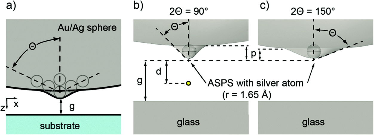 | ||
| Fig. 2 (a) Schematic representation of a spherical nanoparticle base, roughened by a Gaussian shaped atomic scale plasmonic substructure (ASPS). The angle Θ can be associated with a lattice orientation from an atomic feature at the particle surface. (b, c) The protrusion (p) can be controlled via the angle Θ with a constant gap distance (g). The position of the field measurement will be described as the distance from the particle (d) and was varied for specific fields between the nanoparticle and substrate. | ||
To investigate the properties of the commonly used metal–insulator–metal (MIM) nanogap system, including material-dependent features, three different configurations are considered: Ag-particle/glass, Au-particle/glass and a MIM configuration with an Ag nanoparticle above a 20 nm Au layer as the substrate. For all the three configurations, the system response was investigated both under resonant and non-resonant illumination conditions.
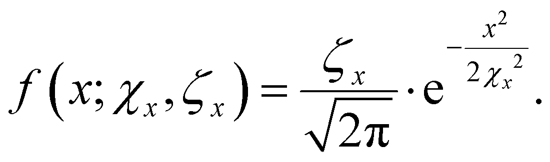
In order to systematically vary the atomic-scale protrusion, a Gaussian function with two parameters (χ and ζ) was used and the actual profile function is expressed as:
 | (1) |
Here χ refers to the parameter that determines the elongation in x and ζ to the respective elongation in z (eqn (2)). For calculating the protrusion, the following atomic radii (Ag = 1.65 Å; Au = 1.74 Å) were used as envelope sizes.41 The elongation parameter ζ was therefore constant for every atomic radius (ζAg = 0.85; ζAu = 0.9) and only χ was varied (Fig. 2b and c) to generate the different angles and protrusions.
In all calculations, the gap distance between the ASPS and the substrate surface was kept constant (g = 1 nm) by moving the base particle in z (Fig. 2b and c). Therefore a tangential smoothing between the particle and the substructure surface was warranted. This constant gap distance ensures comparable excitation of the nanoparticle by the external evanescent field. For investigating the field enhancement, the axial local-field distribution dependence on the distance from the particle (d; see Fig. 2b) and the protrusion size/angle were used.
All calculations were realized in a cubic boundary layer system (700 nm × 700 nm). The side walls were assumed to be formed under periodic boundary conditions with Floquet-periodicity while the top and bottom walls were periodic port boundary layers. The incident p-polarized electromagnetic wave was transmitted via the bottom port boundary layer through a substrate with a constant refractive index (n = 1.52) and an incident angle of 60°. Consequently the field above the substrate boundary is evanescent, a situation that is likely to be faced in any experiment. The relative permittivity of Ag and Au was taken from Johnson and Christy.42 The minimum tetrahedral mesh size used was 0.09 nm.
Results and discussion
Influence of ASPS size on plasmonic resonances
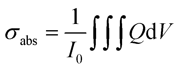
To determine the plasmonic dipole modes and the influence of the ASPS protrusion on the plasmon resonance of the system, the absorption cross section (σabs) was calculated.The latter was determined using the following expression:
 | (2) |
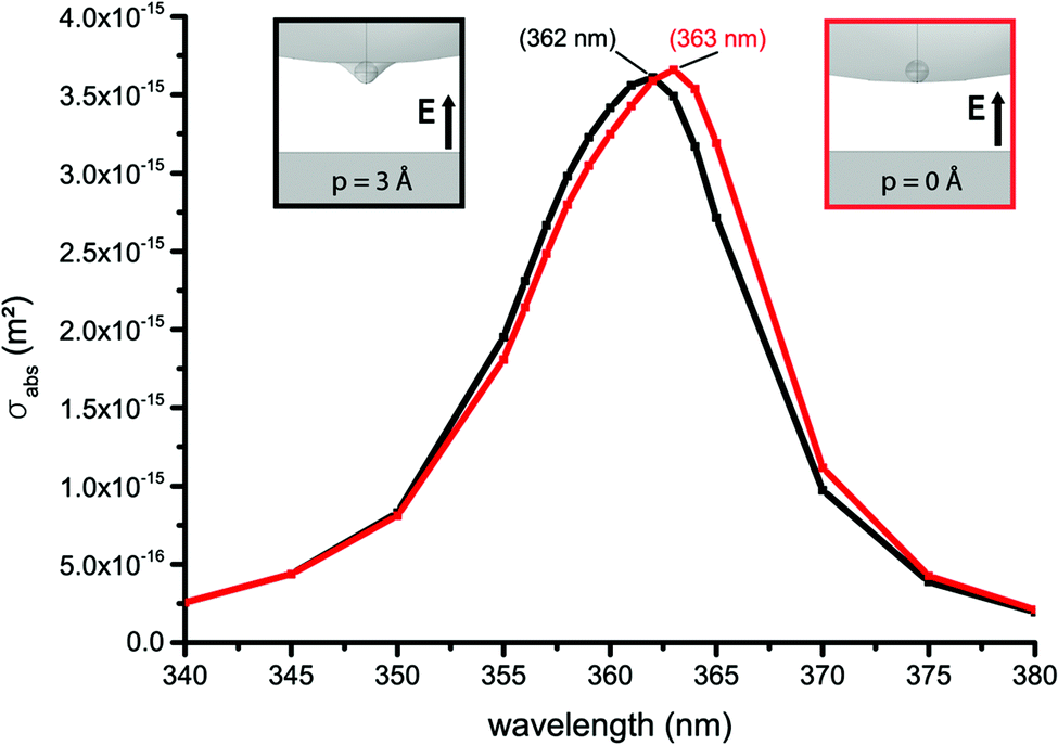 | ||
| Fig. 3 Wavelength dependence of the absorption cross section of a 20 nm Ag nanoparticle with (p = 3 Å, black line) and without atomic protrusion (p = 0 Å, red line). The incident field polarization was perpendicular to the substrate. | ||
Clearly the plasmonic resonance of the particle with an ASPS (p = 3 Å) is blue shifted only by 1 nm with respect to the situation where the nanoparticle shows no substructure (p = 0 Å). The influence on the near-field enhancement will be discussed later.
Enhancement factor and spatial resolution in atomic sub-structures
We now address the relationship of the spatial resolution and of the near-field enhancement with respect to the presence of atomic-sized features on plasmonic structures. For this purpose, we calculated the field distribution for our three model systems (Ag/glass, Au/glass, Ag/Au-layer). In Fig. 4 the local field enhancement factor is mapped for the three geometries under off- and on-resonance conditions. To particularly highlight the effect of the ASPS a special color-coding was used. The color scale was normalized with respect to the maximum enhancement of the base plasmonic nanoparticle (namely a perfect sphere without any substructure). Any additional field enhancement induced by the ASPS above this threshold value is therefore visible as a dark red colored area. The absolute maximum enhancement factor is provided separately on top of each color bar (Fig. 4), and a comparison with the two numbers clearly shows an enhancement due to the ASPS. It is also obvious from Fig. 4 that in all cases the maximum field enhancement is in very close proximity to the ASPS.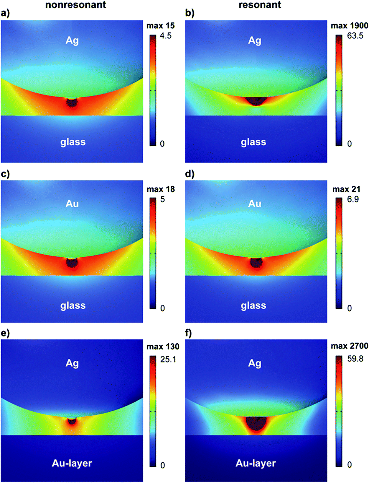 | ||
| Fig. 4 Local induced field enhancement factors for several particle–substrate configurations with a substructure protrusion size of 3 Å. Left column non-resonant, right column resonant enhanced nanoparticle. (a), (b) Ag/glass; (c), (d) Au/glass; (e), (f) Ag/Au-layer configuration with a 20 nm thick Au layer. The color bar was normalized with respect to the particle enhancement without a substructure to show the additional fields associated with the ASPS effect. The maximum value above the color bar is the absolute maximum enhancement factor at the apex. | ||
From the results compiled in Fig. 4, one can conclude that field hotspots originating from ASPS are not prominent for gap separation distances larger than 1 nm. This is in accordance with the study of Trügler et al.27 who showed the small influence of rough nanostructures on the scattered field. However, for small objects or small gap distances (<1 nm), the atomic scale surface topography plays an important role. In such a case, the fields are strongly localized and can be understood as a consequence of an atomistic lightning rod effect.13,29 Such short distances are still beyond the repulsive regime of a chemical bond model. Hence, from a scanning probe point-of-view, these distances are realistic and must be considered when discussing the field intensity versus the tip–sample distance dependence.
For realistic TERS tips, it is difficult to know the exact resonance for the foremost particles at the tip apex. Recent simulations of rough metal films, for instance, revealed the influence of particle spacing on the plasmon resonance and on the field enhancement at the probe apex.43 Here, it is worth highlighting that atomic substructures can also be important for high lateral resolution in TERS, independently of the resonance wavelength.
To study this effect in further detail, calculations of the three situations considered here were performed under off-resonance and on-resonance conditions. For off-resonance situations, the additional field enhancement due to the ASPS is located at the apex of the substructure (dark red area in Fig. 4a, c and e). In the case of an Ag probe over a non-conductive substrate (Fig. 4a and b), the field enhancement is located close to the particle following the underlying plasmonic dipolar distribution, and on-resonance a dramatic field enhancement is found. The resonance behavior for a Au nanoparticle is far less distinct due to the small nanoparticle size and material properties (Fig. 4c and d). Here the resonant and out of resonance cases are similar. In the MIM configuration (Fig. 4e and f) a higher field enhancement can be found compared to the case shown in Fig. 4a, as expected for the so-called gap-mode. In the non-resonant case, the field enhancement is still localized at the ASPS apex but compared to the previous metal-dielectric configuration, (Fig. 4a and c) the typical gap-mode distribution is visible. In the resonant MIM configuration (Fig. 4f) the additional field from the ASPS is even further extended towards the surface.
In order to more clearly visualize the field localization and the field enhancement caused by the ASPS, Fig. 5 shows the axial field distribution at a distance of 3 Å from the ASPS (d; see Fig. 2). The distance between the ASPS and the substrate was kept as 1 nm. The blue line refers to the reference case when the ASPS vanishes in the base structure. This is the classical case and it refers to the field enhancement of a Ag sphere with a 20 nm diameter at a distance of 3 Å from the virtual sample surface. The 7.6 nm FWHM of the field enhancement nicely matches previous results for spherical particles.23 As the ASPS protrudes out of the base structure, a ultra-confined region of extreme field localization emerges on top of the “classical” enhancement curve with a FWHM ∼ 1 nm (Fig. 5a). This additional field localization is primarily situated close to the nanoparticle. As a result the presence of a protrusion like a crystal corner or an atomic scale defect can drastically increase the lateral resolution (FWHM).
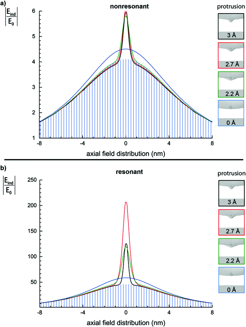 | ||
| Fig. 5 Axial local-field distribution normalized to the incident field amplitude |Eind/E0| for several protrusions (p; see Fig. 2). Here the non-resonant (a) and resonant cases (b) are plotted for a distance from the particle (d) with an ASPS feature progressively protruding from 0 to 3 Å (0 Å, 2.2 Å, 2.7 Å, 3 Å). The axial field distribution clearly shows a peak on top of a baseline background. The broad background is associated with the plasmonic field of the plasmonic base structure and the narrow peak is associated with the ASPS. The respective particle shapes are plotted on the right-hand side inset. The blue bars refer to the field enhancement of a sphere without ASPS d + 3 Å away from the sample, hence, this can be considered as the plain sphere contribution. The substrate was glass, and the particle material was Ag. | ||
To further illustrate the effects associated with the substructure, we present the field enhancement (Fig. 6) and FWHM of the enhancement, which is directly related to the lateral resolution (Fig. 7), for different tip–sample distances and ASPS protrusions (p, Θ), simultaneously.
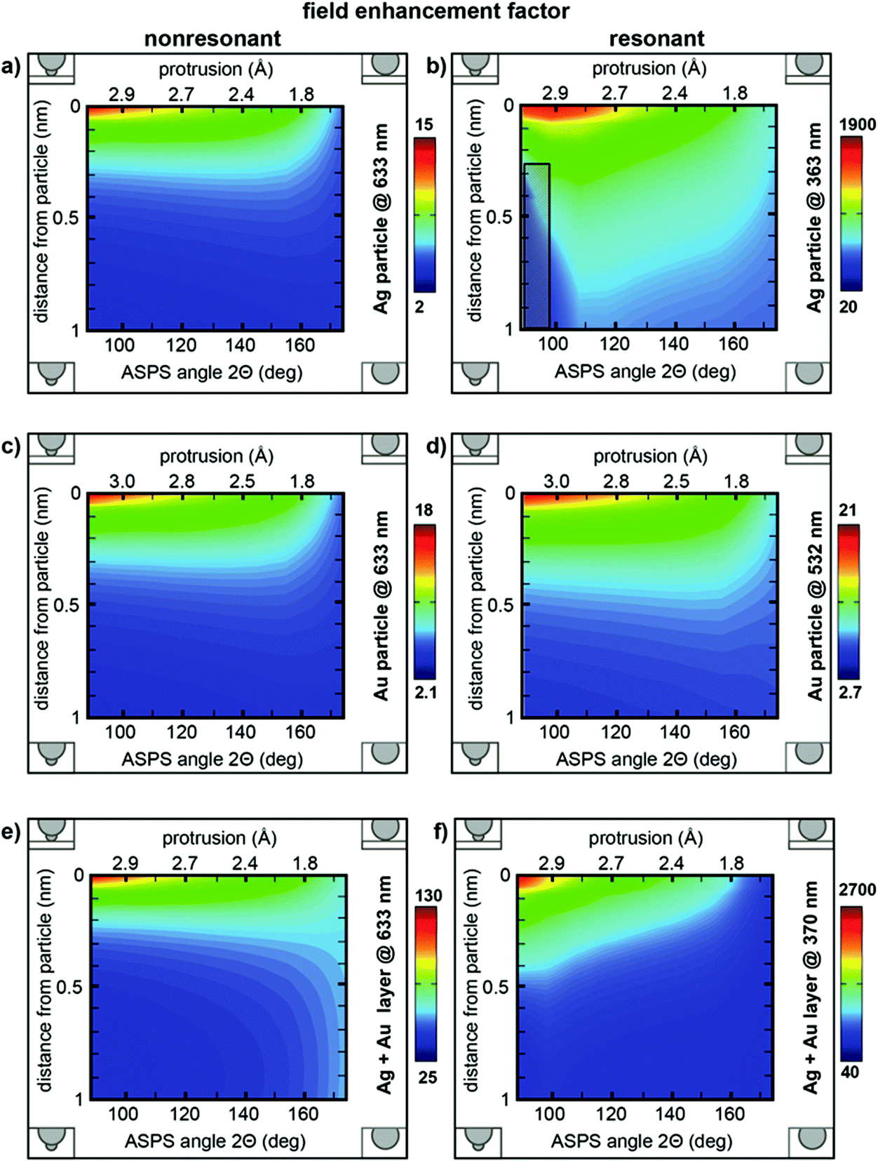 | ||
| Fig. 6 Color maps of the maximum enhancement factor (Eind/E0), with respect to the tip–sample distance and ASPS protrusion/angle. Left column non-resonant, right column resonant enhanced nanoparticle. (a), (b) Ag/glass; (c), (d) Au/glass; (e), (f) Ag/Au-layer configuration with a 20 nm thick Au layer. In (b) a multi-peak area is marked, which is due to an overlap from the broad background that is associated with the plasmonic field of the plasmonic base structure and the narrow peak is associated with the ASPS. Here the most intense peak was selected. The small insets in each figure qualitatively explain the parameters: left side “large” protrusion; right side “protrusion vanished in the base structure”. Top: ASPS just touches the sample; bottom: “large” distance between the ASPS and sample. | ||
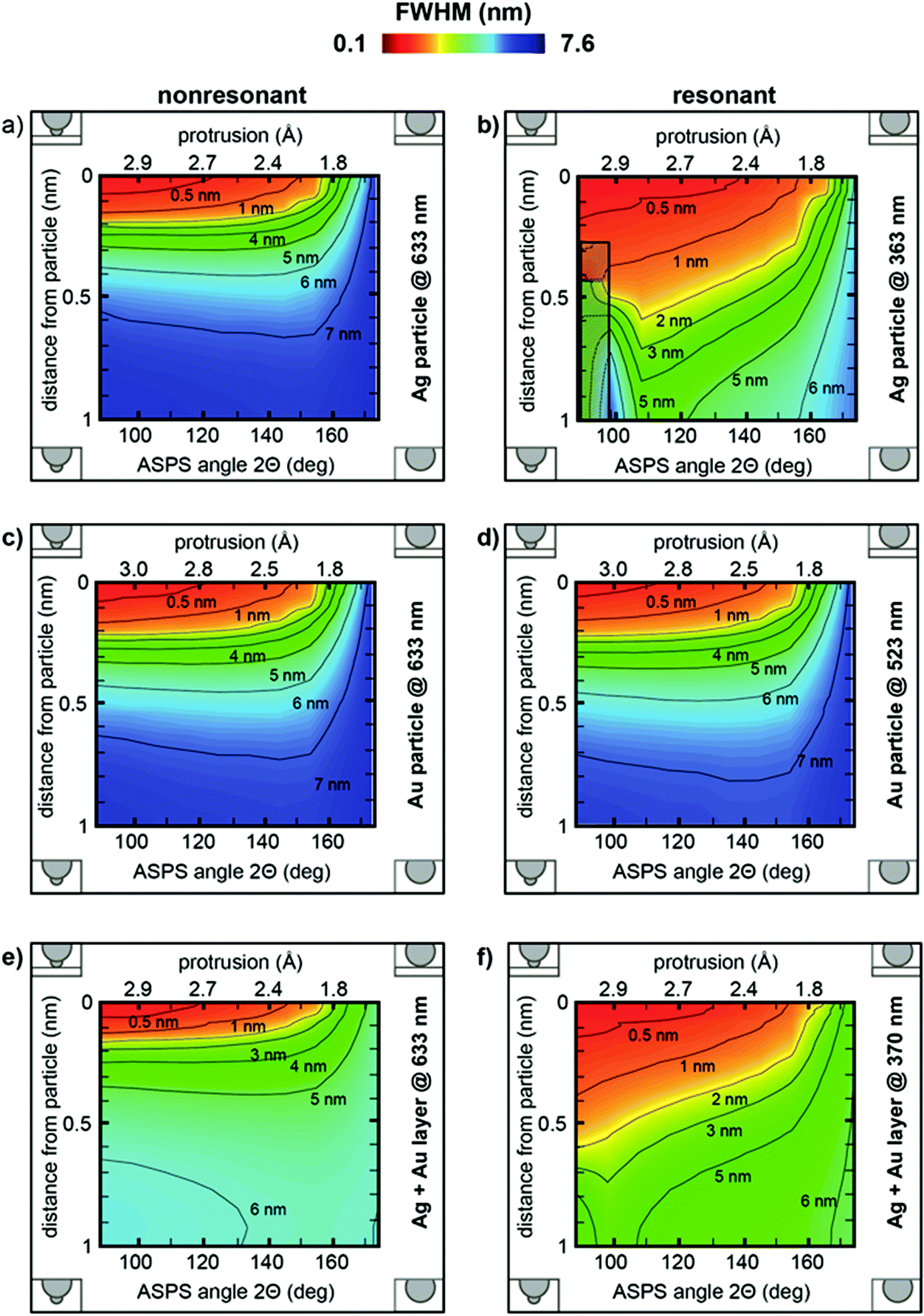 | ||
| Fig. 7 Color maps of the calculated FWHM from the enhanced field (Eind/E0) with respect to the tip–sample distance and ASPS protrusion/angle. Left column non-resonant, right column resonant enhanced nanoparticle. (a), (b) Ag/glass; (c), (d) Au/glass; (e), (f) Ag/Au-layer configuration with a 20 nm thick Au layer. Insets as described for Fig. 5. | ||
Interestingly, for off-resonance enhanced particles and for distances above 4 Å (Fig. 6a, c and e) the maximum enhancement factor is hardly influenced by the ASPS protrusion (3 Å–1.8 Å). Below a distance of 4 Å the enhancement increases and relies on the size of the ASPS protrusion. Under resonant conditions, the enhancement factor is significantly more affected by the protrusion (Fig. 6b and f).
As expected, for a Au probe the resonant case (Fig. 6d) does not substantially differ from the non-resonant case due to the material properties.
The plots in Fig. 7 indicate the dependence of the FWHM on the tip-sample distance d (see Fig. 2b) and the ASPS protrusion. For the resonantly excited Ag particle (Fig. 7b and f), the resolution is clearly higher, even for longer distances, as compared to the non-resonant cases (Fig. 7 left column), which is in accordance with the enhancement factor calculations in Fig. 5.
The marked area in Fig. 6b and 7b represents a region where interferences and charge oscillations of two types of fields between the base particle and the substructure are prominent. This space field distribution makes it particularly difficult to determine a FWHM. Therefore, we neglected this region in our consideration.
A further important aspect, for non-resonantly excited particles (Fig. 7 left column), is that distances from the particle below 2 Å and large protrusions (>2.8 Å) are necessary to get a resolution below 1 nm when just considering the electromagnetic field. As the corresponding protrusion values in these cases are extreme (>2.9 Å), they consequently represent less likely cases and thus the remaining values still cover the most realistic instances.
Based on the calculations, it is interesting to note that apparently the actual protrusion of the defect is less important for enhancement and FWHM under non-resonant conditions. As long as a slight imperfection of the sphere is present it seems to result in an almost uniform and distance independent enhancement. Under resonant conditions the actual parameters of the defect play a much more important role.
As the Raman signal depends roughly on the 4th power of the field amplitude, the localization of an experimentally detected Raman signal can be easily estimated. The dependence of the Raman lateral resolution on the tip–sample distance and protrusion for a non-resonantly excited 20 nm Ag particle is shown in Fig. 8. As expected, the lateral resolution increases in this case as compared to that in Fig. 7a.
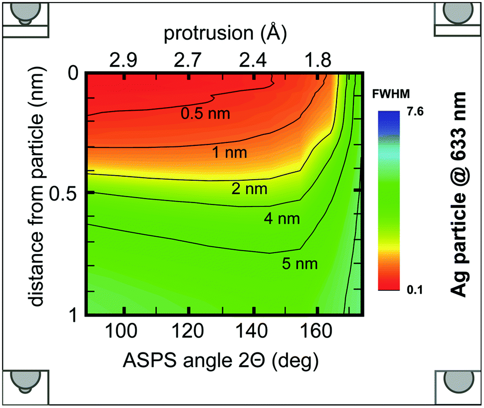 | ||
| Fig. 8 Color map with FWHM (nm) of the Raman enhancement (Eind/E0)4 with respect to the tip–sample distance and ASPS protrusion/angle. Calculated for a 20 nm Ag nanoparticle and excited at 633 nm (out-of-resonance). | ||
We consider the previous arguments regarding the calculated distances, and approximate the typical bond length involving metals (e.g. Ag–N) to about 3–3.5 Å between atom centers. With this value in hand, and based on the calculations presented in Fig. 7 and 8, a lateral resolution below 1 nm seems feasible, even under non-resonant conditions. While here conservative estimations are implemented, the exact resolution is strongly dependent on the particle–sample distance, the excitation energy (resonant or non-resonant), and the particle surface topography (substructure protrusion or angle).
It is noteworthy that here the distance between the particle and sample surface (Fig. 6–8) always refers to the distance between the outer shell from the metal atom and a point source as the sample. This is not to be confused with the core–core distance used in quantum mechanical calculations. While this difference is negligible in most cases, for distances below 1 nm it becomes important so as to avoid senseless definitions of a situation with a zero core–core distance that could still sustain a chemically attractive regime.34
Influence of tip oscillation on the Raman enhancement
As many TERS measurements are performed in an intermittent contact mode, the tip is most of the time quite far from the sample surface. We thus also calculated the enhancement for a typical TERS experiment in this dynamic mode. In such a situation, the tip will oscillate with a certain frequency and amplitude during the Raman measurement (Fig. 9). The detected signal is an averaged signal over all particle–molecule distances, d, during the acquisition time. To consider this, we have calculated the Raman enhancement factor and the respective FWHMs for a single harmonic tip oscillation, under non-resonant conditions. Here the field was calculated with respect to all particle–molecule distance configurations. Consequently the oscillation period was discretized in k segments, therefore the corresponding height of each segment (Zn) was calculated using: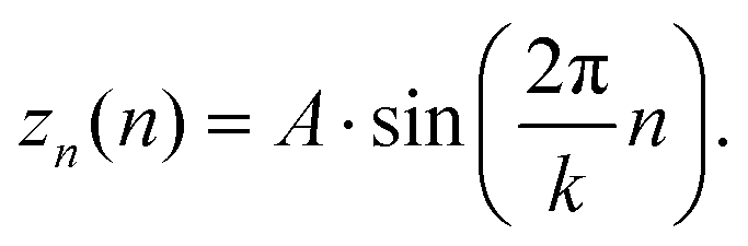 | (3) |
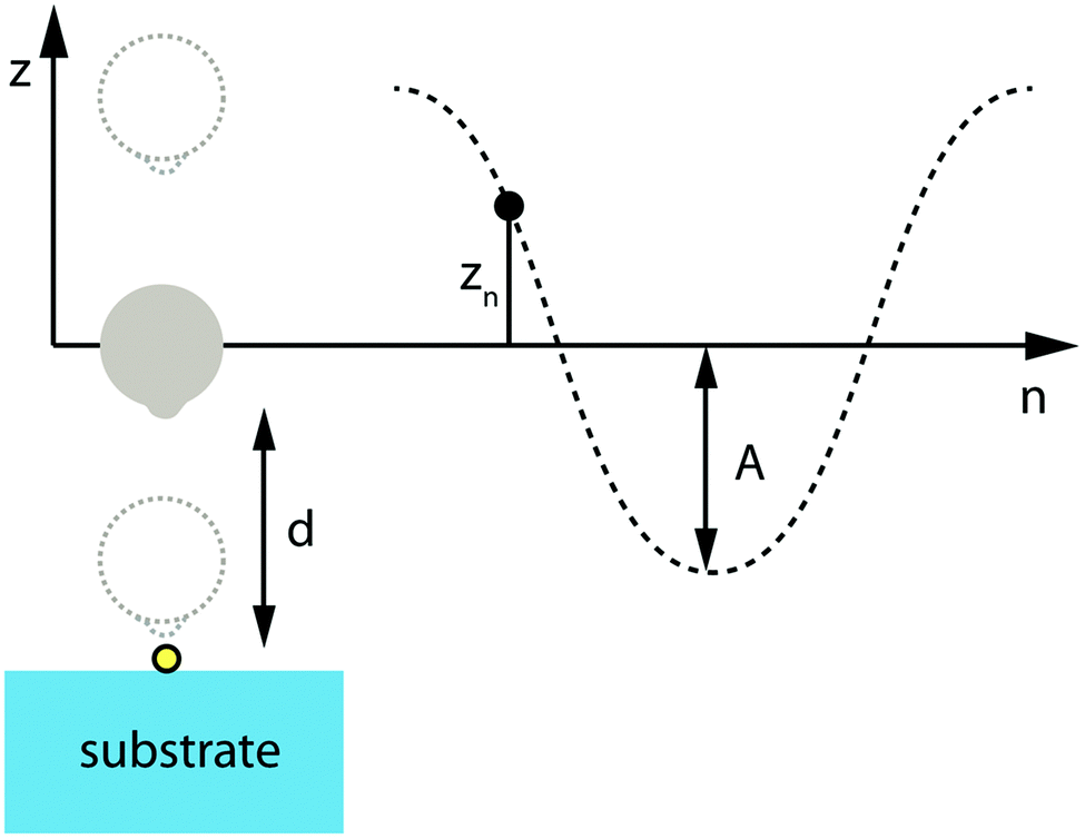 | ||
| Fig. 9 Schematic representation of the sinusoidal oscillation of a TERS probe (20 nm Ag nanoparticle + substructure) above a virtual molecule. | ||
A represents the tip-oscillation amplitude. Here a typical experimental value of ±5 nm was chosen.
For calculating the particle–molecule distance dependence on the segment, a summation with an offset value was used. The offset value is the displacement of the oscillation center with respect to the surface, i.e. here A/2+ the minimum tip–sample approach (here 0.2 nm closest surface distance) resulting in an offset of 5.2 nm.
| d(n) = offset + Zn(n) | (4) |
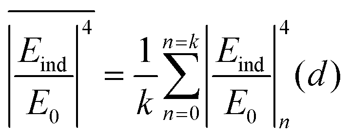
The maximum Raman enhancement factors and the corresponding FWHMs are plotted in Fig. 10 as a function of the tip–molecule distance, d, for a single half-period. The average Raman enhancement factor (black dotted line in Fig. 10) was calculated by the following formula, with the enhancing field (non-resonant case Ag tip) at the molecule position expressed as a function of d.
 | (5) |
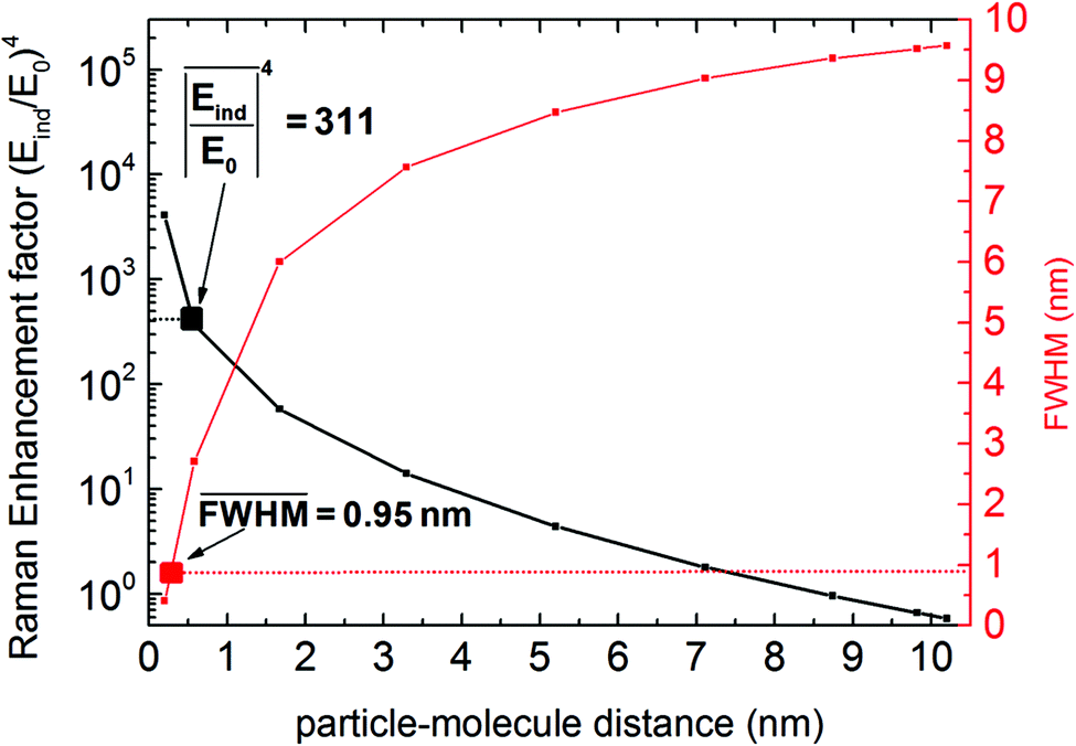 | ||
| Fig. 10 Distance dependence of the Raman enhancement factor (Eind/E0)4 and FWHM for an Ag nanoparticle (R = 10 nm) excited at 633 nm. Average Raman enhancement factor (black dotted line) and average FWHM (red dotted line) calculated for one sinusoidal oscillation with an amplitude of 10 nm and a minimum particle–molecule distance (d) of 0.2 nm. | ||
The average FWHM (red dotted line Fig. 10) can be similarly calculated by weighing all the possible FWHMs with the respective Raman enhancement factors. This way, the higher intensity contributions also dominate the FWHM.
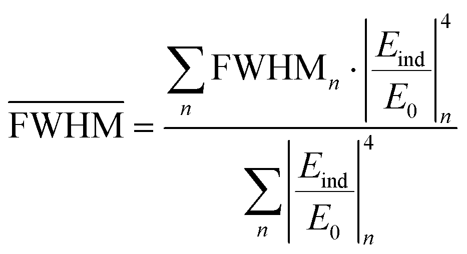 | (6) |
For the situation considered here, we calculated an average lateral resolution of 0.95 nm and an average Raman enhancement factor of 311 for the non-resonant case. This calculation enables a quantitative estimation of the average enhancement factor and of the lateral resolution (FWHM) for one periodical oscillation in TERS experiments (Fig. 10). While this average Raman enhancement strongly depends on the closest particle–molecule distance and on the exact resonance conditions of the nanoparticle, the conservatively (non-resonantly) computed values correlate well with previous experimental results.8,17
Conclusions
We have presented an extended classical FEM calculation that models near-field plasmonic probes with atomic scale substructures in order to provide a deeper understanding and theoretically relevant explanation for recent near-field experiments (e.g. enhancement and lateral resolution) that have led to the achievement of unexpectedly high lateral resolution. The proposed model system enables a straight forward approximation of realistic TERS probe surface topographies by the incorporation of atomic features onto spherical metallic particles. Systematic variations of the atomic-scale substructure angle and/or protrusion have revealed the dependencies of the field enhancement on these topographical features. Importantly, the axial field distribution caused by atomic features has been shown to be extremely localized, namely in the subnanometer regime.As expected, the actual field relies on several factors, such as the ASPS protrusion, excitation wavelength, the nature of the material forming the tip and the atomic-scale features, as well as additional geometric factors (e.g. MIM structures). Interestingly, the field enhancement and lateral resolution (FWHM) for non-resonantly excited nanoparticles are less dependent on the ASPS protrusion than in resonant cases. The most critical factor for both enhancement and lateral resolution is the tip–sample distance d. If the sample (e.g. a molecule) is more than 1 nm away from the particle surface, the atomic scale features have only a negligible effect on both aspects. However, at closer distances, these surface hotspots start to significantly contribute to the signal enhancement. Particularly under the non-resonant conditions the results suggest that even minute deviations of the base particle surface are sufficient to induce a further localization of the fields.
Furthermore, the influence of the tip oscillation on the Raman signal has been quantitatively investigated. As a consequence of the rapid field decay, the enhancement (and thus the lateral resolution) is dominated at close distances. The field contributions at large tip–sample distances can be almost neglected. For a typical TERS oscillation amplitude of ±5 nm a mean lateral resolution below 1 nm was determined even under non-resonant conditions. Clearly, values for real systems are strongly dependent on the closest distance between the metal surface and molecule, which is set here arbitrarily to 2 Å. On the other hand, TERS is usually performed under resonant excitation conditions. This would yield a much higher enhancement and resolution. Hence, we are confident that the quantitative estimations provided here are quite conservative, within the limits of the model.
Important aspects of the field variations at least on a molecular scale are the consequences on the Raman selection rules. This significantly impacts the interpretation of experimental results, as recent studies have demonstrated. The strong inhomogeneity of the local fields highlighted here calls for more accurate first principles calculations of the Raman spectra, where the strong inhomogeneous nature of the field at the atomic scale is taken into account.
In comparison to quantum mechanical models such as TDDFT that calculate the optical response of nanoparticles with realistic shapes, our classical model system can be implemented effortlessly and allows faster computations. Consequently, different shapes of the base particle and the sub-structure can be tested for specific experimental situations. While this method cannot replace quantum mechanical calculations, we have demonstrated its usefulness for accessible quantitative predictions of spatial resolution in near-field methods. Overall, we believe that it paves the way to a better understanding and a more accurate interpretation of the surprisingly high spatial resolution that can be reached in typical TERS experiments.
Acknowledgements
We gratefully acknowledge financial support from the Thuringian State Government within its ProExcellence initiative (APC2020). S. T. would like to thank Tomas Neuman for helpful discussions and COST (COST-STSM-MP1302-21198) for financial support. J. A. acknowledges the hospitality of the Abbe Center in Jena, and financial support of project FIS2013-41184-P of the Spanish MINECO, and project IT756-13 of the Department of Education and Culture of the Government of the Basque Country.References
- M. Moskovits, Rev. Mod. Phys., 1985, 57, 783–826 CrossRef CAS.
- P. Bharadwaj and L. Novotny, Opt. Express, 2007, 15, 14266 CrossRef CAS PubMed.
- U. Kreibig and M. Vollmer, Optical Properties of Metal Clusters, Springer, Berlin, Heidelberg, 1995, vol. 25 Search PubMed.
- M. Cardona and G. Güntherodt, Light Scattering in Solids IV, Springer, Berlin, Heidelberg, 1984 Search PubMed.
- S. A. Maier, Plasmonics: Fundamentals and Applications, Springer Science & Business Media, 2007, p. 224 Search PubMed.
- F. Zenhausern, M. P. O'Boyle and H. K. Wickramasinghe, Appl. Phys. Lett., 1994, 65, 1623 CrossRef CAS.
- R. M. Stöckle, Y. D. Suh, V. Deckert and R. Zenobi, Chem. Phys. Lett., 2000, 318, 131–136 CrossRef.
- B. Pettinger, P. Schambach, C. J. Villagómez and N. Scott, Annu. Rev. Phys. Chem., 2012, 63, 379–399 CrossRef CAS PubMed.
- H. Xu, E. J. Bjerneld, M. Käll and L. Börjesson, Phys. Rev. Lett., 1999, 83, 4357–4360 CrossRef CAS.
- H. Xu, J. Aizpurua, M. Käll and P. Apell, Phys. Rev. E, 2000, 62, 4318–4324 CrossRef CAS.
- D. K. Gramotnev and S. I. Bozhevolnyi, Nat. Photonics, 2010, 4, 83–91 CrossRef CAS.
- K. J. Savage, M. M. Hawkeye, R. Esteban, A. G. Borisov, J. Aizpurua and J. J. Baumberg, Nature, 2012, 491, 574–577 CrossRef CAS PubMed.
- F. Benz, M. K. Schmidt, A. Dreismann, R. Chikkaraddy, Y. Zhang, A. Demetriadou, C. Carnegie, H. Ohadi, B. de Nijs, R. Esteban, J. Aizpurua and J. J. Baumberg, Science, 2016, 354, 726–729 CrossRef CAS PubMed.
- J. Li, J. Mu, B. Wang, W. Ding, J. Liu, H. Guo, W. Li, C. Gu and Z.-Y. Li, Laser Photonics Rev., 2014, 8, 602–609 CrossRef CAS.
- T. L. Vasconcelos, B. S. Archanjo, B. Fragneaud, B. S. Oliveira, J. Riikonen, C. Li, D. S. Ribeiro, C. Rabelo, W. N. Rodrigues, A. Jorio, C. A. Achete and L. G. Cançado, ACS Nano, 2015, 9, 6297–6304 CrossRef CAS PubMed.
- S. Berweger, J. M. Atkin, R. L. Olmon and M. B. Raschke, J. Phys. Chem. Lett., 2012, 3, 945–952 CrossRef CAS PubMed.
- R. Zhang, Y. Zhang, Z. C. Dong, S. Jiang, C. Zhang, L. G. Chen, L. Zhang, Y. Liao, J. Aizpurua, Y. Luo, J. L. Yang and J. G. Hou, Nature, 2013, 498, 82–86 CrossRef CAS PubMed.
- S. Jiang, Y. Zhang, R. Zhang, C. Hu, M. Liao, Y. Luo, J. Yang, Z. Dong and J. G. Hou, Nat. Nanotechnol., 2015, 10, 865–869 CrossRef CAS PubMed.
- F. Zenhausern, Y. Martin and H. K. Wickramasinghe, Science, 1995, 269, 1083–1085 CrossRef CAS PubMed.
- W. Zhang, X. Cui, B.-S. Yeo, T. Schmid, C. Hafner and R. Zenobi, Nano Lett., 2007, 7, 1401–1405 CrossRef CAS PubMed.
- N. Chiang, X. Chen, G. Goubert, D. V. Chulhai, X. Chen, E. A. Pozzi, N. Jiang, M. C. Hersam, T. Seideman, L. Jensen and R. P. Van Duyne, Nano Lett., 2016 DOI:10.1021/acs.nanolett.6b03958.
- F. J. García-Vidal and J. B. Pendry, Phys. Rev. Lett., 1996, 77, 1163–1166 CrossRef PubMed.
- I. Notingher and A. Elfick, J. Phys. Chem. B, 2005, 109, 15699–15706 CrossRef CAS PubMed.
- J. A. Scholl, A. García-Etxarri, A. L. Koh and J. A. Dionne, Nano Lett., 2013, 13, 564–569 CrossRef CAS PubMed.
- Y. Liu and Y. Sun, Nanoscale, 2015, 7, 13687–13693 RSC.
- A. M. Kern and O. J. F. Martin, Nano Lett., 2011, 11, 482–487 CrossRef CAS PubMed.
- A. Trügler, J.-C. Tinguely, J. R. Krenn, A. Hohenau and U. Hohenester, Phys. Rev. B, 2011, 83, 081412 CrossRef.
- P. Dawson, J. A. Duenas, M. G. Boyle, M. D. Doherty, S. E. J. Bell, A. M. Kern, O. J. F. Martin, A.-S. Teh, K. B. K. Teo and W. I. Milne, Nano Lett., 2011, 11, 365–371 CrossRef CAS PubMed.
- M. Barbry, P. Koval, F. Marchesin, R. Esteban, A. G. Borisov, J. Aizpurua and D. Sánchez-Portal, Nano Lett., 2015, 15, 3410–3419 CrossRef CAS PubMed.
- P. Zhang, J. Feist, A. Rubio, P. García-González and F. J. García-Vidal, Phys. Rev. B: Condens. Matter, 2014, 90, 161407 CrossRef.
- A. Varas, P. García-González, F. J. García-Vidal and A. Rubio, J. Phys. Chem. Lett., 2015, 6, 1891–1898 CrossRef CAS PubMed.
- M. J. McClain, A. E. Schlather, E. Ringe, N. S. King, L. Liu, A. Manjavacas, M. W. Knight, I. Kumar, K. H. Whitmire, H. O. Everitt, P. Nordlander and N. J. Halas, Nano Lett., 2015, 15, 2751–2755 CrossRef CAS PubMed.
- J. Nelayah, M. Kociak, O. Stéphan, F. J. García de Abajo, M. Tencé, L. Henrard, D. Taverna, I. Pastoriza-Santos, L. M. Liz-Marzán and C. Colliex, Nat. Phys., 2007, 3, 348–353 CrossRef CAS.
- F. Latorre, S. Kupfer, T. Bocklitz, D. Kinzel, S. Trautmann, S. Gräfe and V. Deckert, Nanoscale, 2016, 8, 10229–10239 RSC.
- T. V. Teperik, P. Nordlander, J. Aizpurua and A. G. Borisov, Opt. Express, 2013, 21, 27306 CrossRef PubMed.
- C. Blum, L. Opilik, J. M. Atkin, K. Braun, S. B. Kämmer, V. Kravtsov, N. Kumar, S. Lemeshko, J.-F. Li, K. Luszcz, T. Maleki, A. J. Meixner, S. Minne, M. B. Raschke, B. Ren, J. Rogalski, D. Roy, B. Stephanidis, X. Wang, D. Zhang, J.-H. Zhong and R. Zenobi, J. Raman Spectrosc., 2014, 45, 22–31 CrossRef CAS.
- T. Kalkbrenner, M. Ramstein, J. Mlynek and V. Sandoghdar, J. Microsc., 2001, 202, 72–76 CrossRef CAS PubMed.
- D. Germund and Å. Björck, Numerische Methoden, Oldenbourg München, 1972 Search PubMed.
- L. C. Davis, Phys. Rev. B: Solid State, 1976, 14, 5523–5525 CrossRef.
- Y. Luo, J. B. Pendry and A. Aubry, Nano Lett., 2010, 10, 4186–4191 CrossRef CAS PubMed.
- E. Clementi, J. Chem. Phys., 1967, 47, 1300 CrossRef CAS.
- P. B. Johnson and R. W. Christy, Phys. Rev. B, 1972, 6, 4370–4379 CrossRef CAS.
- A. Taguchi, J. Yu, P. Verma and S. Kawata, Nanoscale, 2015, 7, 17424–17433 RSC.
Footnote |
| † Electronic supplementary information (ESI) available. See DOI: 10.1039/c6nr07560f |
| This journal is © The Royal Society of Chemistry 2017 |